d3035167c17b0aa0c9454786a6bfdc2a.ppt
- Количество слайдов: 62
 X-ray Diffraction (XRD) • What is X-ray Diffraction Properties and generation of X-ray • Bragg’s Law • Basics of Crystallography • XRD Pattern • Powder Diffraction • Applications of XRD http: //www. matter. org. uk/diffraction/x-ray/default. htm
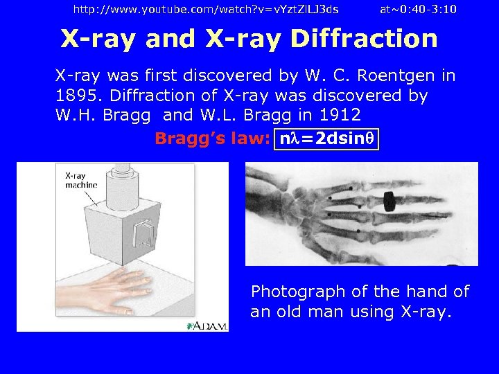 http: //www. youtube. com/watch? v=v. Yzt. Zl. LJ 3 ds at~0: 40 -3: 10 X-ray and X-ray Diffraction X-ray was first discovered by W. C. Roentgen in 1895. Diffraction of X-ray was discovered by W. H. Bragg and W. L. Bragg in 1912 Bragg’s law: n =2 dsin Photograph of the hand of an old man using X-ray.
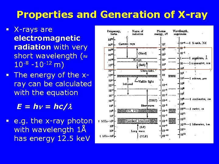 Properties and Generation of X-ray § X-rays are electromagnetic radiation with very short wavelength ( 10 -8 -10 -12 m) § The energy of the xray can be calculated with the equation E = hc/ § e. g. the x-ray photon with wavelength 1Å has energy 12. 5 ke. V
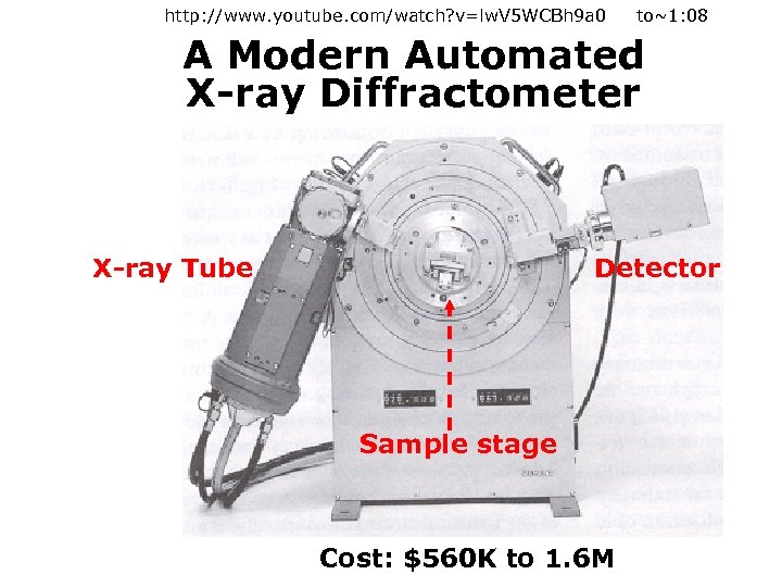 http: //www. youtube. com/watch? v=lw. V 5 WCBh 9 a 0 to~1: 08 A Modern Automated X-ray Diffractometer X-ray Tube Detector Sample stage Cost: $560 K to 1. 6 M
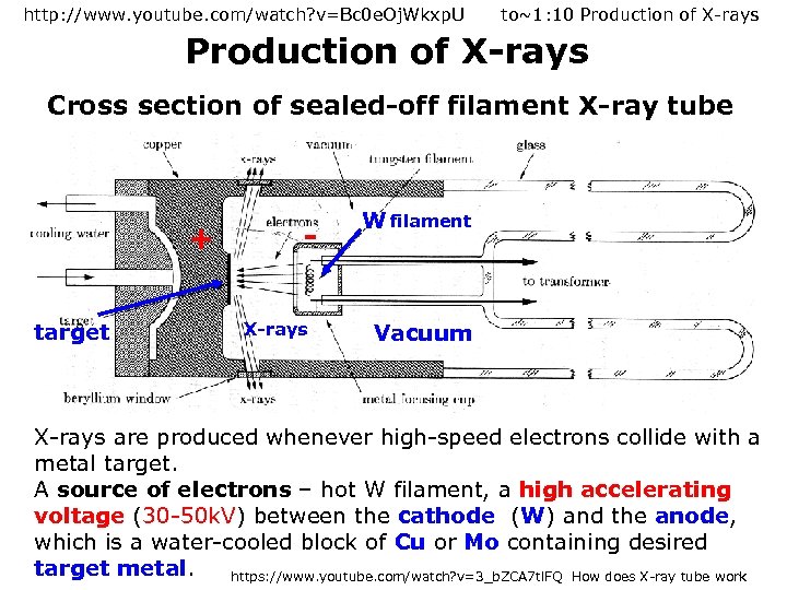 http: //www. youtube. com/watch? v=Bc 0 e. Oj. Wkxp. U to~1: 10 Production of X-rays Cross section of sealed-off filament X-ray tube + target X-rays W filament Vacuum X-rays are produced whenever high-speed electrons collide with a metal target. A source of electrons – hot W filament, a high accelerating voltage (30 -50 k. V) between the cathode (W) and the anode, which is a water-cooled block of Cu or Mo containing desired target metal. https: //www. youtube. com/watch? v=3_b. ZCA 7 tl. FQ How does X-ray tube work
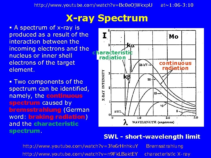 http: //www. youtube. com/watch? v=Bc 0 e. Oj. Wkxp. U at~1: 06 -3: 10 X-ray Spectrum § A spectrum of x-ray is produced as a result of the I Mo interaction between the k incoming electrons and the characteristic nucleus or inner shell radiation electrons of the target continuous radiation element. k § Two components of the spectrum can be identified, namely, the continuous spectrum caused by bremsstrahlung (German word: braking radiation) and the characteristic spectrum. SWL - short-wavelength limit http: //www. youtube. com/watch? v=3 fe 6 r. Hnhku. Y http: //www. youtube. com/watch? v=n 9 Fk. LBakt. EY Bremsstrahlung characteristic X-ray
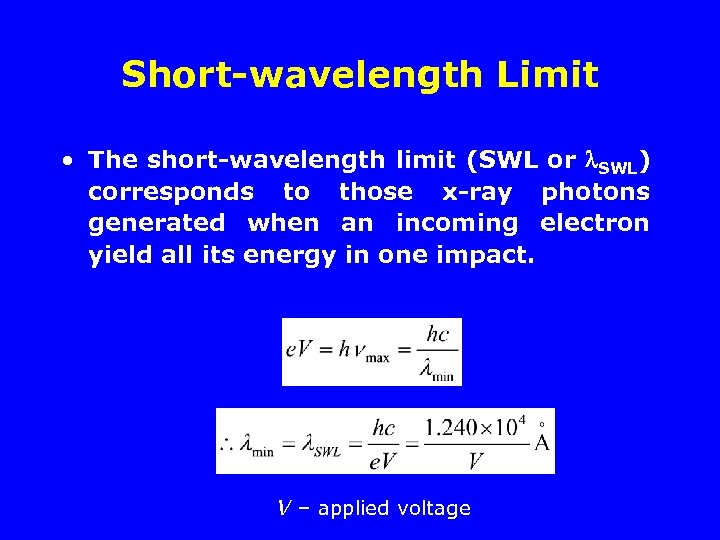 Short-wavelength Limit • The short-wavelength limit (SWL or SWL) corresponds to those x-ray photons generated when an incoming electron yield all its energy in one impact. V – applied voltage
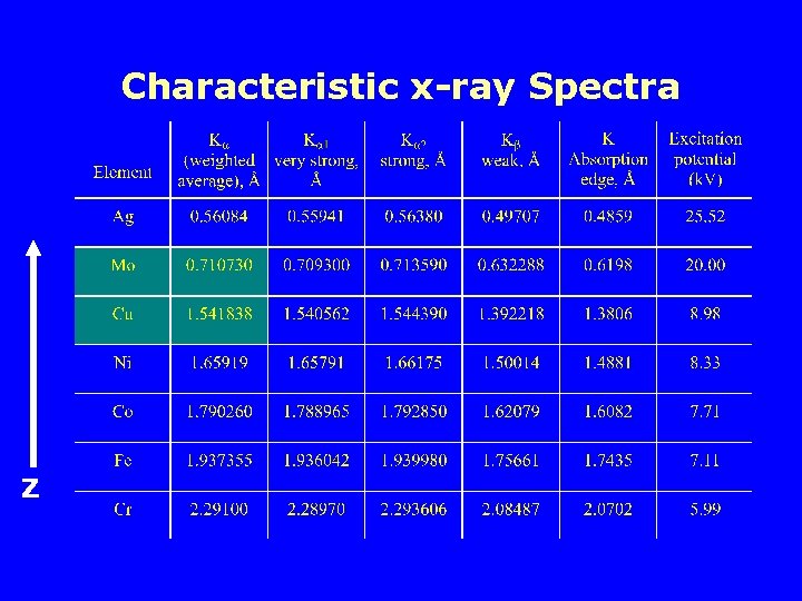
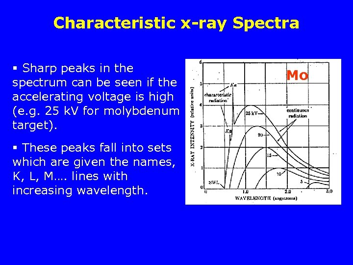 Characteristic x-ray Spectra § Sharp peaks in the spectrum can be seen if the accelerating voltage is high (e. g. 25 k. V for molybdenum target). § These peaks fall into sets which are given the names, K, L, M…. lines with increasing wavelength. Mo
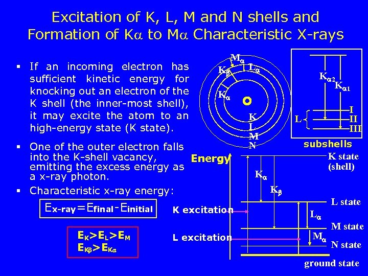 Excitation of K, L, M and N shells and Formation of K to M Characteristic X-rays § If an incoming electron has sufficient kinetic energy for knocking out an electron of the K shell (the inner-most shell), it may excite the atom to an high-energy state (K state). K M EK>EL>EM EK >EK 3/17/2018 K 2 K 1 K § One of the outer electron falls into the K-shell vacancy, Energy emitting the excess energy as a x-ray photon. § Characteristic x-ray energy: Ex-ray=Efinal-Einitial L K excitation L excitation K L M N I II III L subshells K state (shell) K K L state L M M state N state ground state
 Characteristic x-ray Spectra Z
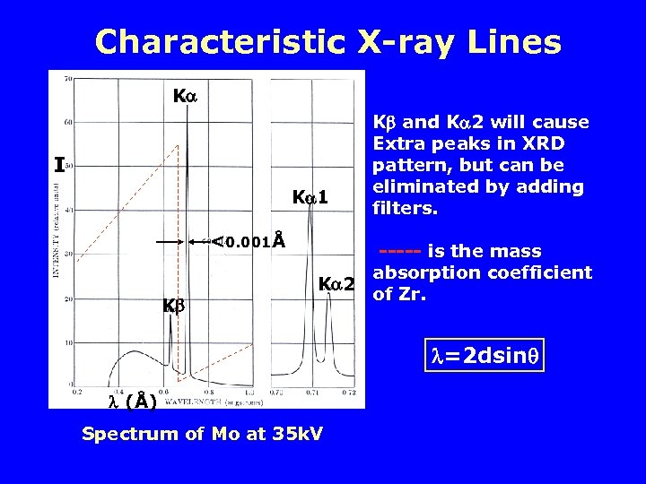 Characteristic X-ray Lines K I K 1 <0. 001Å K K and K 2 will cause Extra peaks in XRD pattern, but can be eliminated by adding filters. ----- is the mass absorption coefficient K 2 of Zr. =2 dsin (Å) Spectrum of Mo at 35 k. V
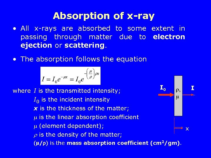 Absorption of x-ray • All x-rays are absorbed to some extent in passing through matter due to electron ejection or scattering. • The absorption follows the equation where I is the transmitted intensity; I 0 is the incident intensity x is the thickness of the matter; is the linear absorption coefficient (element dependent); is the density of the matter; I 0 I I , ( / ) is the mass absorption coefficient (cm 2/gm). x x
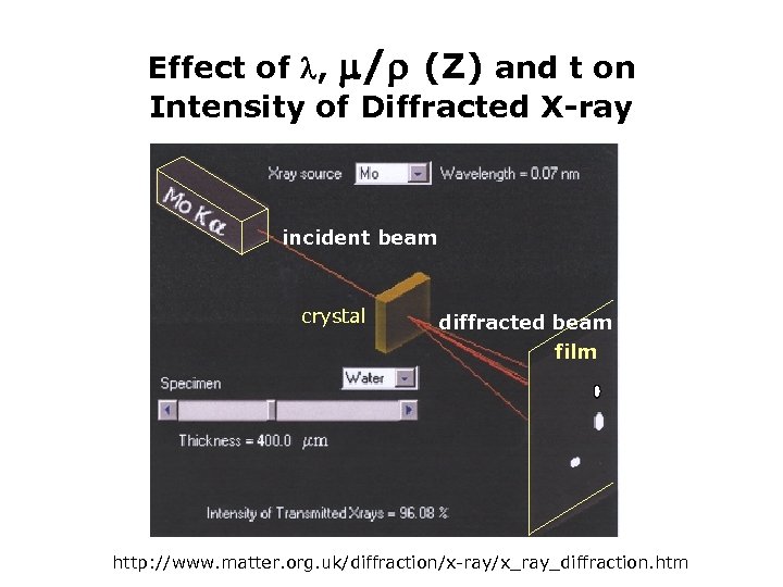 Effect of , / (Z) and t on Intensity of Diffracted X-ray incident beam crystal diffracted beam film http: //www. matter. org. uk/diffraction/x-ray/x_ray_diffraction. htm
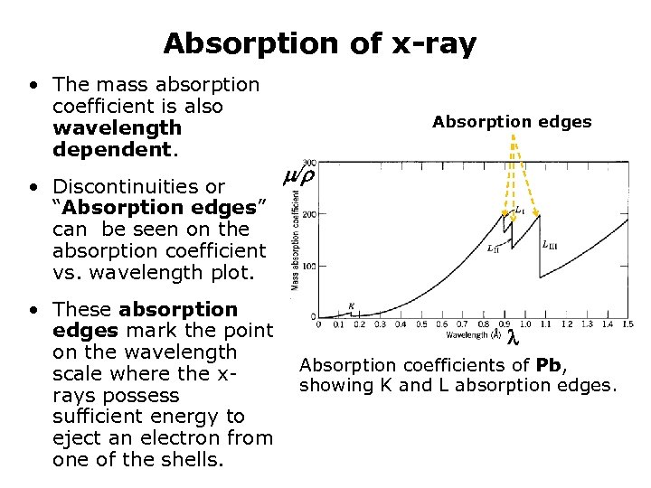 Absorption of x-ray • The mass absorption coefficient is also wavelength dependent. • Discontinuities or “Absorption edges” can be seen on the absorption coefficient vs. wavelength plot. • These absorption edges mark the point on the wavelength scale where the xrays possess sufficient energy to eject an electron from one of the shells. Absorption edges / Absorption coefficients of Pb, showing K and L absorption edges.
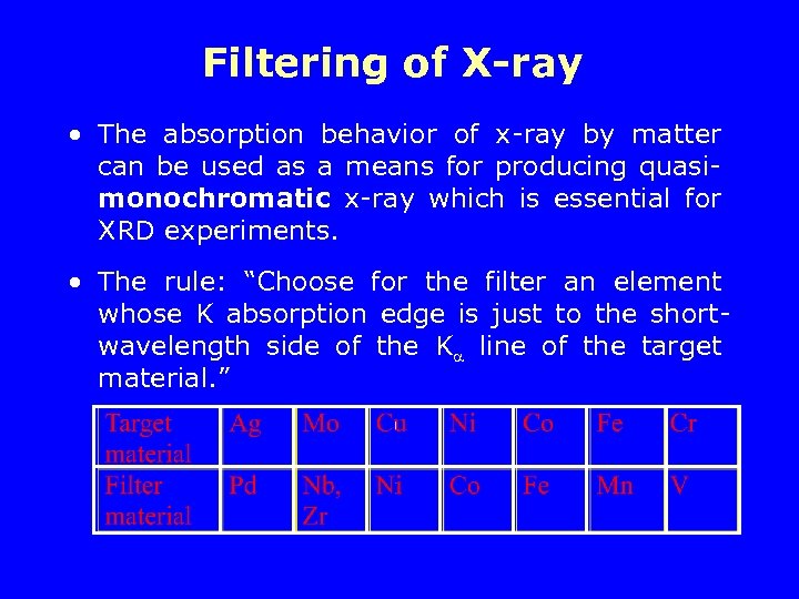 Filtering of X-ray • The absorption behavior of x-ray by matter can be used as a means for producing quasimonochromatic x-ray which is essential for XRD experiments. • The rule: “Choose for the filter an element whose K absorption edge is just to the shortwavelength side of the K line of the target material. ”
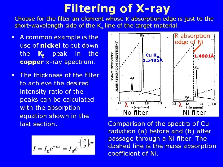 Filtering of X-ray Choose for the filter an element whose K absorption edge is just to the short-wavelength side of the K line of the target material. § A common example is the use of nickel to cut down the K peak in the copper x-ray spectrum. § The thickness of the filter to achieve the desired intensity ratio of the peaks can be calculated with the absorption equation shown in the last section. K absorption edge of Ni Cu K 1. 5405Å No filter 1. 4881Å Ni filter Comparison of the spectra of Cu radiation (a) before and (b) after passage through a Ni filter. The dashed line is the mass absorption coefficient of Ni.
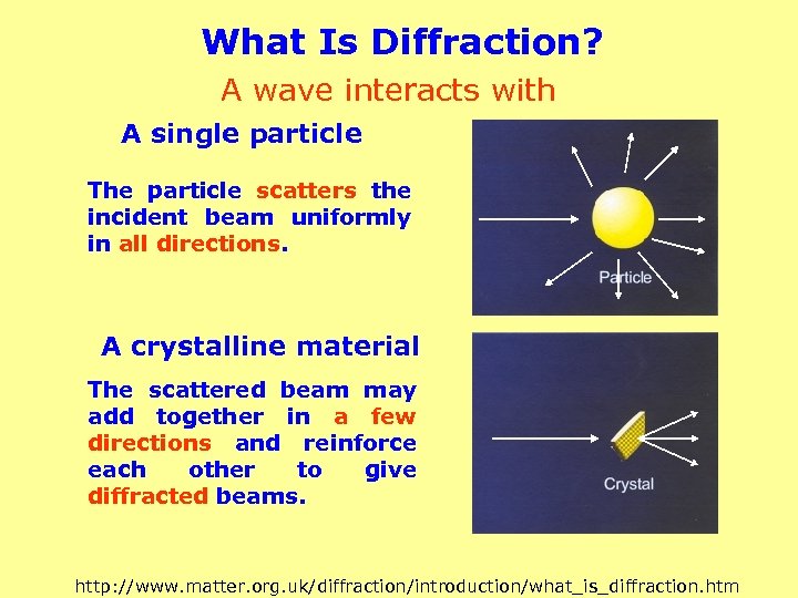 What Is Diffraction? A wave interacts with A single particle The particle scatters the incident beam uniformly in all directions. A crystalline material The scattered beam may add together in a few directions and reinforce each other to give diffracted beams. http: //www. matter. org. uk/diffraction/introduction/what_is_diffraction. htm
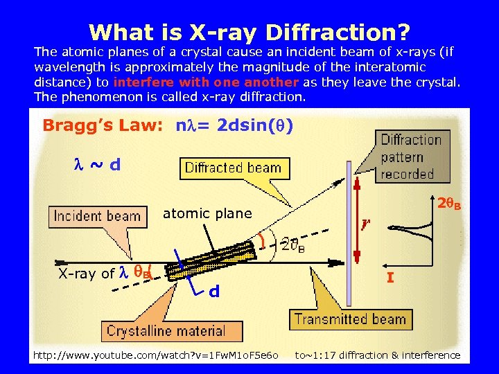 What is X-ray Diffraction? The atomic planes of a crystal cause an incident beam of x-rays (if wavelength is approximately the magnitude of the interatomic distance) to interfere with one another as they leave the crystal. The phenomenon is called x-ray diffraction. Bragg’s Law: n = 2 dsin( ) ~d 2 B atomic plane X-ray of B d http: //www. youtube. com/watch? v=1 Fw. M 1 o. F 5 e 6 o I to~1: 17 diffraction & interference
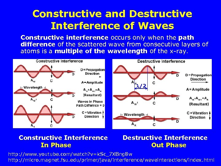 Constructive and Destructive Interference of Waves Constructive interference occurs only when the path difference of the scattered wave from consecutive layers of atoms is a multiple of the wavelength of the x-ray. /2 Constructive Interference In Phase Destructive Interference Out Phase http: //www. youtube. com/watch? v=k. Sc_7 XBng 8 w http: //micro. magnet. fsu. edu/primer/java/interference/waveinteractions/index. html
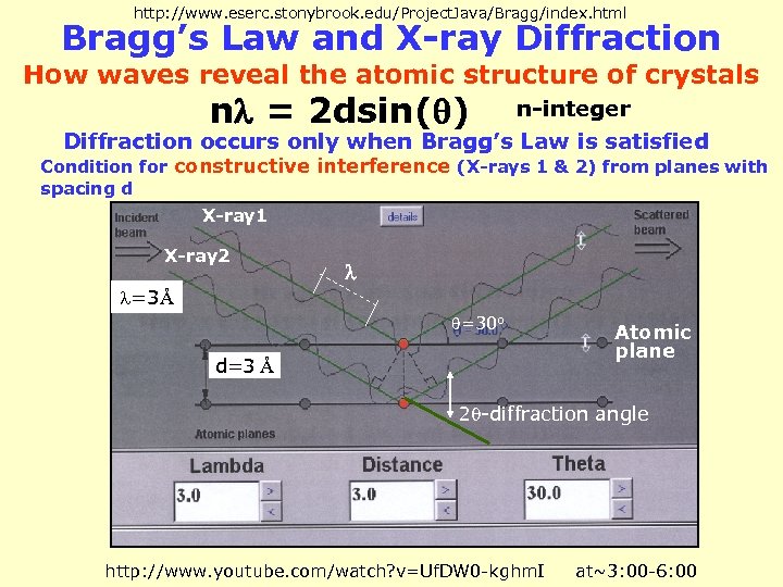 http: //www. eserc. stonybrook. edu/Project. Java/Bragg/index. html Bragg’s Law and X-ray Diffraction How waves reveal the atomic structure of crystals n = 2 dsin( ) n-integer Diffraction occurs only when Bragg’s Law is satisfied Condition for constructive interference (X-rays 1 & 2) from planes with spacing d X-ray 1 X-ray 2 =3Å =30 o d=3 Å Atomic plane 2 -diffraction angle http: //www. youtube. com/watch? v=Uf. DW 0 -kghm. I at~3: 00 -6: 00
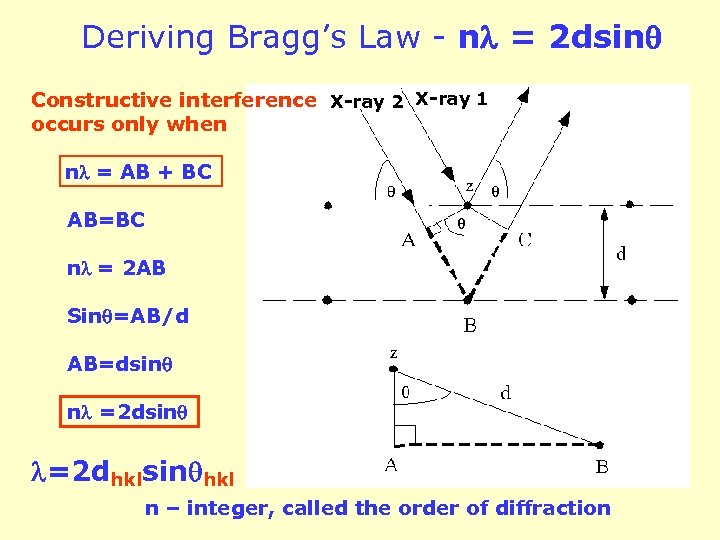 Deriving Bragg’s Law - n = 2 dsin Constructive interference X-ray 2 X-ray 1 occurs only when n = AB + BC AB=BC n = 2 AB Sin =AB/d AB=dsin n =2 dsin =2 dhklsin hkl n – integer, called the order of diffraction
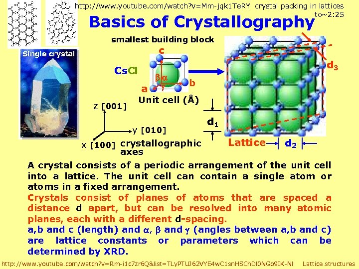 http: //www. youtube. com/watch? v=Mm-jqk 1 Te. RY crystal packing in lattices to~2: 25 Basics of Crystallography smallest building block c Single crystal Cs. Cl z [001] d 3 b a Unit cell (Å) d 1 y [010] Lattice d 2 x [100] crystallographic axes A crystal consists of a periodic arrangement of the unit cell into a lattice. The unit cell can contain a single atom or atoms in a fixed arrangement. Crystals consist of planes of atoms that are spaced a distance d apart, but can be resolved into many atomic planes, each with a different d-spacing. a, b and c (length) and , and (angles between a, b and c) are lattice constants or parameters which can be determined by XRD. http: //www. youtube. com/watch? v=Rm-i 1 c 7 zr 6 Q&list=TLy. PTUJ 62 VYE 4 w. C 1 sn. HSCh. Dl 0 NGo 9 IK-Nl Lattice structures
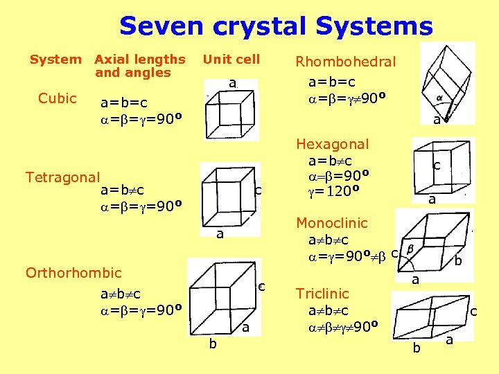 Seven crystal Systems System Axial lengths and angles Cubic Tetragonal Unit cell a a=b=c = = =90 o Rhombohedral a=b=c = = 90 o a a=b c = = =90 o c c b c a Monoclinic a b c = =90 o c a Orthorhombic a b c = = =90 o Hexagonal a=b c = =90 o =120 o a Triclinic a b c 90 o b a c b a
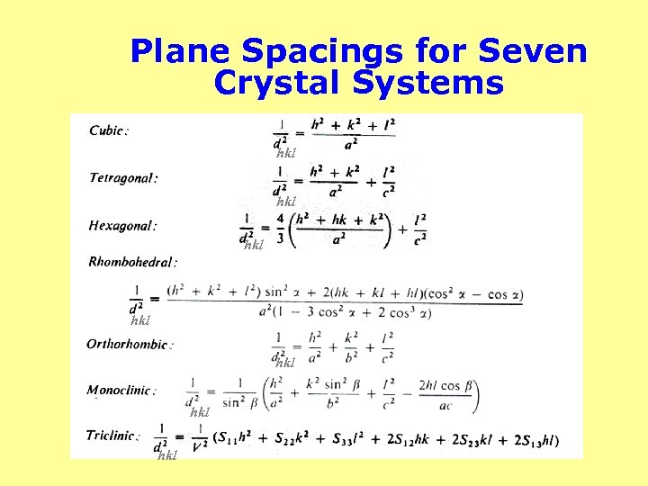 Plane Spacings for Seven Crystal Systems hkl 1 hkl hkl hkl
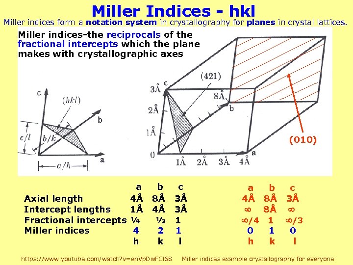 Miller Indices - hkl Miller indices form a notation system in crystallography for planes in crystal lattices. Miller indices-the reciprocals of the fractional intercepts which the plane makes with crystallographic axes (010) a Axial length 4Å Intercept lengths 1Å Fractional intercepts ¼ Miller indices 4 h b c 8Å 3Å 4Å 3Å ½ 1 2 1 k l https: //www. youtube. com/watch? v=en. Vp. Dw. FCl 68 a b 4Å 8Å /4 1 0 1 h k c 3Å /3 0 l Miller indices example crystallography for everyone
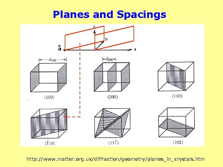 Planes and Spacings a http: //www. matter. org. uk/diffraction/geometry/planes_in_crystals. htm
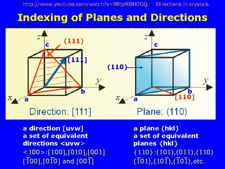 http: //www. youtube. com/watch? v=9 Rjp 9 i 0 H 7 GQ Directions in crystals Indexing of Planes and Directions c (111) [111] b c (110) b [110] a a a direction [uvw] a set of equivalent directions
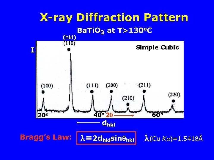 X-ray Diffraction Pattern (hkl) Ba. Ti. O 3 at T>130 o. C Simple Cubic I 20 o Bragg’s Law: 40 o 2 dhkl =2 dhklsin hkl 60 o (Cu K )=1. 5418Å
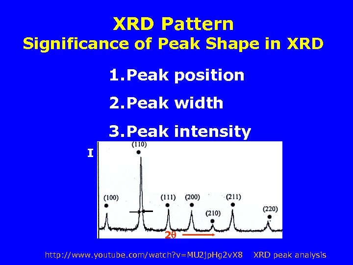 XRD Pattern Significance of Peak Shape in XRD 1. Peak position 2. Peak width 3. Peak intensity I 2 http: //www. youtube. com/watch? v=MU 2 jp. Hg 2 v. X 8 XRD peak analysis
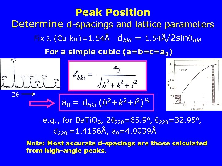 Peak Position Determine d-spacings and lattice parameters Fix (Cu k )=1. 54Å dhkl = 1. 54Å/2 sin hkl For a simple cubic (a=b=c=a 0) 2 a 0 = dhkl (h 2+k 2+l 2)½ e. g. , for Ba. Ti. O 3, 2 220=65. 9 o, 220=32. 95 o, d 220 =1. 4156Å, a 0=4. 0039Å Note: Most accurate d-spacings are those calculated from high-angle peaks.
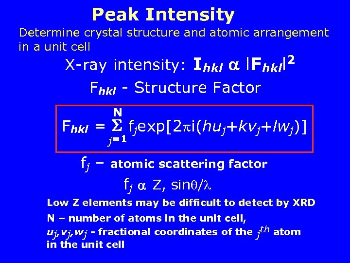 Peak Intensity Determine crystal structure and atomic arrangement in a unit cell X-ray intensity: Ihkl l. Fhkll 2 Fhkl - Structure Factor N Fhkl = fjexp[2 i(huj+kvj+lwj)] j=1 fj – atomic scattering factor fj Z, sin / Low Z elements may be difficult to detect by XRD N – number of atoms in the unit cell, uj, vj, wj - fractional coordinates of the jth atom in the unit cell
![Cubic Structures a=b=c=a Simple Cubic Body-centered Cubic Face-centered Cubic [001] BCC FCC z axis Cubic Structures a=b=c=a Simple Cubic Body-centered Cubic Face-centered Cubic [001] BCC FCC z axis](https://present5.com/presentation/d3035167c17b0aa0c9454786a6bfdc2a/image-32.jpg) Cubic Structures a=b=c=a Simple Cubic Body-centered Cubic Face-centered Cubic [001] BCC FCC z axis a a [100] x [010] y a 1 atom 2 atoms 8 x 1/8 =1 Location: 0, 0, 0 8 x 1/8 + 1 = 2 8 x 1/8 + 6 x 1/2 = 4 0, 0, 0, ½, ½, ½, 8 unit cells 4 atoms 0, 0, 0, ½, ½, 0, ½, ½, - corner atom, shared with 8 unit cells - atom at face-center, shared with 2 unit cells
Cubic Structures a=b=c=a Simple Cubic Body-centered Cubic Face-centered Cubic [001] BCC FCC z axis a a [100] x [010] y a 1 atom 2 atoms 8 x 1/8 =1 Location: 0, 0, 0 8 x 1/8 + 1 = 2 8 x 1/8 + 6 x 1/2 = 4 0, 0, 0, ½, ½, ½, 8 unit cells 4 atoms 0, 0, 0, ½, ½, 0, ½, ½, - corner atom, shared with 8 unit cells - atom at face-center, shared with 2 unit cells
![Structures of Some Common Metals [001] axis = 2 dhklsin hkl (001) plane d Structures of Some Common Metals [001] axis = 2 dhklsin hkl (001) plane d](https://present5.com/presentation/d3035167c17b0aa0c9454786a6bfdc2a/image-33.jpg) Structures of Some Common Metals [001] axis = 2 dhklsin hkl (001) plane d 010 Mo a d 001 (002) d 002 = ½ a [100] a a [010] BCC FCC h, k, l – integers, Miller indices, (hkl) planes (001) plane intercept [001] axis with a length of a, l = 1 (002) plane intercept [001] axis with a length of ½ a, l = 2 (010) plane intercept [010] axis with a length of a, k = 1, etc. Cu (010) plane [010] axis
Structures of Some Common Metals [001] axis = 2 dhklsin hkl (001) plane d 010 Mo a d 001 (002) d 002 = ½ a [100] a a [010] BCC FCC h, k, l – integers, Miller indices, (hkl) planes (001) plane intercept [001] axis with a length of a, l = 1 (002) plane intercept [001] axis with a length of ½ a, l = 2 (010) plane intercept [010] axis with a length of a, k = 1, etc. Cu (010) plane [010] axis
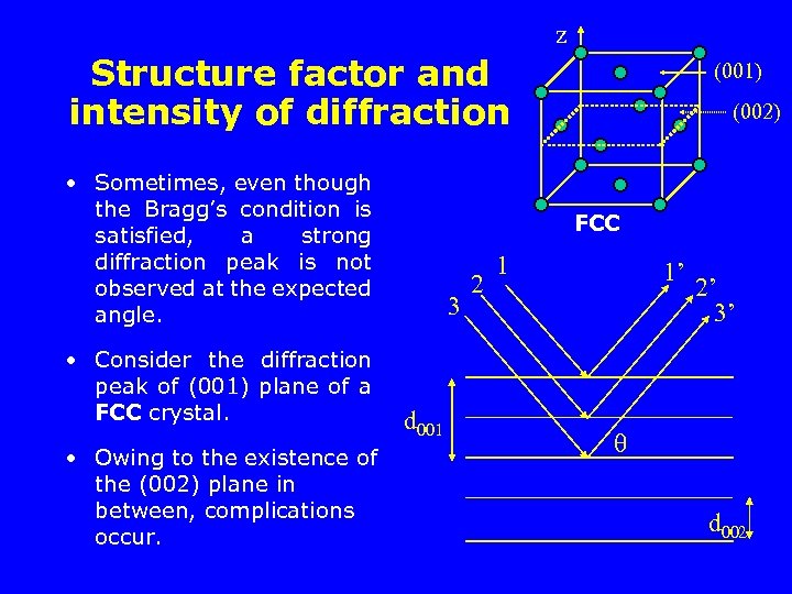 z Structure factor and intensity of diffraction • Sometimes, even though the Bragg’s condition is satisfied, a strong diffraction peak is not observed at the expected angle. • Consider the diffraction peak of (001) plane of a FCC crystal. • Owing to the existence of the (002) plane in between, complications occur. (001) (002) FCC 3 d 001 2 1 1’ 2’ 3’ d 002
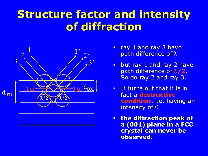 Structure factor and intensity of diffraction 3 d 001 2 1 1’ /4 /2 2’ 3’ d 002 § ray 1 and ray 3 have path difference of § but ray 1 and ray 2 have path difference of /2. So do ray 2 and ray 3. § It turns out that it is in fact a destructive condition, i. e. having an intensity of 0. § the diffraction peak of a (001) plane in a FCC crystal can never be observed.
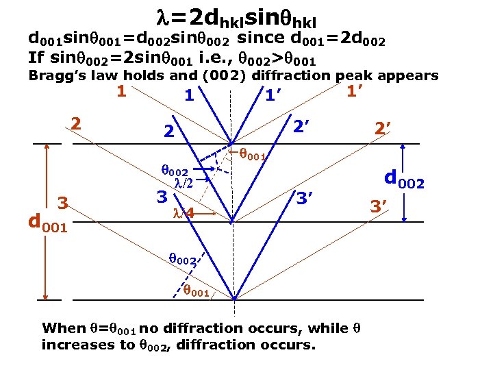 http: //emalwww. engin. umich. edu/education_materials/microscopy. html =2 dhklsin hkl d 001 sin 001=d 002 sin 002 since d 001=2 d 002 If sin 002=2 sin 001 i. e. , 002> 001 Bragg’s law holds and (002) diffraction peak appears 1 2’ 2 002 /2 3 d 001 3 1’ 1’ /4 2’ 001 3’ 002 001 When = 001 no diffraction occurs, while increases to 002, diffraction occurs. d 002 3’
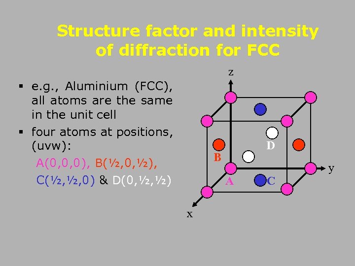 Structure factor and intensity of diffraction for FCC z § e. g. , Aluminium (FCC), all atoms are the same in the unit cell § four atoms at positions, (uvw): A(0, 0, 0), B(½, 0, ½), C(½, ½, 0) & D(0, ½, ½) D B y A x C
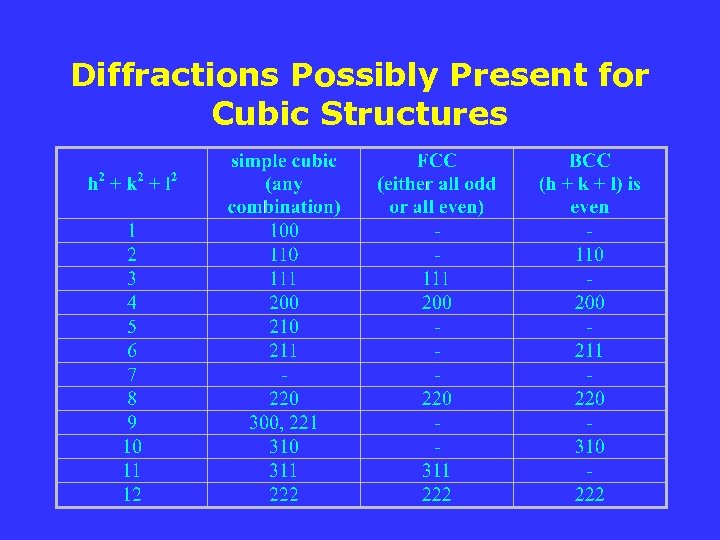
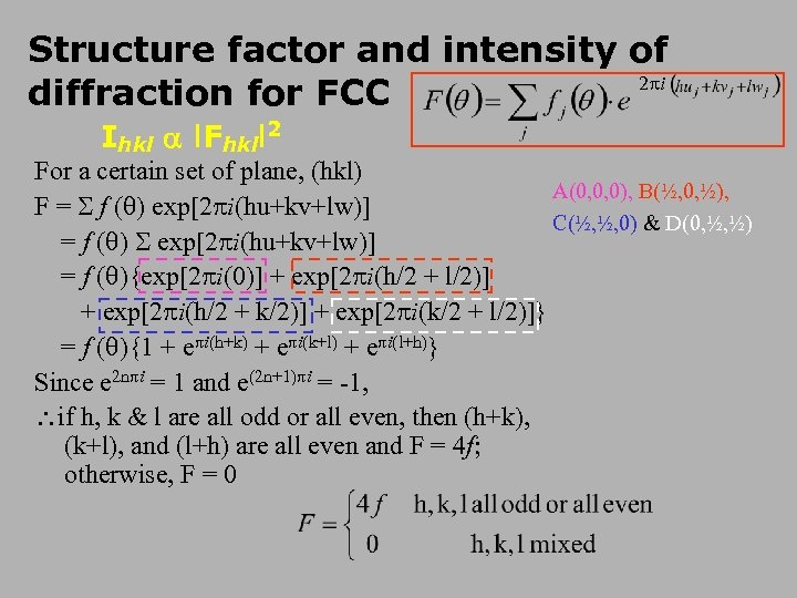 Structure factor and intensity of 2 i diffraction for FCC Ihkl l. Fhkll 2 For a certain set of plane, (hkl) A(0, 0, 0), B(½, 0, ½), F = f ( ) exp[2 i(hu+kv+lw)] C(½, ½, 0) & D(0, ½, ½) = f ( ) exp[2 i(hu+kv+lw)] = f ( ){exp[2 i(0)] + exp[2 i(h/2 + l/2)] + exp[2 i(h/2 + k/2)] + exp[2 i(k/2 + l/2)]} = f ( ){1 + e i(h+k) + e i(k+l) + e i(l+h)} Since e 2 n i = 1 and e(2 n+1) i = -1, if h, k & l are all odd or all even, then (h+k), (k+l), and (l+h) are all even and F = 4 f; otherwise, F = 0
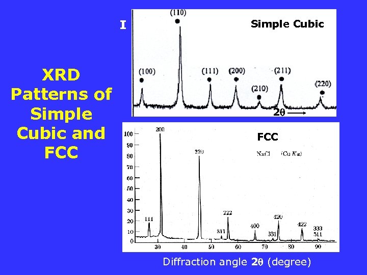 I XRD Patterns of Simple Cubic and FCC Simple Cubic 2 FCC Diffraction angle 2 (degree)
 Diffractions Possibly Present for Cubic Structures
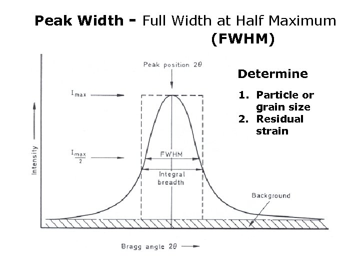 Peak Width - Full Width at Half Maximum (FWHM) Determine 1. Particle or grain size 2. Residual strain
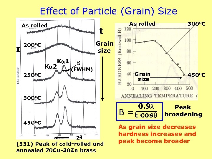 Effect of Particle (Grain) Size As rolled I 300 o. C Grain size 450 o. C Grain size 200 o. C 250 o. C t As rolled K 1 B K 2 (FWHM) 300 o. C 0. 9 B = t cos 450 o. C 2 (331) Peak of cold-rolled annealed 70 Cu-30 Zn brass Peak broadening As grain size decreases hardness increases and peak become broader
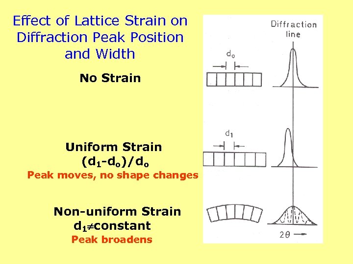 Effect of Lattice Strain on Diffraction Peak Position and Width No Strain Uniform Strain (d 1 -do)/do Peak moves, no shape changes Non-uniform Strain d 1 constant Peak broadens
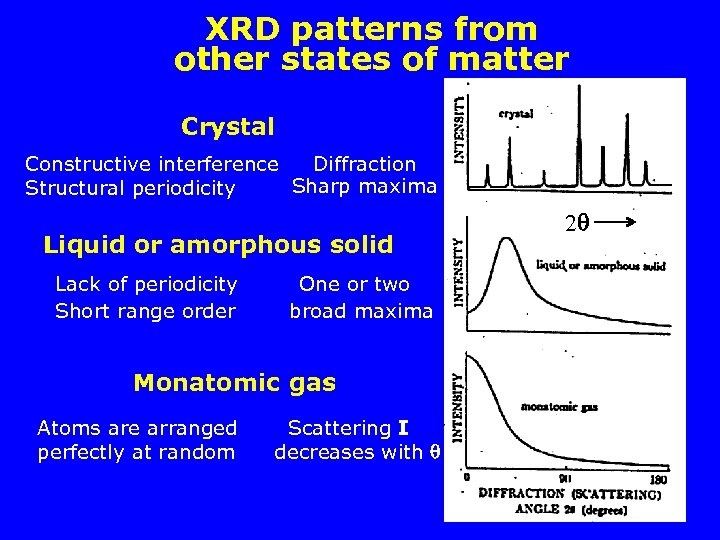 XRD patterns from other states of matter Crystal Constructive interference Diffraction Sharp maxima Structural periodicity Liquid or amorphous solid Lack of periodicity Short range order One or two broad maxima Monatomic gas Atoms are arranged perfectly at random Scattering I decreases with 2
 X-ray Diffraction (XRD) • What is X-ray Diffraction Properties and generation of X-ray • Bragg’s Law • Basics of Crystallography • XRD Pattern • Powder Diffraction • Applications of XRD http: //www. matter. org. uk/diffraction/x-ray/laue_method. htm
![Diffraction of X-rays by Crystals-Laue Method Back-reflection Laue crystal X-ray Film [001] Transmission Laue Diffraction of X-rays by Crystals-Laue Method Back-reflection Laue crystal X-ray Film [001] Transmission Laue](https://present5.com/presentation/d3035167c17b0aa0c9454786a6bfdc2a/image-46.jpg) Diffraction of X-rays by Crystals-Laue Method Back-reflection Laue crystal X-ray Film [001] Transmission Laue crystal Film http: //www. youtube. com/watch? v=Uf. DW 0 -kghm. I at~1: 20 -3: 00 http: //www. youtube. com/watch? v=2 Jwp. Hm. T 6 nt. U
Diffraction of X-rays by Crystals-Laue Method Back-reflection Laue crystal X-ray Film [001] Transmission Laue crystal Film http: //www. youtube. com/watch? v=Uf. DW 0 -kghm. I at~1: 20 -3: 00 http: //www. youtube. com/watch? v=2 Jwp. Hm. T 6 nt. U
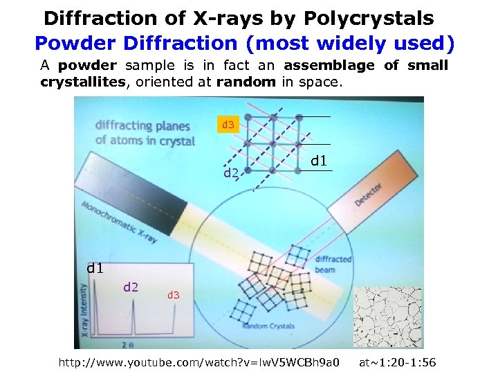 Diffraction of X-rays by Polycrystals Powder Diffraction (most widely used) A powder sample is in fact an assemblage of small crystallites, oriented at random in space. d 3 d 2 d 1 d 2 2 d 3 Polycrystalline sample d 1 Powder sample crystallite http: //www. youtube. com/watch? v=lw. V 5 WCBh 9 a 0 2 at~1: 20 -1: 56
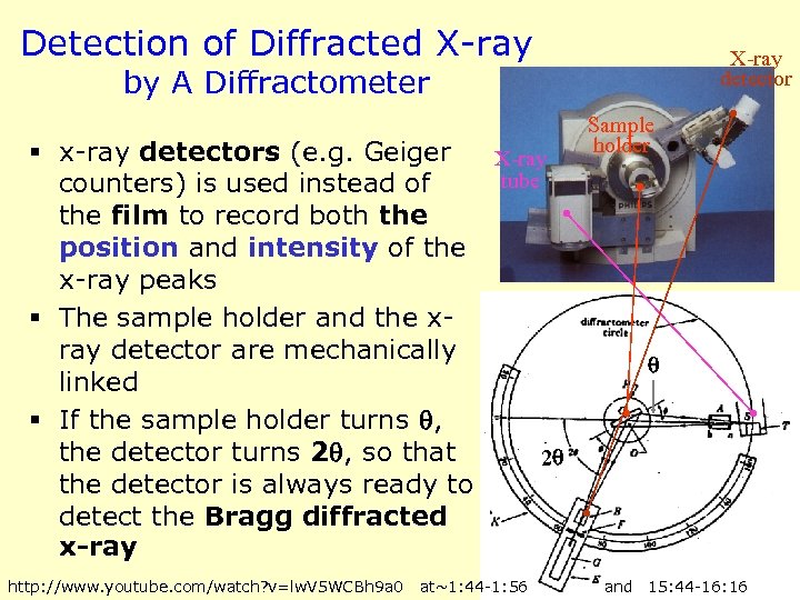 Detection of Diffracted X-ray detector by A Diffractometer § x-ray detectors (e. g. Geiger X-ray tube counters) is used instead of the film to record both the position and intensity of the x-ray peaks § The sample holder and the xray detector are mechanically linked § If the sample holder turns , the detector turns 2 , so that 2 the detector is always ready to detect the Bragg diffracted x-ray http: //www. youtube. com/watch? v=lw. V 5 WCBh 9 a 0 at~1: 44 -1: 56 Sample holder and 15: 44 -16: 16
 Phase Identification One of the most important uses of XRD • • Obtain XRD pattern Measure d-spacings Obtain integrated intensities Compare data with known standards in the JCPDS file, which are for random orientations (there are more than 50, 000 JCPDS cards of inorganic materials).
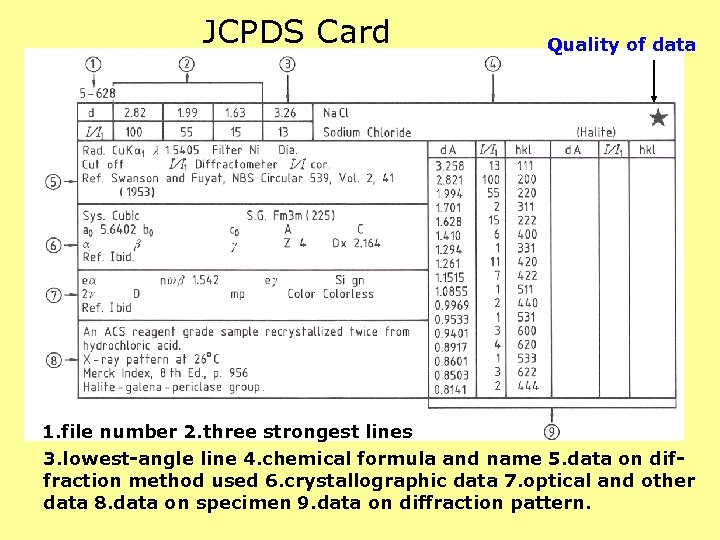 JCPDS Card Quality of data 1. file number 2. three strongest lines 3. lowest-angle line 4. chemical formula and name 5. data on diffraction method used 6. crystallographic data 7. optical and other data 8. data on specimen 9. data on diffraction pattern.
 Other Applications of XRD is a nondestructive technique • To identify crystalline phases • To determine structural properties: Lattice parameters (10 -4Å), strain, grain size, expitaxy, phase composition, preferred orientation order-disorder transformation, thermal expansion • To measure thickness of thin films and multilayers • To determine atomic arrangement • To image and characterize defects Detection limits: ~3% in a two phase mixture; can be ~0. 1% with synchrotron radiation. Lateral resolution: normally none https: //www. youtube. com/watch? v=Cp. JZfe. J 4 po. E phased contrast x-ray imaging https: //www. youtube. com/watch? v=6 POi 6 h 4 df. Vs Determining strain pole figures from diffraction experiments
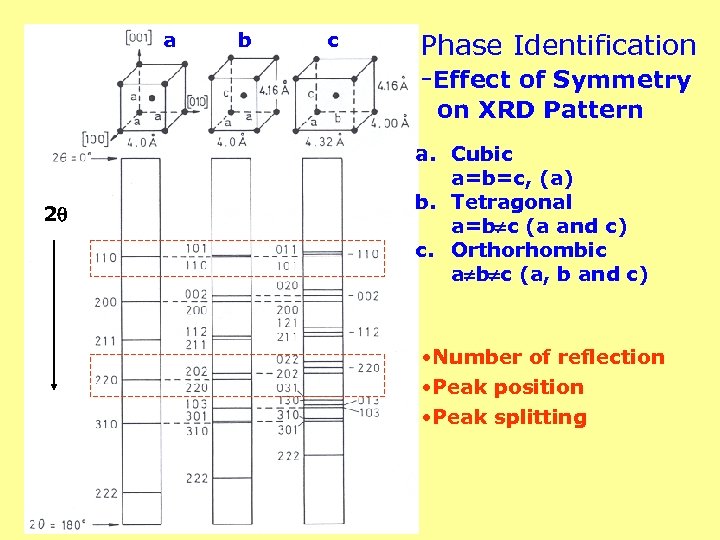 a b c Phase Identification -Effect of Symmetry on XRD Pattern 2 a. Cubic a=b=c, (a) b. Tetragonal a=b c (a and c) c. Orthorhombic a b c (a, b and c) • Number of reflection • Peak position • Peak splitting
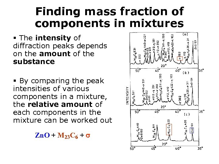 Finding mass fraction of components in mixtures § The intensity of diffraction peaks depends on the amount of the substance § By comparing the peak intensities of various components in a mixture, the relative amount of each components in the mixture can be worked out Zn. O + M 23 C 6 +
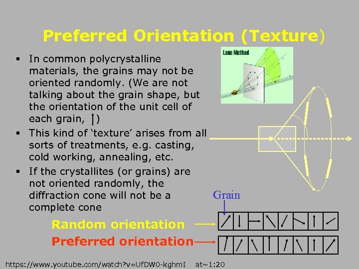 Preferred Orientation (Texture) § In common polycrystalline materials, the grains may not be oriented randomly. (We are not talking about the grain shape, but the orientation of the unit cell of each grain, ) § This kind of ‘texture’ arises from all sorts of treatments, e. g. casting, cold working, annealing, etc. § If the crystallites (or grains) are not oriented randomly, the Grain diffraction cone will not be a complete cone Random orientation Preferred orientation https: //www. youtube. com/watch? v=Uf. DW 0 -kghm. I at~1: 20
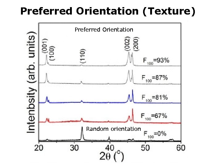 Preferred Orientation (Texture) Preferred Orientation I (110) Random orientation
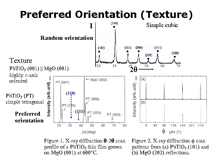 Preferred Orientation (Texture) Simple cubic I Random orientation Texture 20 Pb. Ti. O 3 (001) Mg. O (001) highly c-axis I oriented Pb. Ti. O 3 (PT) simple tetragonal Preferred orientation 30 40 2 50 60 70 I (110) (111) Figure 1. X-ray diffraction -2 scan Figure 2. X-ray diffraction scan profile of a Pb. Ti. O 3 thin film grown patterns from (a) Pb. Ti. O 3 (101) and on Mg. O (001) at 600°C. (b) Mg. O (202) reflections.
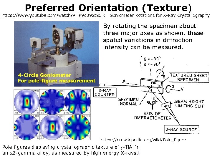 Preferred Orientation (Texture) https: //www. youtube. com/watch? v=R 9 o 39 St. S 5 ik Goniometer Rotations for X-Ray Crystallography By rotating the specimen about three major axes as shown, these spatial variations in diffraction intensity can be measured. 4 -Circle Goniometer For pole-figure measurement https: //en. wikipedia. org/wiki/Pole_figure Pole figures displaying crystallographic texture of -Ti. Al in an 2 -gamma alloy, as measured by high energy X-rays. [
 In Situ XRD Studies • Temperature • Electric Field • Pressure
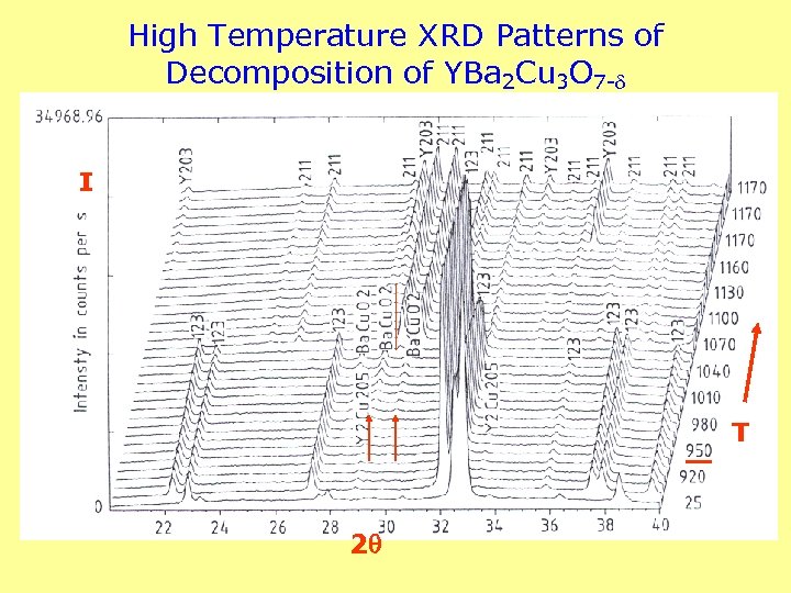 High Temperature XRD Patterns of Decomposition of YBa 2 Cu 3 O 7 - I T 2
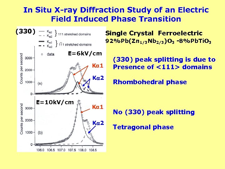 In Situ X-ray Diffraction Study of an Electric Field Induced Phase Transition (330) Single Crystal Ferroelectric 92%Pb(Zn 1/3 Nb 2/3)O 3 -8%Pb. Ti. O 3 E=6 k. V/cm K 1 K 2 E=10 k. V/cm K 1 K 2 (330) peak splitting is due to Presence of <111> domains Rhombohedral phase No (330) peak splitting Tetragonal phase
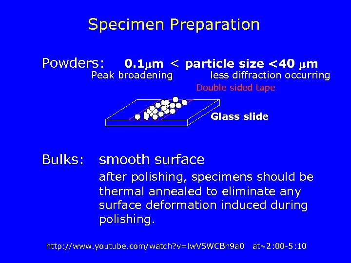 Specimen Preparation Powders: 0. 1 m < particle size <40 m Peak broadening less diffraction occurring Double sided tape Glass slide Bulks: smooth surface after polishing, specimens should be thermal annealed to eliminate any surface deformation induced during polishing. http: //www. youtube. com/watch? v=lw. V 5 WCBh 9 a 0 at~2: 00 -5: 10
 Do review problems for XRD Next Lecture a Transmission Electron Microscopy b


