b3da34cab2f2f781fbcb8e513691eab3.ppt
- Количество слайдов: 23
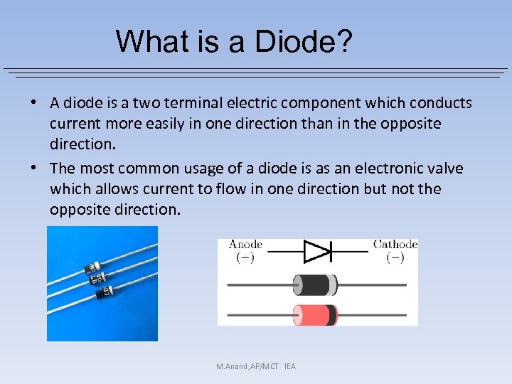 What is a Diode? • A diode is a two terminal electric component which conducts current more easily in one direction than in the opposite direction. • The most common usage of a diode is as an electronic valve which allows current to flow in one direction but not the opposite direction. M. Anand, AP/MCT IEA
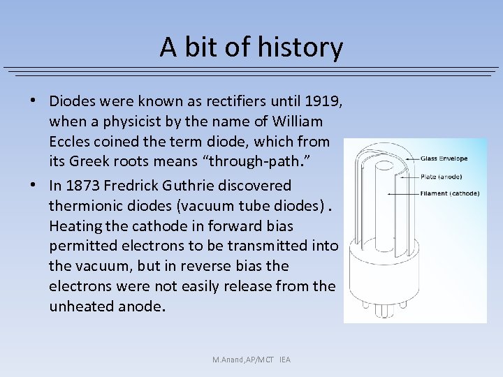 A bit of history • Diodes were known as rectifiers until 1919, when a physicist by the name of William Eccles coined the term diode, which from its Greek roots means “through-path. ” • In 1873 Fredrick Guthrie discovered thermionic diodes (vacuum tube diodes). Heating the cathode in forward bias permitted electrons to be transmitted into the vacuum, but in reverse bias the electrons were not easily release from the unheated anode. M. Anand, AP/MCT IEA
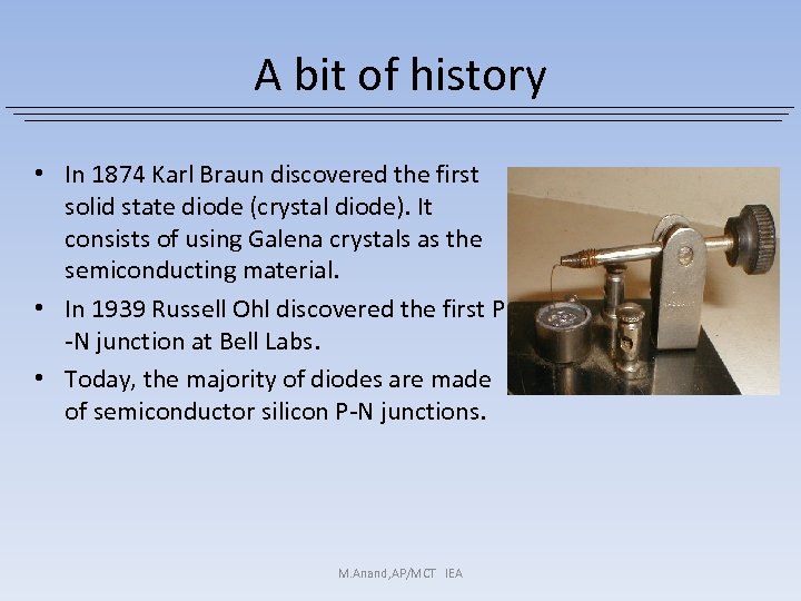 A bit of history • In 1874 Karl Braun discovered the first solid state diode (crystal diode). It consists of using Galena crystals as the semiconducting material. • In 1939 Russell Ohl discovered the first P -N junction at Bell Labs. • Today, the majority of diodes are made of semiconductor silicon P-N junctions. M. Anand, AP/MCT IEA
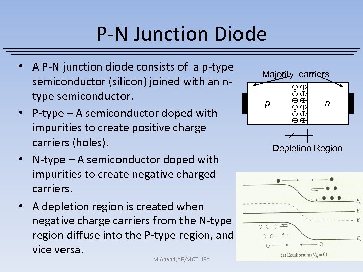 P-N Junction Diode • A P-N junction diode consists of a p-type semiconductor (silicon) joined with an ntype semiconductor. • P-type – A semiconductor doped with impurities to create positive charge carriers (holes). • N-type – A semiconductor doped with impurities to create negative charged carriers. • A depletion region is created when negative charge carriers from the N-type region diffuse into the P-type region, and vice versa. M. Anand, AP/MCT IEA Majority carriers p n Depletion Region
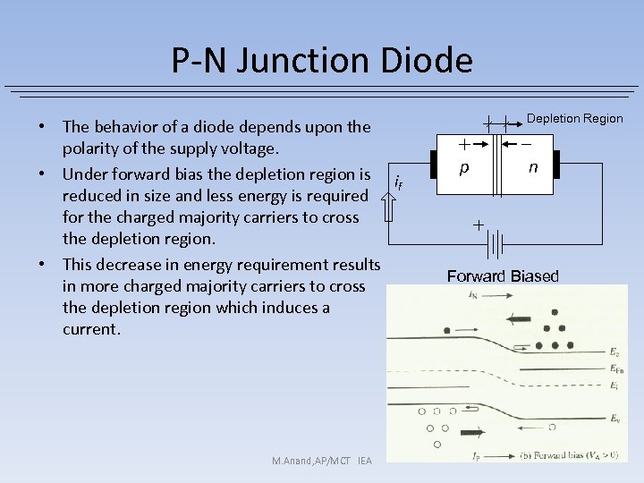 P-N Junction Diode • The behavior of a diode depends upon the polarity of the supply voltage. • Under forward bias the depletion region is i f reduced in size and less energy is required for the charged majority carriers to cross the depletion region. • This decrease in energy requirement results in more charged majority carriers to cross the depletion region which induces a current. M. Anand, AP/MCT IEA Depletion Region p n Forward Biased
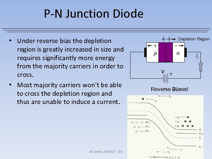 P-N Junction Diode • Under reverse bias the depletion region is greatly increased in size and requires significantly more energy from the majority carriers in order to cross. • Most majority carriers won’t be able to cross the depletion region and thus are unable to induce a current. M. Anand, AP/MCT IEA Depletion Region p n V Reverse Biased ir
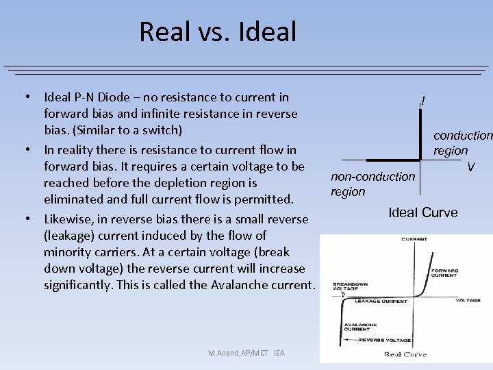 Real vs. Ideal • Ideal P-N Diode – no resistance to current in forward bias and infinite resistance in reverse bias. (Similar to a switch) • In reality there is resistance to current flow in forward bias. It requires a certain voltage to be reached before the depletion region is eliminated and full current flow is permitted. • Likewise, in reverse bias there is a small reverse (leakage) current induced by the flow of minority carriers. At a certain voltage (break down voltage) the reverse current will increase significantly. This is called the Avalanche current. M. Anand, AP/MCT IEA I non-conduction region V Ideal Curve
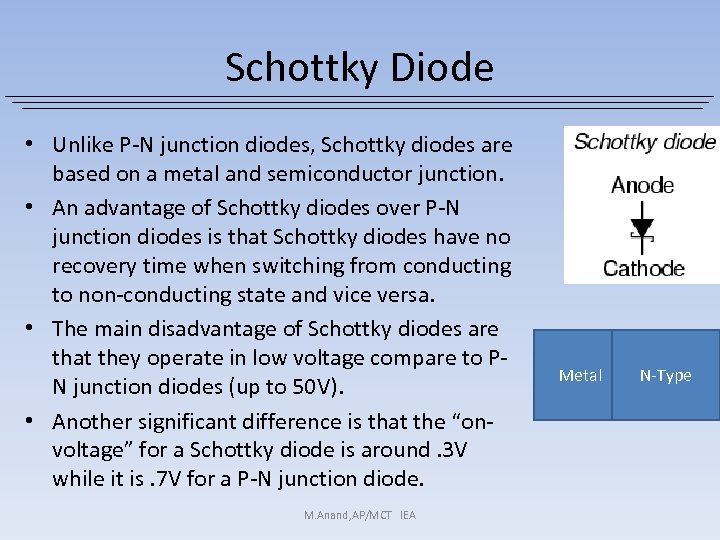 Schottky Diode • Unlike P-N junction diodes, Schottky diodes are based on a metal and semiconductor junction. • An advantage of Schottky diodes over P-N junction diodes is that Schottky diodes have no recovery time when switching from conducting to non-conducting state and vice versa. • The main disadvantage of Schottky diodes are that they operate in low voltage compare to PN junction diodes (up to 50 V). • Another significant difference is that the “onvoltage” for a Schottky diode is around. 3 V while it is. 7 V for a P-N junction diode. M. Anand, AP/MCT IEA Metal N-Type
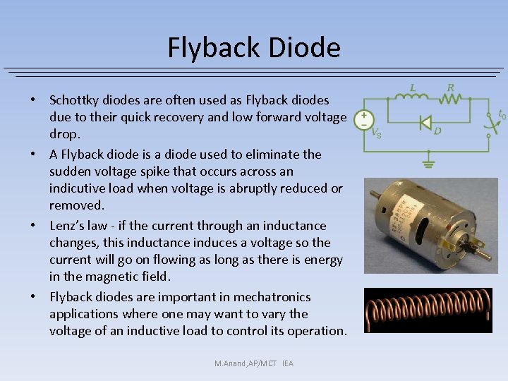 Flyback Diode • Schottky diodes are often used as Flyback diodes due to their quick recovery and low forward voltage drop. • A Flyback diode is a diode used to eliminate the sudden voltage spike that occurs across an indicutive load when voltage is abruptly reduced or removed. • Lenz’s law - if the current through an inductance changes, this inductance induces a voltage so the current will go on flowing as long as there is energy in the magnetic field. • Flyback diodes are important in mechatronics applications where one may want to vary the voltage of an inductive load to control its operation. M. Anand, AP/MCT IEA
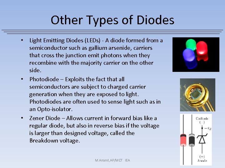 Other Types of Diodes • Light Emitting Diodes (LEDs) - A diode formed from a semiconductor such as gallium arsenide, carriers that cross the junction emit photons when they recombine with the majority carrier on the other side. • Photodiode – Exploits the fact that all semiconductors are subject to charged carrier generation when they are exposed to light. Photodiodes are often used to sense light such as in an Opto-isolator. • Zener Diode – Allows current in forward bias like a regular diode, but also in reverse bias if the voltage is larger than designed voltage, called the Breakdown voltage. M. Anand, AP/MCT IEA
 What are TRIACS? In order to know, we must first look at thyristors… M. Anand, AP/MCT IEA
 What are Thyristors? Class of semiconductor components that can only go in 1 direction. Wide range of devices, SCR (silicon controlled rectifier), SCS (silicon controlled switch), Diacs, Triacs, and Shockley diodes Used in high power switching applications i. e. hundreds of amps / thousands of watts M. Anand, AP/MCT IEA
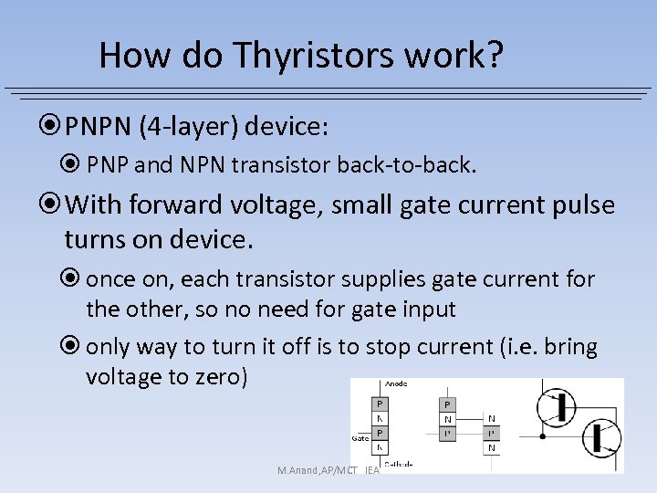 How do Thyristors work? PNPN (4 -layer) device: PNP and NPN transistor back-to-back. With forward voltage, small gate current pulse turns on device. once on, each transistor supplies gate current for the other, so no need for gate input only way to turn it off is to stop current (i. e. bring voltage to zero) M. Anand, AP/MCT IEA
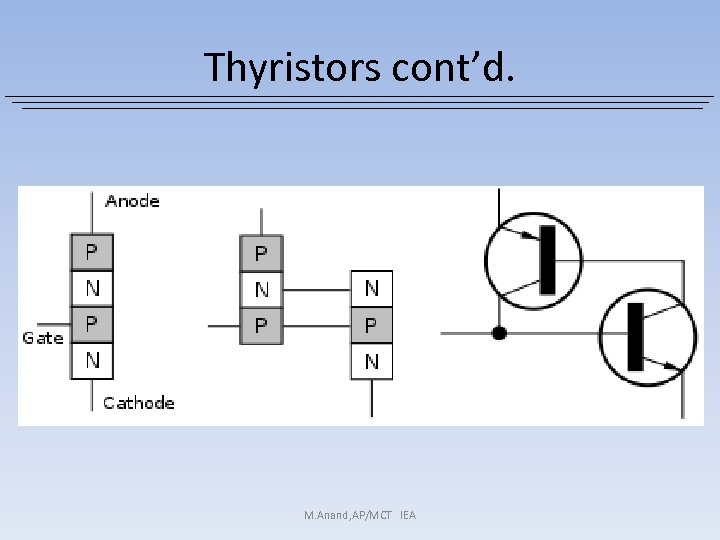 Thyristors cont’d. M. Anand, AP/MCT IEA
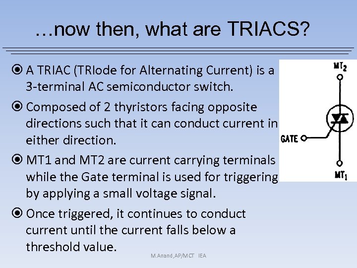 …now then, what are TRIACS? A TRIAC (TRIode for Alternating Current) is a 3 -terminal AC semiconductor switch. Composed of 2 thyristors facing opposite directions such that it can conduct current in either direction. MT 1 and MT 2 are current carrying terminals while the Gate terminal is used for triggering by applying a small voltage signal. Once triggered, it continues to conduct current until the current falls below a threshold value. M. Anand, AP/MCT IEA
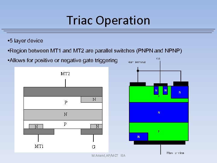 Triac Operation • 5 layer device • Region between MT 1 and MT 2 are parallel switches (PNPN and NPNP) • Allows for positive or negative gate triggering M. Anand, AP/MCT IEA
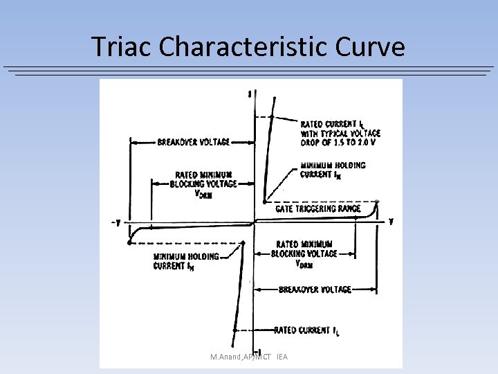 Triac Characteristic Curve M. Anand, AP/MCT IEA
 Triac Characteristic Curve o 1 st quadrant - MT 2 is (+) with respect to MT 1 o VDRM is the break-over voltage of the Triac and the highest voltage that can be blocked o IRDM is the leakage current of the Triac when VDRM is applied to MT 1 and MT 2 o IRDM is several orders of magnitude smaller than the “on” rating M. Anand, AP/MCT IEA
 Triacs Pros: Better than a transistor as it has much better current surge rating – it can handle more current as it simply turns on more Inexpensive compared to relays Cons: Can't manually control turn-off with the gate; must turn off by stopping current through the device via the terminals. Specs to buy one: Gate signal requirements Voltage drop Steady-state/holding current (continuously handle) Peak current (maximum amount to handle surge) M. Anand, AP/MCT IEA
 Triac Applications High Power TRIACS • Switching for AC circuits, allowing the control of very large power flows with milliampere-scale control currents • Can eliminate mechanical wear in a relay Low Power TRIACS • Light bulb dimmers (done by applying power later in the AC cycle aka PWM of AC wave) • Motor speed controls for electric fans and other AC motors, and heaters • Modern computerized control circuits in household appliances M. Anand, AP/MCT IEA
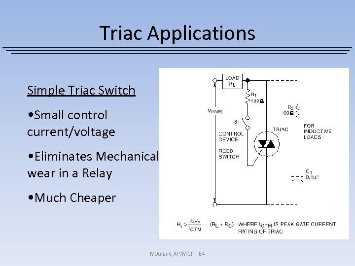 Triac Applications Simple Triac Switch • Small control current/voltage • Eliminates Mechanical wear in a Relay • Much Cheaper M. Anand, AP/MCT IEA
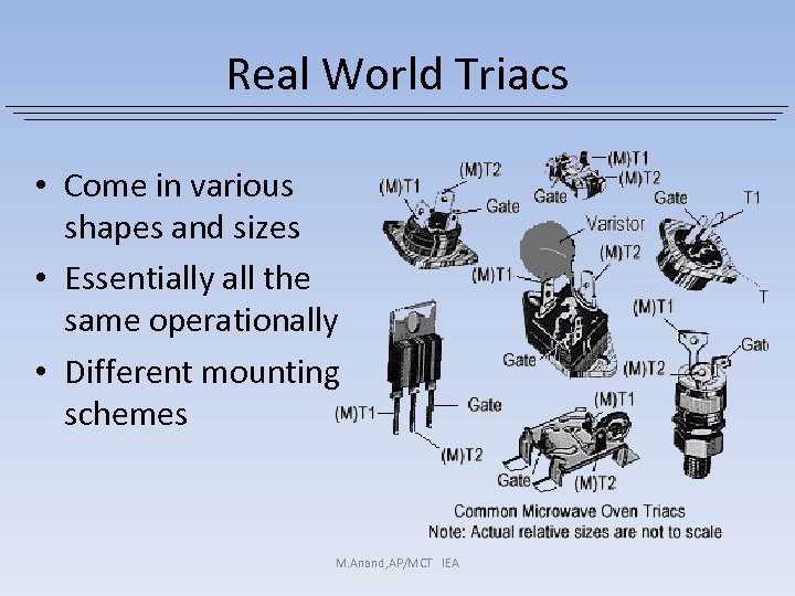 Real World Triacs • Come in various shapes and sizes • Essentially all the same operationally • Different mounting schemes M. Anand, AP/MCT IEA
 QUESTIONS? M. Anand, AP/MCT IEA


