de13409a9a3a29997b5909531569b9ea.ppt
- Количество слайдов: 25
What Does SPAD Afterpulsing Actually Tell Us About Defects in In. P? Mark Itzler, Mark Entwistle, and Xudong Jiang SPW 2011 – June 2011
Presentation Outline · 50 MHz photon counting with RF matched delay line scheme · Afterpulse probability (APP) dependence on hold-off time · Fitting of APP data w inadequacy of legacy approach assuming one or few traps w new fitting based on broad trap distribution · Implications of APP modeling for trap distributions · Summary SPW 2011 – June 2011 Princeton Lightwave Inc. 2
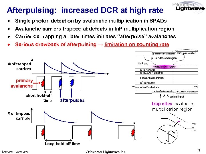
Afterpulsing: increased DCR at high rate · · Single photon detection by avalanche multiplication in SPADs Avalanche carriers trapped at defects in In. P multiplication region Carrier de-trapping at later times initiates “afterpulse” avalanches Serious drawback of afterpulsing → limitation on counting rate # of trapped carriers primary avalanche short hold-off time afterpulses trap sites located in multiplication region # of trapped carriers Ec Ev Long hold-off time SPW 2011 – June 2011 Princeton Lightwave Inc. 3
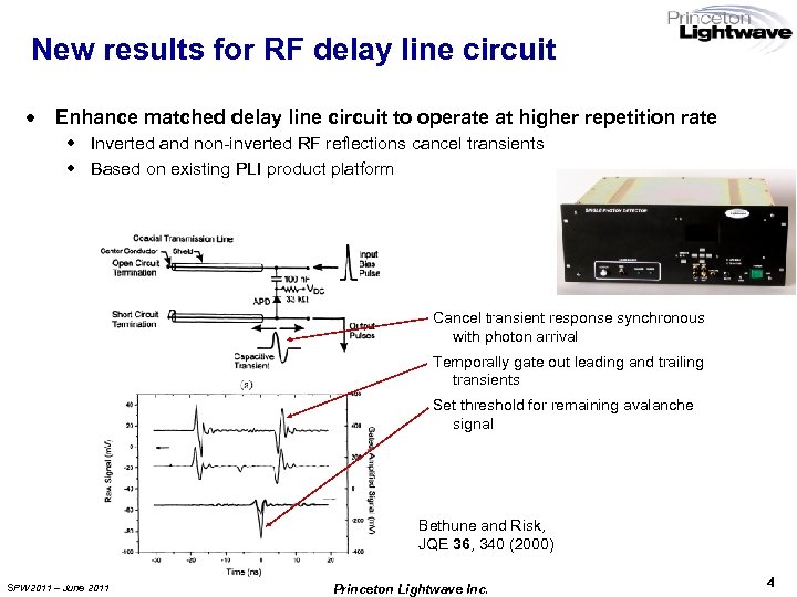
New results for RF delay line circuit · Enhance matched delay line circuit to operate at higher repetition rate w Inverted and non-inverted RF reflections cancel transients w Based on existing PLI product platform Cancel transient response synchronous with photon arrival Temporally gate out leading and trailing transients Set threshold for remaining avalanche signal Bethune and Risk, JQE 36, 340 (2000) SPW 2011 – June 2011 Princeton Lightwave Inc. 4
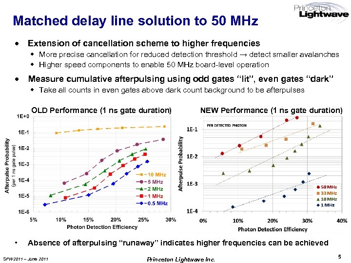
Matched delay line solution to 50 MHz · Extension of cancellation scheme to higher frequencies w More precise cancellation for reduced detection threshold → detect smaller avalanches w Higher speed components to enable 50 MHz board-level operation · Measure cumulative afterpulsing using odd gates “lit”, even gates “dark” w Take all counts in even gates above dark count background to be afterpulses OLD Performance (1 ns gate duration) • NEW Performance (1 ns gate duration) Absence of afterpulsing “runaway” indicates higher frequencies can be achieved SPW 2011 – June 2011 Princeton Lightwave Inc. 5
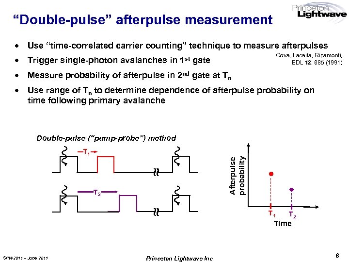
“Double-pulse” afterpulse measurement · Use “time-correlated carrier counting” technique to measure afterpulses · Trigger single-photon avalanches in 1 st gate · Measure probability of afterpulse in 2 nd gate at Tn · Use range of Tn to determine dependence of afterpulse probability on time following primary avalanche Cova, Lacaita, Ripamonti, EDL 12, 685 (1991) T 1 ≈ T 2 Afterpulse probability Double-pulse (“pump-probe”) method ≈ T 1 T 2 Time SPW 2011 – June 2011 Princeton Lightwave Inc. 6
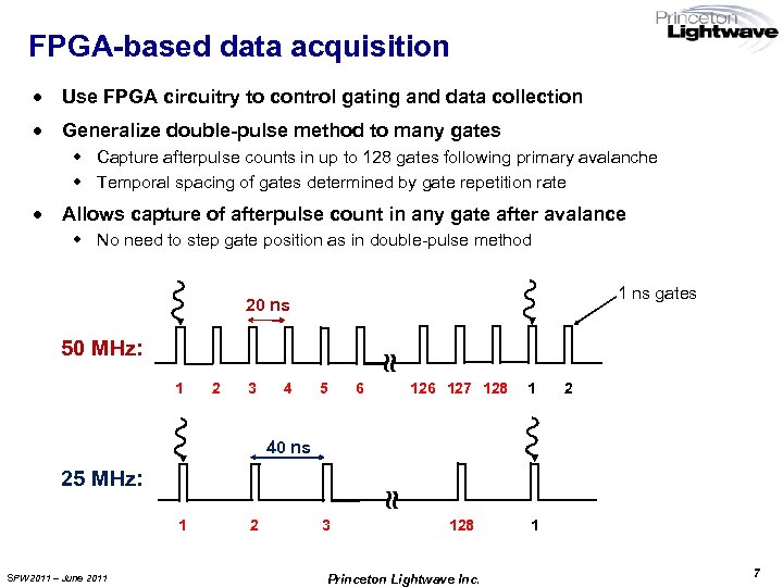
FPGA-based data acquisition · Use FPGA circuitry to control gating and data collection · Generalize double-pulse method to many gates w Capture afterpulse counts in up to 128 gates following primary avalanche w Temporal spacing of gates determined by gate repetition rate · Allows capture of afterpulse count in any gate after avalance w No need to step gate position as in double-pulse method 1 ns gates 20 ns ≈ 50 MHz: 1 2 3 4 5 6 127 128 1 2 40 ns ≈ 25 MHz: 1 SPW 2011 – June 2011 2 3 128 Princeton Lightwave Inc. 1 7
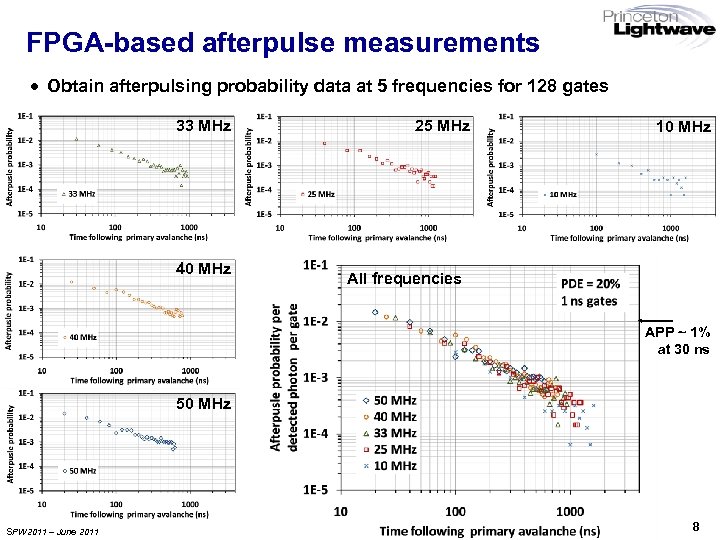
FPGA-based afterpulse measurements · Obtain afterpulsing probability data at 5 frequencies for 128 gates 33 MHz 40 MHz 25 MHz 10 MHz All frequencies APP ~ 1% at 30 ns 50 MHz SPW 2011 – June 2011 Princeton Lightwave Inc. 8
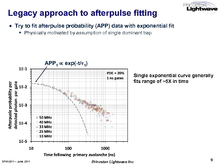
Legacy approach to afterpulse fitting · Try to fit afterpulse probability (APP) data with exponential fit w Physically motivated by assumption of single dominant trap APP 1 exp(-t/τ1) Single exponential curve generally fits range of ~5 X in time SPW 2011 – June 2011 Princeton Lightwave Inc. 9
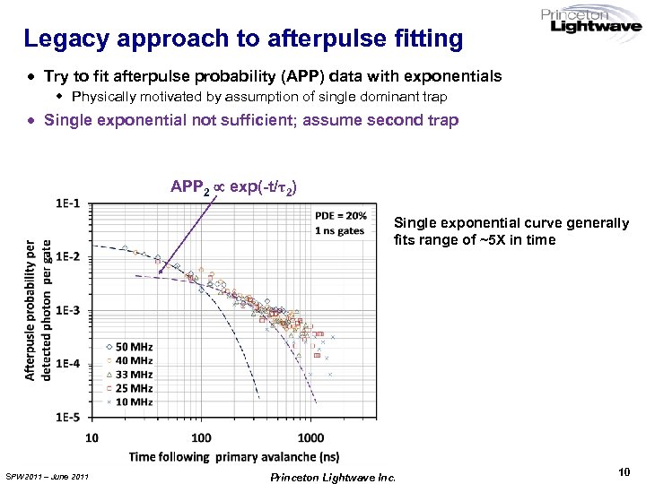
Legacy approach to afterpulse fitting · Try to fit afterpulse probability (APP) data with exponentials w Physically motivated by assumption of single dominant trap · Single exponential not sufficient; assume second trap APP 2 exp(-t/τ2) Single exponential curve generally fits range of ~5 X in time SPW 2011 – June 2011 Princeton Lightwave Inc. 10
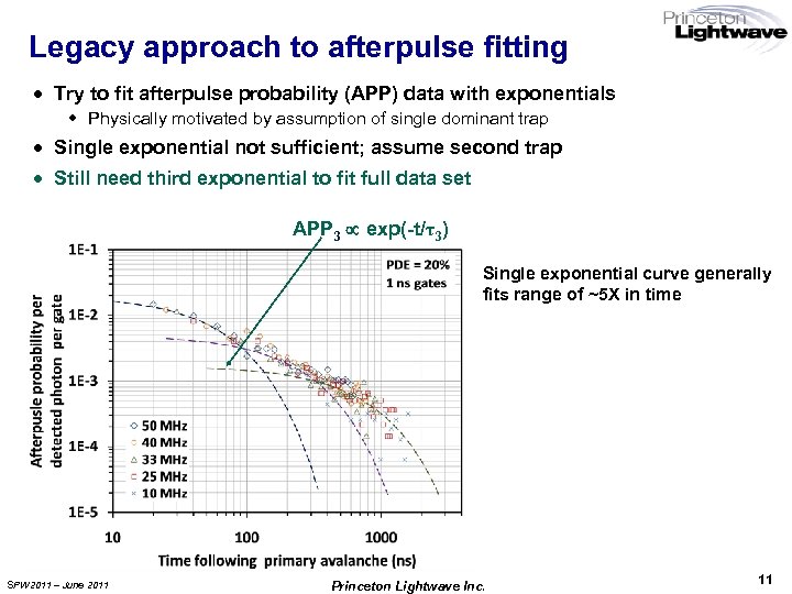
Legacy approach to afterpulse fitting · Try to fit afterpulse probability (APP) data with exponentials w Physically motivated by assumption of single dominant trap · Single exponential not sufficient; assume second trap · Still need third exponential to fit full data set APP 3 exp(-t/τ3) Single exponential curve generally fits range of ~5 X in time SPW 2011 – June 2011 Princeton Lightwave Inc. 11
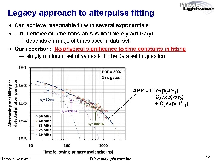
Legacy approach to afterpulse fitting · Can achieve reasonable fit with several exponentials · …but choice of time constants is completely arbitrary! → depends on range of times used in data set · Our assertion: No physical significance to time constants in fitting → simply minimum set of values to fit the data set in question APP = C 1 exp(-t/τ1) + C 2 exp(-t/τ2) + C 3 exp(-t/τ3) SPW 2011 – June 2011 Princeton Lightwave Inc. 12
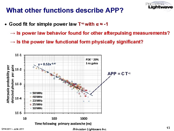
What other functions describe APP? · Good fit for simple power law T-α with α ≈ -1 → Is power law behavior found for other afterpulsing measurements? → Is the power law functional form physically significant? APP = C T-α SPW 2011 – June 2011 Princeton Lightwave Inc. 13
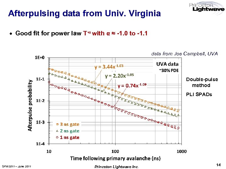
Afterpulsing data from Univ. Virginia · Good fit for power law T-α with α ≈ -1. 0 to -1. 1 data from Joe Campbell, UVA Double-pulse method PLI SPADs SPW 2011 – June 2011 Princeton Lightwave Inc. 14
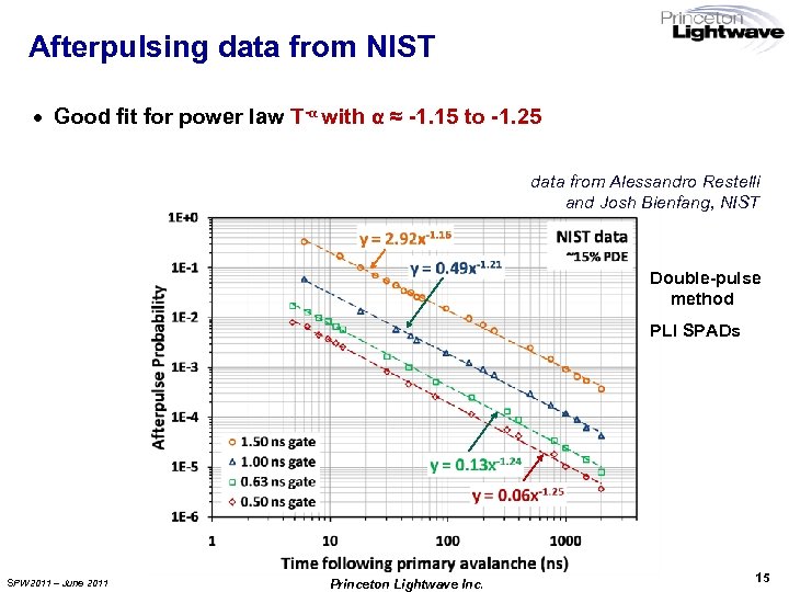
Afterpulsing data from NIST · Good fit for power law T-α with α ≈ -1. 15 to -1. 25 data from Alessandro Restelli and Josh Bienfang, NIST Double-pulse method PLI SPADs SPW 2011 – June 2011 Princeton Lightwave Inc. 15
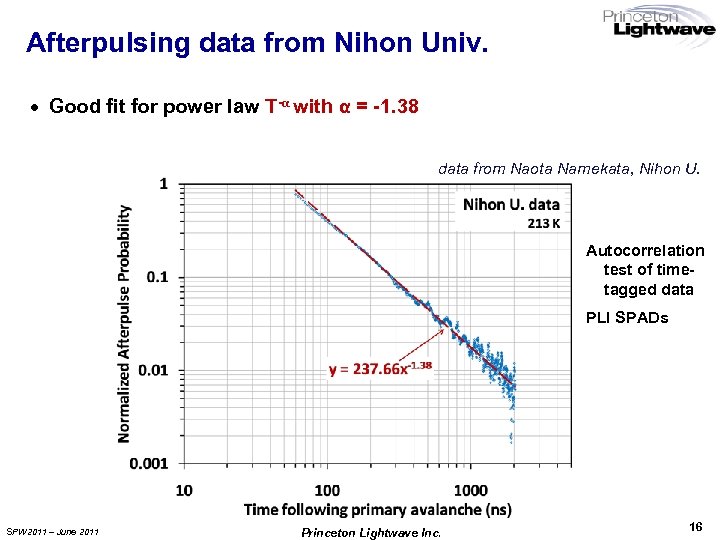
Afterpulsing data from Nihon Univ. · Good fit for power law T-α with α = -1. 38 data from Naota Namekata, Nihon U. Autocorrelation test of timetagged data PLI SPADs SPW 2011 – June 2011 Princeton Lightwave Inc. 16
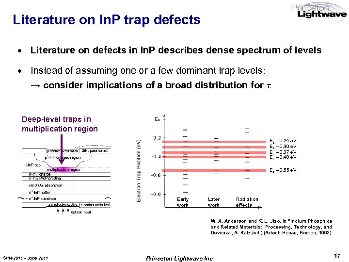
Literature on In. P trap defects · Literature on defects in In. P describes dense spectrum of levels · Instead of assuming one or a few dominant trap levels: → consider implications of a broad distribution for τ Deep-level traps in multiplication region Ec – 0. 24 e. V Ec – 0. 30 e. V Ec – 0. 37 e. V Ec – 0. 40 e. V Ec – 0. 55 e. V Early work Later work Radiation effects W. A. Anderson and K. L. Jiao, in “Indium Phosphide and Related Materials: Processing, Technology, and Devices”, A. Katz (ed. ) (Artech House, Boston, 1992) SPW 2011 – June 2011 Princeton Lightwave Inc. 17
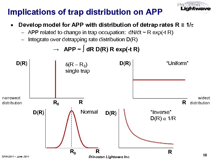
Implications of trap distribution on APP · Develop model for APP with distribution of detrap rates R ≡ 1/τ – APP related to change in trap occupation: d. N/dt ~ R exp(-t R) – Integrate over detrapping rate distribution D(R) → APP ~ ∫ d. R D(R) R exp(-t R) D(R) narrowest distribution “Uniform” R R 0 R Normal D(R) SPW 2011 – June 2011 D(R) δ(R – R 0) single trap R 0 D(R) R Princeton Lightwave Inc. widest distribution “Inverse” D(R) α 1/R R 18
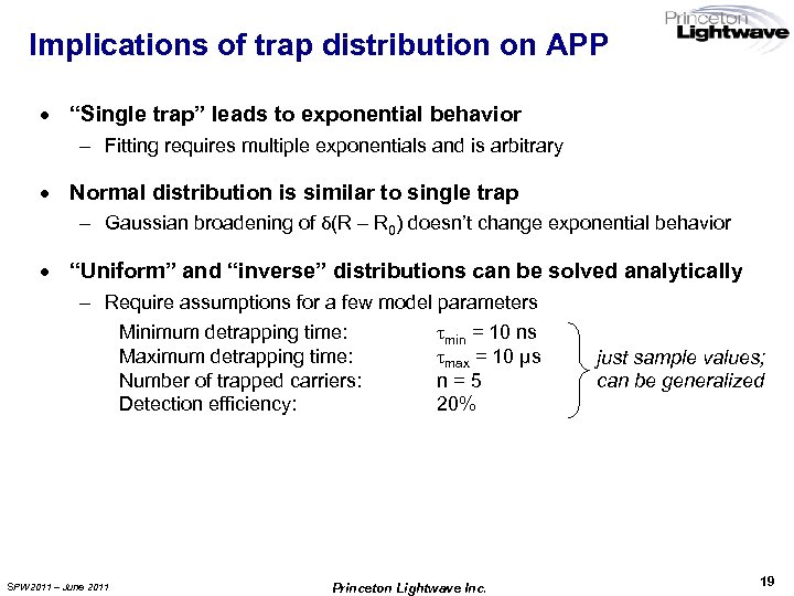
Implications of trap distribution on APP · “Single trap” leads to exponential behavior – Fitting requires multiple exponentials and is arbitrary · Normal distribution is similar to single trap – Gaussian broadening of δ(R – R 0) doesn’t change exponential behavior · “Uniform” and “inverse” distributions can be solved analytically – Require assumptions for a few model parameters Minimum detrapping time: τmin = 10 ns Maximum detrapping time: τmax = 10 µs Number of trapped carriers: n=5 Detection efficiency: 20% SPW 2011 – June 2011 Princeton Lightwave Inc. just sample values; can be generalized 19
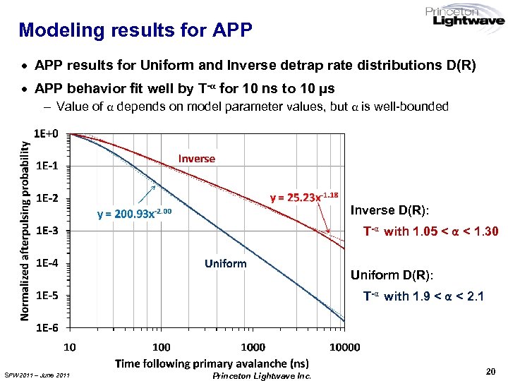
Modeling results for APP · APP results for Uniform and Inverse detrap rate distributions D(R) · APP behavior fit well by T-α for 10 ns to 10 µs – Value of α depends on model parameter values, but α is well-bounded Inverse D(R): T-α with 1. 05 < α < 1. 30 Uniform D(R): T-α with 1. 9 < α < 2. 1 SPW 2011 – June 2011 Princeton Lightwave Inc. 20
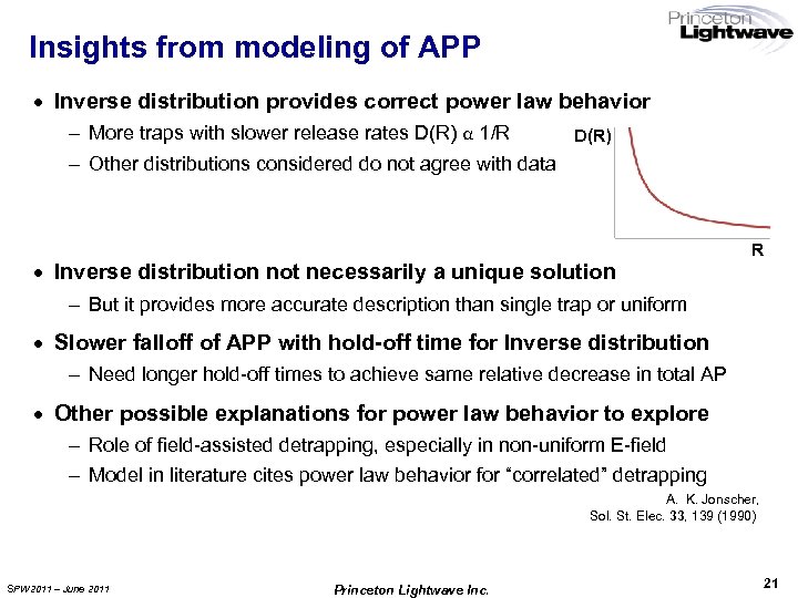
Insights from modeling of APP · Inverse distribution provides correct power law behavior – More traps with slower release rates D(R) α 1/R D(R) – Other distributions considered do not agree with data · Inverse distribution not necessarily a unique solution R – But it provides more accurate description than single trap or uniform · Slower falloff of APP with hold-off time for Inverse distribution – Need longer hold-off times to achieve same relative decrease in total AP · Other possible explanations for power law behavior to explore – Role of field-assisted detrapping, especially in non-uniform E-field – Model in literature cites power law behavior for “correlated” detrapping A. K. Jonscher, Sol. St. Elec. 33, 139 (1990) SPW 2011 – June 2011 Princeton Lightwave Inc. 21
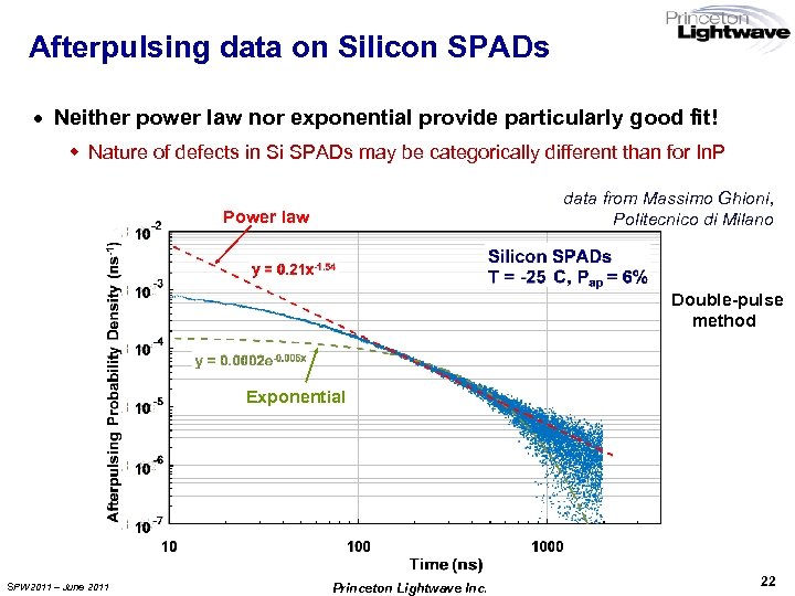
Afterpulsing data on Silicon SPADs · Neither power law nor exponential provide particularly good fit! w Nature of defects in Si SPADs may be categorically different than for In. P data from Massimo Ghioni, Politecnico di Milano Power law Double-pulse method Exponential SPW 2011 – June 2011 Princeton Lightwave Inc. 22
Summary · Reached 50 MHz photon counting with RF matched delay line scheme w Significant further repetition rate increases should be feasible · Fitting of APP data with multiple exponentials not physically meaningful w Extracted detrapping times are arbitrary, depend on hold-off times used w Literature on defects in In. P suggests possibility of broad distribution of defects · Consistent power law behavior of APP data found by various groups w APP vs. time T described by T-α with α ~ 1. 2 ± 0. 2 · Assumption of “inverse” distribution D(R) α 1/R for detrapping rate R provides best description of data among distributions considered so far w Not unique, but establishes general behavior w May be other models that predict power law APP behavior for dominant trap w Further modeling can predict behavior for different operating conditions SPW 2011 – June 2011 Princeton Lightwave Inc. 23

BACK-UP SLIDES SPW 2011 – June 2011 Princeton Lightwave Inc. 24
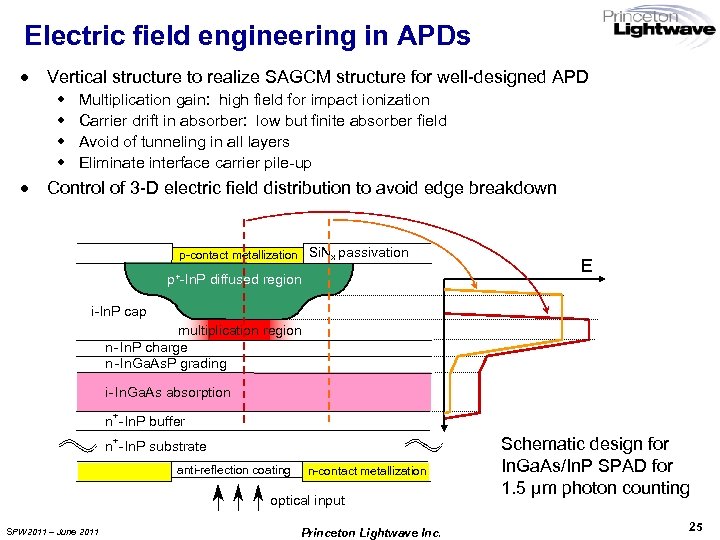
Electric field engineering in APDs · Vertical structure to realize SAGCM structure for well-designed APD w w · Multiplication gain: high field for impact ionization Carrier drift in absorber: low but finite absorber field Avoid of tunneling in all layers Eliminate interface carrier pile-up Control of 3 -D electric field distribution to avoid edge breakdown p-contact metallization Si. Nx passivation p+-In. P diffused region E i-In. P cap multiplication region n- In. P charge n -In. Ga. As. P grading i- In. Ga. As absorption + n -In. P buffer + n -In. P substrate anti-reflection coating n-contact metallization optical input SPW 2011 – June 2011 Princeton Lightwave Inc. Schematic design for In. Ga. As/In. P SPAD for 1. 5 μm photon counting 25
de13409a9a3a29997b5909531569b9ea.ppt