2384f1e941d6bc34763b82cfd739a982.ppt
- Количество слайдов: 54
 VLSI/SOC Design Methodologies and Challenges Dr. Chia-Jiu Wang University of Colorado at Colorado Springs Department of Electrical and Computer Engineering 1
 Outline: Microelectronics Industry Evolution Cell-based Design Semi-custom Design Challenge Examples Wire and crosstalk Low power design Verilog Examples: a processor 2
 Evolution (revolution) of IC design • • • The micro electronics industry only stays well alive (continuous growth) because of this rapid progress. (performance doubles every ~2 years) – This rate of progress MUST be maintained to keep IC industry in good shape. – The life time of a technology generation is ~5 years Production is cheap in large quantities because of lithographic processing (“like printing stamps”) Design is complicated and very expensive – (design mistakes costs lot of time and money) If cars had the same rate of improvement as integrated circuits a car today could: Drive at the speed of light Drive years on one single tank of gasoline Transport a whole city in one car 3
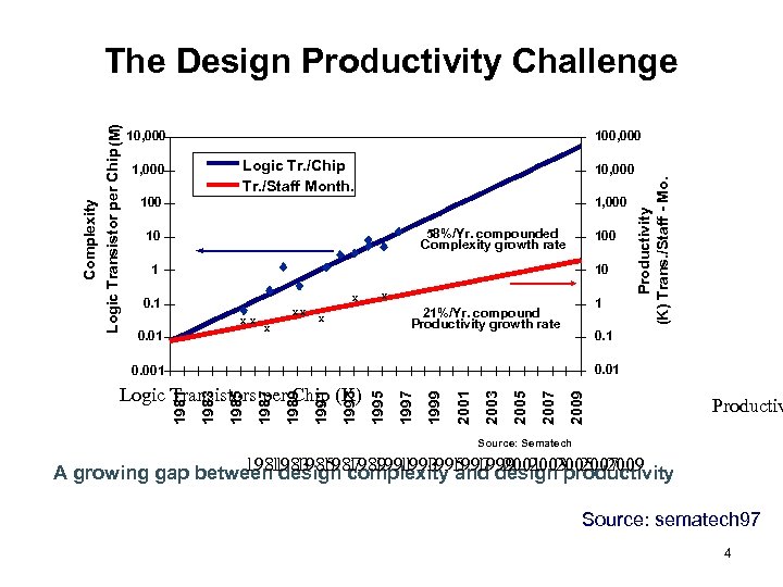 10, 000 100, 000, 000 Logic Tr. /Chip Tr. /Staff Month. 1, 000, 000 10, 000 100, 000 Productivity (K) Trans. /Staff - Mo. Complexity Logic Transistor per Chip (M) The Design Productivity Challenge 1, 000, 000 58%/Yr. compounded Complexity growth rate 10 10, 000 100, 000 1 1, 000 10 10, 000 x 0. 1 100 xx 0. 01 10 xx x x 1 1, 000 21%/Yr. compound Productivity growth rate x 0. 1 100 0. 01 10 2009 2007 2005 2003 2001 1999 1997 1993 1991 1989 1987 1985 1983 1981 Logic Transistors per Chip (K) 1995 0. 001 1 Productiv Source: Sematech 1981 1985 complexity 1997 design 2005 2009 A growing gap between 1983 1987 1991 1995 1999 2003 2007 design 1989 1993 and 2001 productivity Source: sematech 97 4
 How to put together millions of transistors and make it work ? • • Well chosen design/Implementation methodologies Well chosen architectures Extensive use of power full CAE tools Strict design management Well chosen testing methodologies Design re-use One can not use same design methodologies and architectures when complexity increases orders of magnitude 5
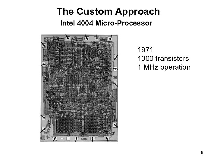 The Custom Approach Intel 4004 Micro-Processor 1971 1000 transistors 1 MHz operation 6
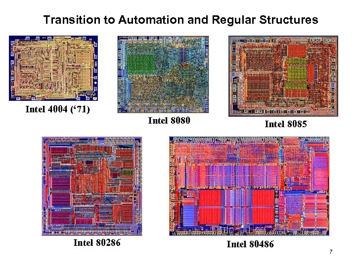 Transition to Automation and Regular Structures Intel 4004 (‘ 71) Intel 80286 Intel 8080 Intel 8085 Intel 80486 7
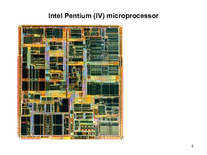 Intel Pentium (IV) microprocessor 8
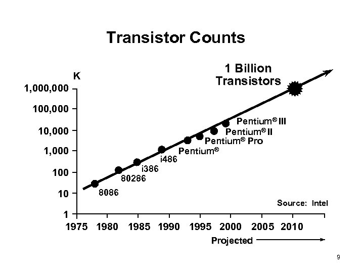 Transistor Counts 1 Billion Transistors K 1, 000 100, 000 1, 000 i 386 80286 100 10 i 486 Pentium® III Pentium® Pro Pentium® 8086 Source: Intel 1 1975 1980 1985 1990 1995 2000 2005 2010 Projected 9
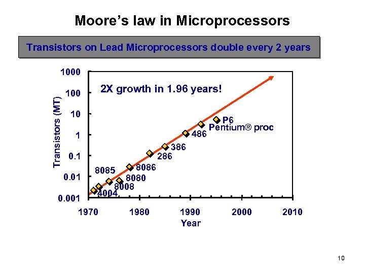 Moore’s law in Microprocessors Transistors on Lead Microprocessors double every 2 years Transistors (MT) 1000 2 X growth in 1. 96 years! 100 10 486 1 386 286 0. 1 0. 01 P 6 Pentium® proc 8086 8080 8008 4004 8085 0. 001 1970 1980 1990 Year 2000 2010 10
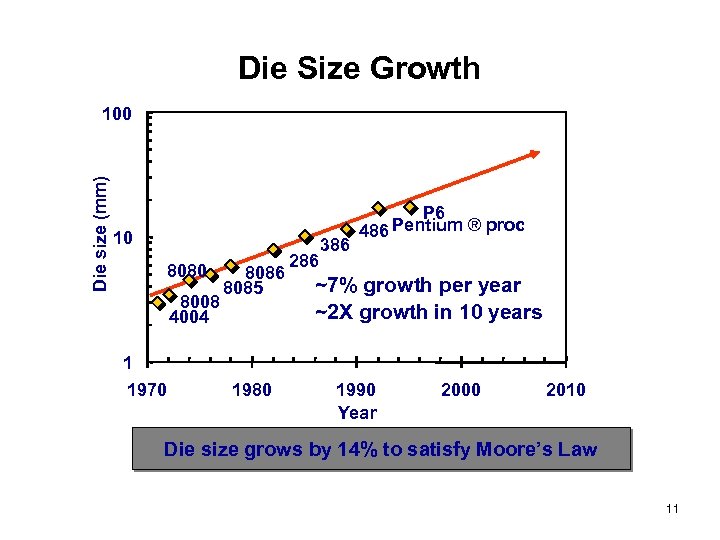 Die Size Growth Die size (mm) 100 10 8080 8008 4004 1 1970 8086 8085 1980 286 386 P 6 Pentium ® proc 486 ~7% growth per year ~2 X growth in 10 years 1990 Year 2000 2010 Die size grows by 14% to satisfy Moore’s Law 11
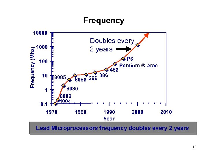 Frequency (Mhz) 10000 Doubles every 2 years 1000 10 8085 1 0. 1 1970 8086 286 386 486 P 6 Pentium ® proc 8080 8008 4004 1980 1990 Year 2000 2010 Lead Microprocessors frequency doubles every 2 years 12
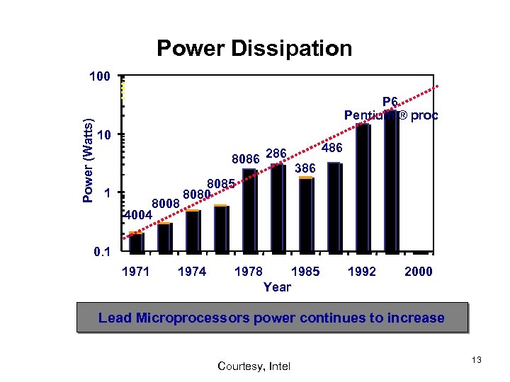 Power Dissipation Power (Watts) 100 P 6 Pentium ® proc 10 8086 286 1 8008 4004 486 386 8085 8080 0. 1 1974 1978 1985 1992 2000 Year Lead Microprocessors power continues to increase Courtesy, Intel 13
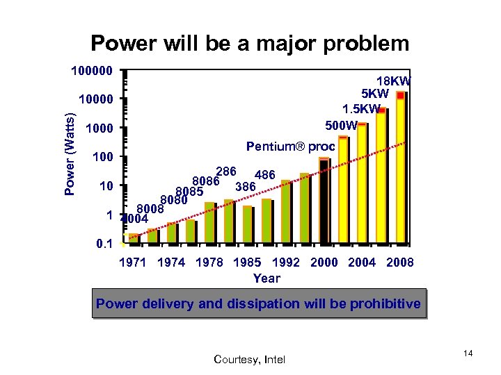 Power will be a major problem 100000 18 KW 5 KW 1. 5 KW 500 W Power (Watts) 10000 100 Pentium® proc 286 486 8086 386 10 8085 8080 8008 1 4004 0. 1 1974 1978 1985 1992 2000 2004 2008 Year Power delivery and dissipation will be prohibitive Courtesy, Intel 14
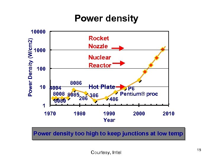 Power density Power Density (W/cm 2) 10000 100 Rocket Nozzle Nuclear Reactor 8086 10 4004 Hot Plate P 6 8008 8085 Pentium® proc 386 286 486 8080 1 1970 1980 1990 2000 2010 Year Power density too high to keep junctions at low temp Courtesy, Intel 15
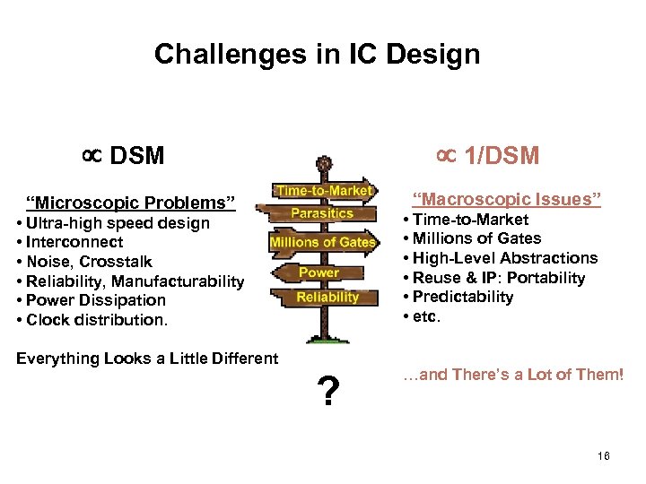 Challenges in IC Design µ DSM µ 1/DSM “Macroscopic Issues” “Microscopic Problems” • Time-to-Market • Millions of Gates • High-Level Abstractions • Reuse & IP: Portability • Predictability • etc. • Ultra-high speed design • Interconnect • Noise, Crosstalk • Reliability, Manufacturability • Power Dissipation • Clock distribution. Everything Looks a Little Different ? …and There’s a Lot of Them! 16
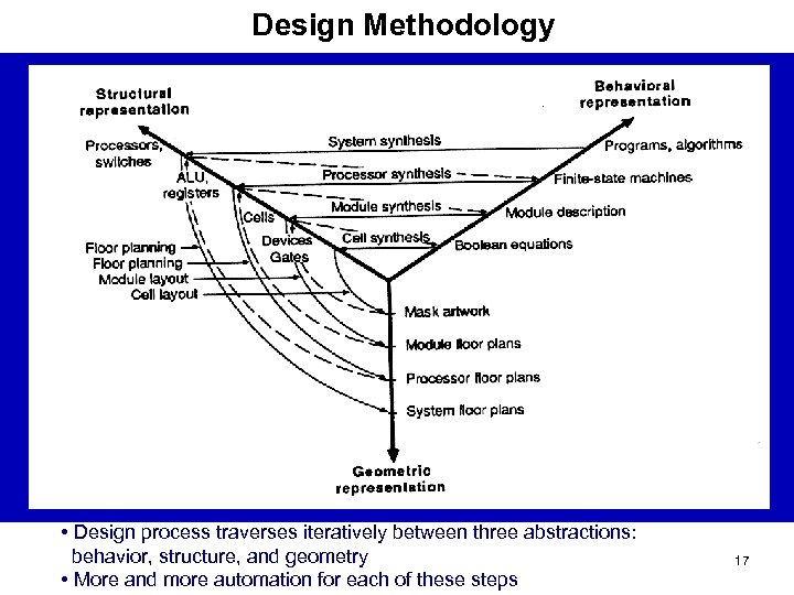 Design Methodology • Design process traverses iteratively between three abstractions: behavior, structure, and geometry • More and more automation for each of these steps 17
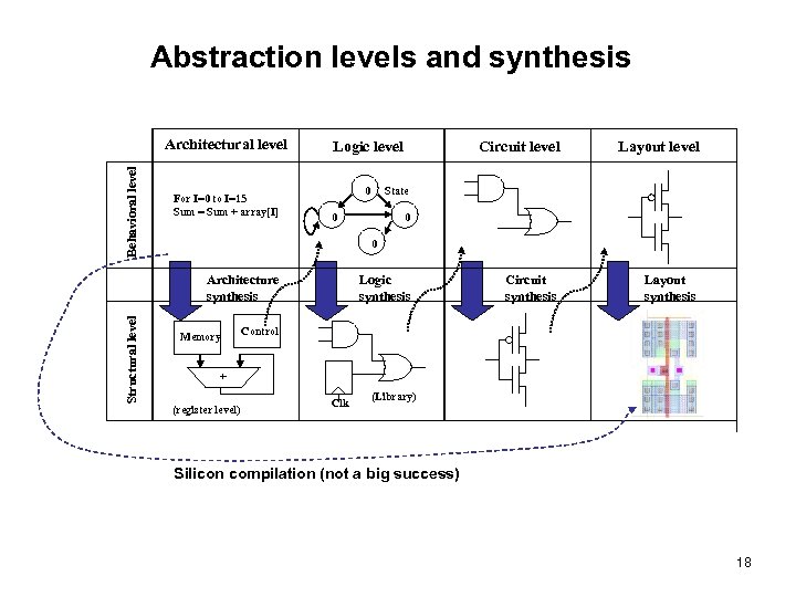 Abstraction levels and synthesis Behavioral level Architectural level For I=0 to I=15 Sum = Sum + array[I] Logic level 0 Layout level Circuit synthesis Layout synthesis State 0 0 0 Architecture synthesis Structural level Circuit level Memory Logic synthesis Control + (register level) Clk (Library) Silicon compilation (not a big success) 18
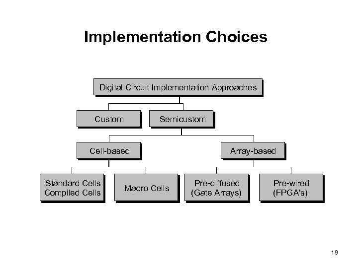 Implementation Choices Digital Circuit Implementation Approaches Custom Semicustom Cell-based Standard Cells Compiled Cells Macro Cells Array-based Pre-diffused (Gate Arrays) Pre-wired (FPGA's) 19
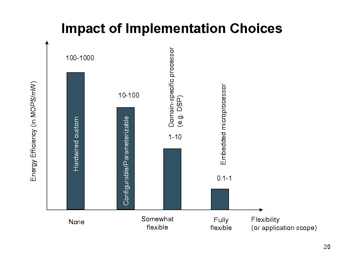 None 100 -1000 10 -100 1 -10 Somewhat flexible Embedded microprocessor Domain-specific processor (e. g. DSP) Configurable/Parameterizable Hardwired custom Energy Efficiency (in MOPS/m. W) Impact of Implementation Choices 0. 1 -1 Fully flexible Flexibility (or application scope) 20
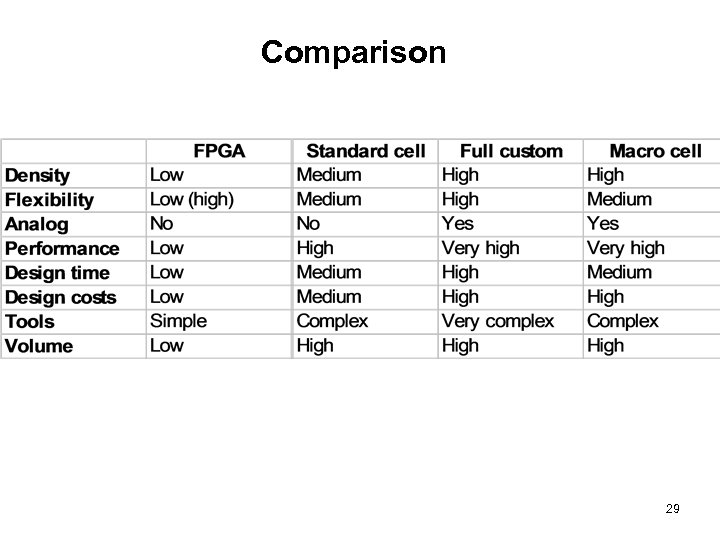
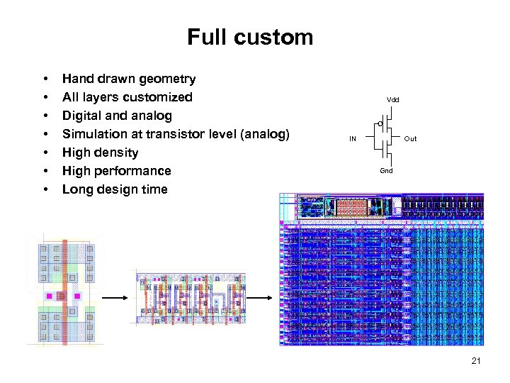 Full custom • • Hand drawn geometry All layers customized Digital and analog Simulation at transistor level (analog) High density High performance Long design time Vdd IN Out Gnd 21
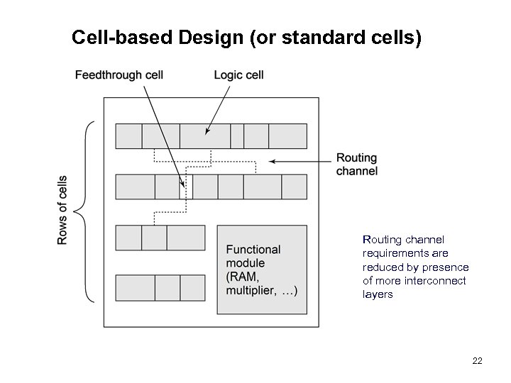 Cell-based Design (or standard cells) Routing channel requirements are reduced by presence of more interconnect layers 22
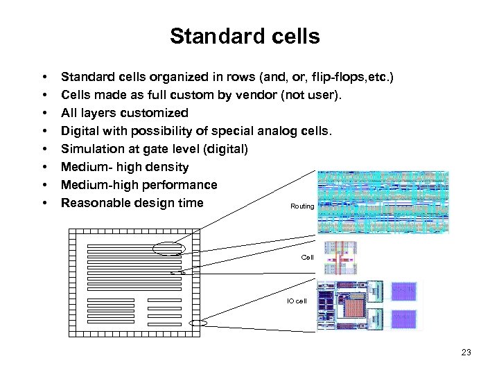 Standard cells • • Standard cells organized in rows (and, or, flip-flops, etc. ) Cells made as full custom by vendor (not user). All layers customized Digital with possibility of special analog cells. Simulation at gate level (digital) Medium- high density Medium-high performance Reasonable design time Routing Cell IO cell 23
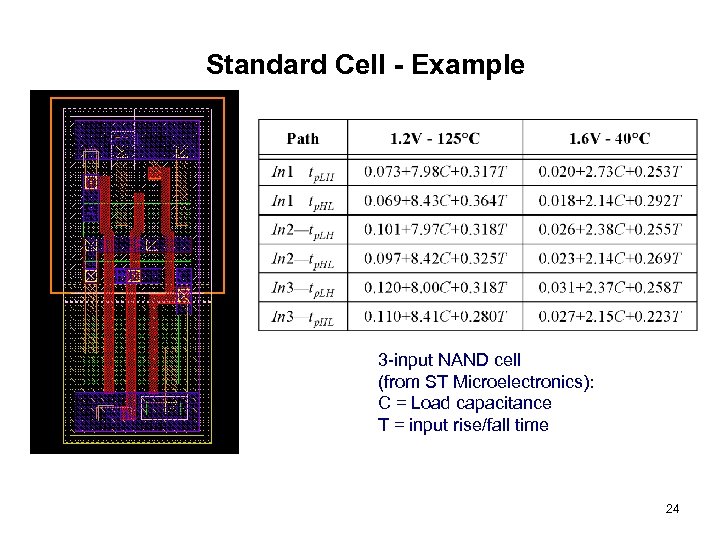 Standard Cell - Example 3 -input NAND cell (from ST Microelectronics): C = Load capacitance T = input rise/fall time 24
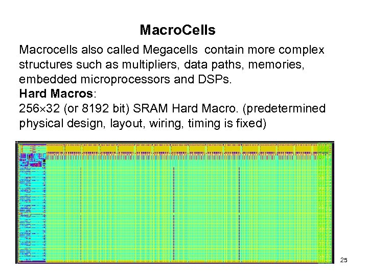 Macro. Cells Macrocells also called Megacells contain more complex structures such as multipliers, data paths, memories, embedded microprocessors and DSPs. Hard Macros: 256 32 (or 8192 bit) SRAM Hard Macro. (predetermined physical design, layout, wiring, timing is fixed) 25
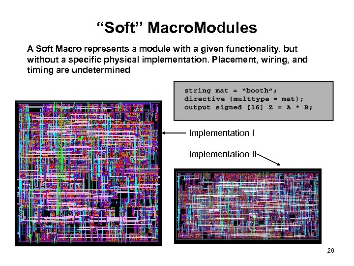 “Soft” Macro. Modules A Soft Macro represents a module with a given functionality, but without a specific physical implementation. Placement, wiring, and timing are undetermined Implementation II 26
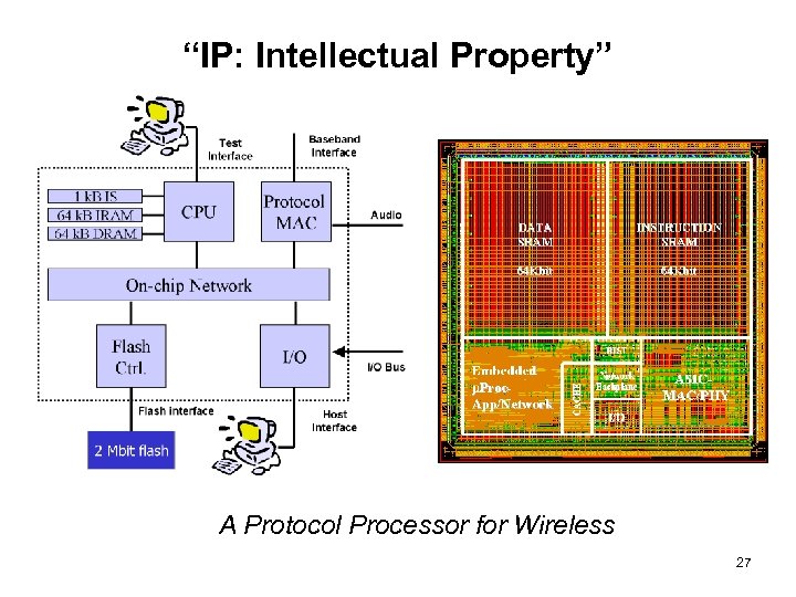 “IP: Intellectual Property” A Protocol Processor for Wireless 27
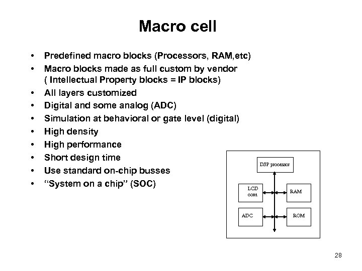 Macro cell • • • Predefined macro blocks (Processors, RAM, etc) Macro blocks made as full custom by vendor ( Intellectual Property blocks = IP blocks) All layers customized Digital and some analog (ADC) Simulation at behavioral or gate level (digital) High density High performance Short design time DSP processor Use standard on-chip busses “System on a chip” (SOC) LCD cont. ADC RAM ROM 28
 Comparison 29
 Semicustom Design Flow Design Iteration Design Capture Pre-Layout Simulation Behavioral HDL Logic Synthesis Structural Floorplanning Post-Layout Simulation Placement Circuit Extraction Routing Physical Tape-out: a binary file is generated containing all the information needed to generate masks for Silicon/ASIC foundry. 30
 Integrating Synthesis with Physical Design RTL in Verilog (Timing) Constraints Physical Synthesis Macromodules Fixed netlists Netlist with Place-and-Route Info Place-and-Route Optimization Artwork 31
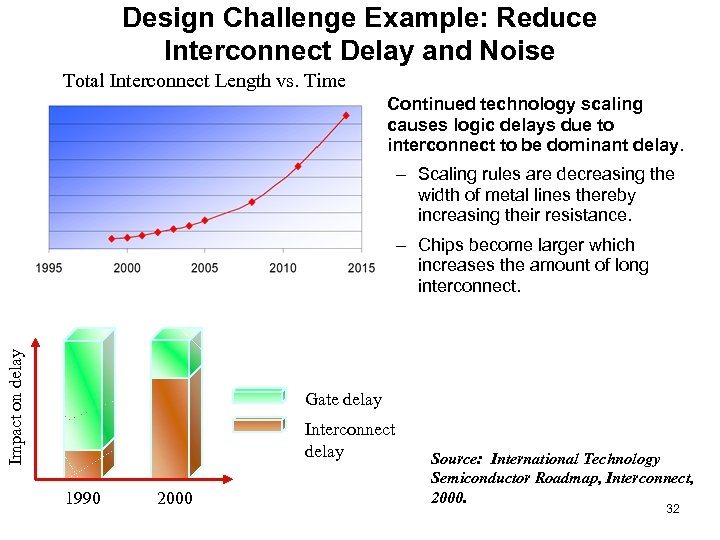 Design Challenge Example: Reduce Interconnect Delay and Noise Total Interconnect Length vs. Time • Continued technology scaling causes logic delays due to interconnect to be dominant delay. – Scaling rules are decreasing the width of metal lines thereby increasing their resistance. Impact on delay – Chips become larger which increases the amount of long interconnect. Gate delay Interconnect delay 1990 2000 Source: International Technology Semiconductor Roadmap, Interconnect, 2000. 32
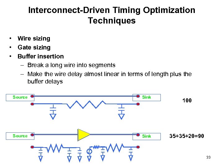 Interconnect-Driven Timing Optimization Techniques • Wire sizing • Gate sizing • Buffer insertion – Break a long wire into segments – Make the wire delay almost linear in terms of length plus the buffer delays Source Sink 100 35+35+20=90 33
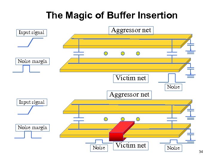 The Magic of Buffer Insertion Aggressor net Input signal Noise margin Victim net Noise Aggressor net Input signal Noise margin Noise Victim net Noise 34
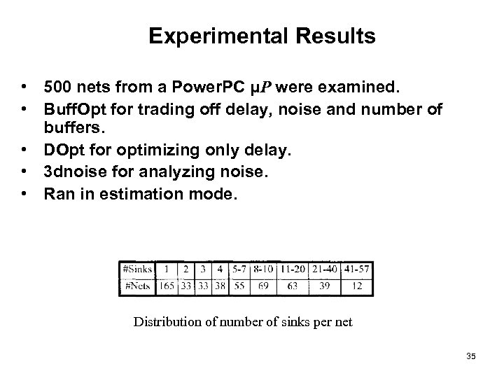 Experimental Results • 500 nets from a Power. PC μP were examined. • Buff. Opt for trading off delay, noise and number of buffers. • DOpt for optimizing only delay. • 3 dnoise for analyzing noise. • Ran in estimation mode. Distribution of number of sinks per net 35
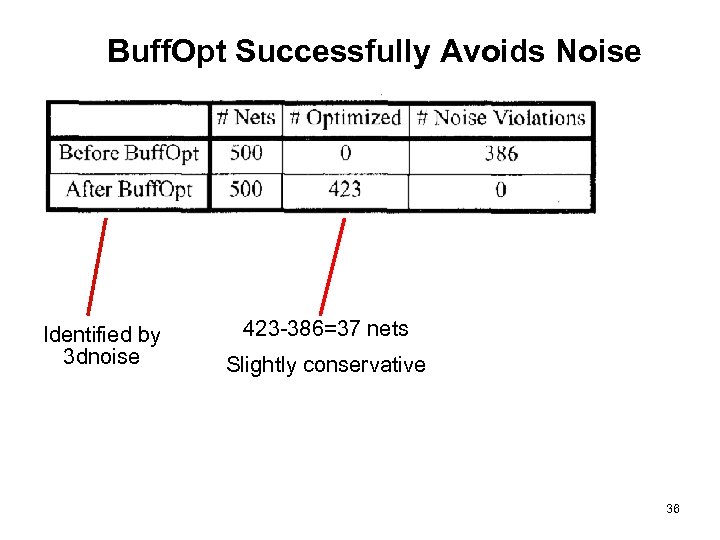 Buff. Opt Successfully Avoids Noise Identified by 3 dnoise 423 -386=37 nets Slightly conservative 36
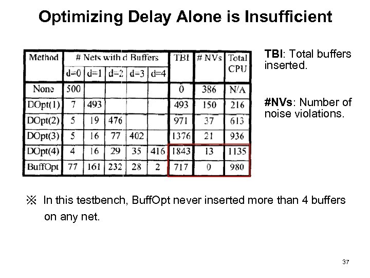 Optimizing Delay Alone is Insufficient TBI: Total buffers inserted. #NVs: Number of noise violations. ※ In this testbench, Buff. Opt never inserted more than 4 buffers on any net. 37
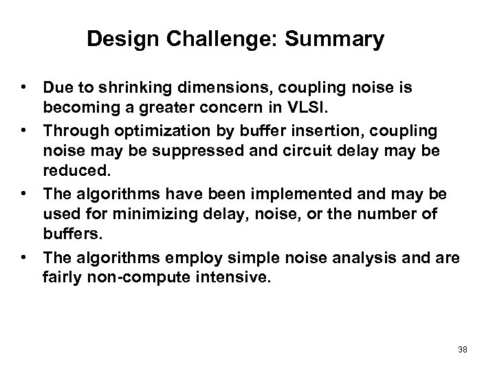 Design Challenge: Summary • Due to shrinking dimensions, coupling noise is becoming a greater concern in VLSI. • Through optimization by buffer insertion, coupling noise may be suppressed and circuit delay may be reduced. • The algorithms have been implemented and may be used for minimizing delay, noise, or the number of buffers. • The algorithms employ simple noise analysis and are fairly non-compute intensive. 38
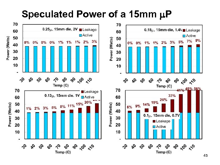
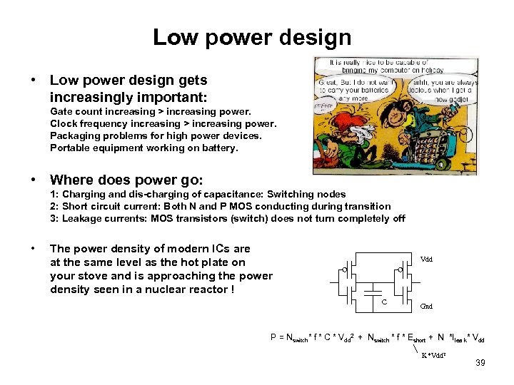 Low power design • Low power design gets increasingly important: Gate count increasing > increasing power. Clock frequency increasing > increasing power. Packaging problems for high power devices. Portable equipment working on battery. • Where does power go: 1: Charging and dis-charging of capacitance: Switching nodes 2: Short circuit current: Both N and P MOS conducting during transition 3: Leakage currents: MOS transistors (switch) does not turn completely off • The power density of modern ICs are at the same level as the hot plate on your stove and is approaching the power density seen in a nuclear reactor ! Vdd C Gnd P = Nswitch* f * C * Vdd 2 + Nswitch * f * Eshort + N *Ilea k* Vdd K*Vdd 2 39
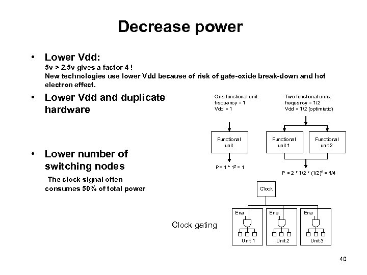 Decrease power • Lower Vdd: 5 v > 2. 5 v gives a factor 4 ! New technologies use lower Vdd because of risk of gate-oxide break-down and hot electron effect. • Lower Vdd and duplicate hardware • Lower number of switching nodes One functional unit: frequency = 1 Vdd = 1 Functional unit Two functional units: frequency = 1/2 Vdd = 1/2 (optimistic) Functional unit 1 P= 1 * 12 = 1 The clock signal often consumes 50% of total power Functional unit 2 P = 2 * 1/2 * (1/2)2 = 1/4 Clock Ena Ena Clock gating Unit 1 Unit 2 Unit 3 40
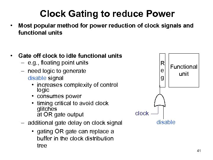 Clock Gating to reduce Power • Most popular method for power reduction of clock signals and functional units • Gate off clock to idle functional units – e. g. , floating point units R Functional e – need logic to generate unit g disable signal • increases complexity of control logic • consumes power • timing critical to avoid clock glitches clock at OR gate output disable – additional gate delay on clock signal • gating OR gate can replace a buffer in the clock distribution tree 41
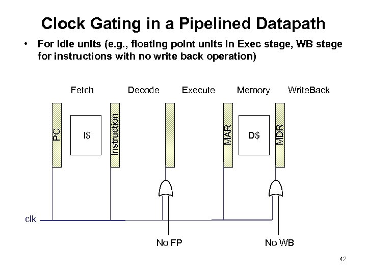 Clock Gating in a Pipelined Datapath • For idle units (e. g. , floating point units in Exec stage, WB stage for instructions with no write back operation) Memory D$ Write. Back MDR Execute MAR I$ Decode Instruction PC Fetch clk No FP No WB 42
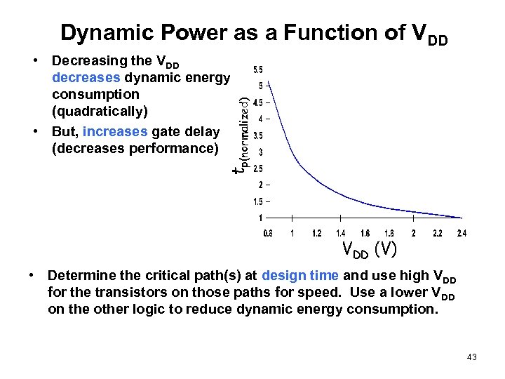 Dynamic Power as a Function of VDD tp(normalized) • Decreasing the VDD decreases dynamic energy consumption (quadratically) • But, increases gate delay (decreases performance) VDD (V) • Determine the critical path(s) at design time and use high VDD for the transistors on those paths for speed. Use a lower VDD on the other logic to reduce dynamic energy consumption. 43
 Dynamic Frequency and Voltage Scaling • Intel’s Speed. Step – Hardware that steps down the clock frequency (dynamic frequency scaling – DFS) when the user unplugs from AC power • PLL from 650 MHz 500 MHz – CPU stalls during Speed. Step adjustment • Transmeta Long. Run – Hardware that applies both DFS and DVS (dynamic supply voltage scaling) • 32 levels of VDD from 1. 1 V to 1. 6 V • PLL from 200 MHz 700 MHz in increments of 33 MHz – Triggered when CPU load change is detected by software • heavier load ramp up VDD, when stable speed up clock • lighter load slow down clock, when PLL locks onto new rate, ramp down VDD – CPU stalls only during PLL relock (< 20 microsec) 44
 Speculated Power of a 15 mm m. P 45
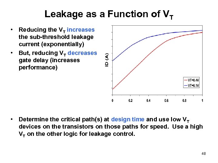 Leakage as a Function of VT • Reducing the VT increases the sub-threshold leakage current (exponentially) • But, reducing VT decreases gate delay (increases performance) • Determine the critical path(s) at design time and use low VT devices on the transistors on those paths for speed. Use a high VT on the other logic for leakage control. 46
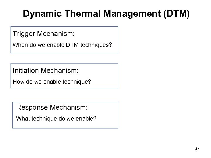 Dynamic Thermal Management (DTM) Trigger Mechanism: When do we enable DTM techniques? Initiation Mechanism: How do we enable technique? Response Mechanism: What technique do we enable? 47
 DTM Trigger Mechanisms • Mechanism: How to deduce temperature? • Direct approach: on-chip temperature sensors – Based on differential voltage change across 2 diodes of different sizes – May require >1 sensor – Hysteresis and delay are problems • Policy: When to begin responding? – Trigger level set too high means higher packaging costs – Trigger level set too low means frequent triggering and loss in performance • Choose trigger level to exploit difference between average and worst case power 48
 DTM Initiation and Response Mechanisms • Operating system or microarchitectural control? – Hardware support can reduce performance penalty by 20 -30% • Initiation of policy incurs some delay – When using DVS and/or DFS, much of the performance penalty can be attributed to enabling/disabling overhead – Increasing policy delay reduces overhead; smarter initiation techniques would help as well • Thermal window (100 Kcycles+) – Larger thermal windows “smooth” short thermal spikes 49
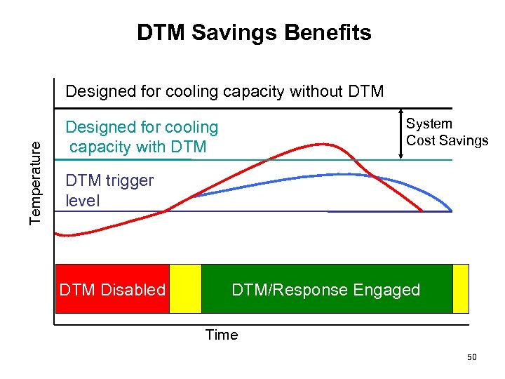 DTM Savings Benefits Temperature Designed for cooling capacity without DTM System Cost Savings Designed for cooling capacity with DTM trigger level DTM Disabled DTM/Response Engaged Time 50
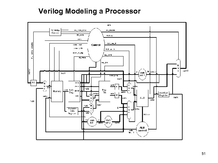 Verilog Modeling a Processor 51
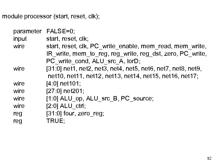 module processor (start, reset, clk); parameter FALSE=0; input start, reset, clk; wire start, reset, clk, PC_write_enable, mem_read, mem_write, IR_write, mem_to_reg, reg_write, reg_dst, zero, PC_write_cond, ALU_src_A, Ior. D; wire [31: 0] net 1, net 2, net 3, net 4, net 5, net 6, net 7, net 8, net 9, net 10, net 11, net 12, net 13, net 14, net 15, net 16, net 17; wire [4: 0] net 101; wire [27: 0] net 201; wire [1: 0] ALU_op, ALU_src_B, PC_source; wire [2: 0] ALU_ctrl; reg [31: 0] four, zero_reg; reg TRUE; 52
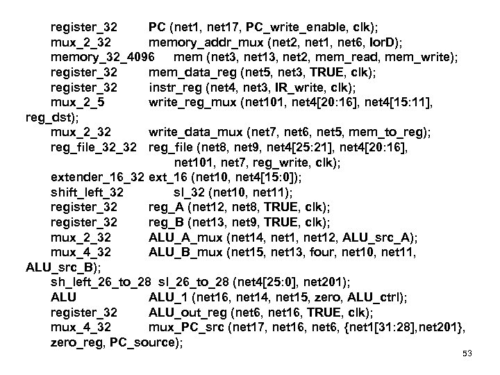 register_32 PC (net 1, net 17, PC_write_enable, clk); mux_2_32 memory_addr_mux (net 2, net 1, net 6, Ior. D); memory_32_4096 mem (net 3, net 13, net 2, mem_read, mem_write); register_32 mem_data_reg (net 5, net 3, TRUE, clk); register_32 instr_reg (net 4, net 3, IR_write, clk); mux_2_5 write_reg_mux (net 101, net 4[20: 16], net 4[15: 11], reg_dst); mux_2_32 write_data_mux (net 7, net 6, net 5, mem_to_reg); reg_file_32_32 reg_file (net 8, net 9, net 4[25: 21], net 4[20: 16], net 101, net 7, reg_write, clk); extender_16_32 ext_16 (net 10, net 4[15: 0]); shift_left_32 sl_32 (net 10, net 11); register_32 reg_A (net 12, net 8, TRUE, clk); register_32 reg_B (net 13, net 9, TRUE, clk); mux_2_32 ALU_A_mux (net 14, net 12, ALU_src_A); mux_4_32 ALU_B_mux (net 15, net 13, four, net 10, net 11, ALU_src_B); sh_left_26_to_28 sl_26_to_28 (net 4[25: 0], net 201); ALU_1 (net 16, net 14, net 15, zero, ALU_ctrl); register_32 ALU_out_reg (net 6, net 16, TRUE, clk); mux_4_32 mux_PC_src (net 17, net 16, net 6, {net 1[31: 28], net 201}, zero_reg, PC_source); 53
![ALU_control ALU_cont (ALU_ctrl, ALU_op, net 4[5: 0], TRUE); PC_write_ctrl PC_ctrl (PC_write_enable, PC_write, PC_write_cond, zero); ALU_control ALU_cont (ALU_ctrl, ALU_op, net 4[5: 0], TRUE); PC_write_ctrl PC_ctrl (PC_write_enable, PC_write, PC_write_cond, zero);](https://present5.com/presentation/2384f1e941d6bc34763b82cfd739a982/image-54.jpg) ALU_control ALU_cont (ALU_ctrl, ALU_op, net 4[5: 0], TRUE); PC_write_ctrl PC_ctrl (PC_write_enable, PC_write, PC_write_cond, zero); control_unit ctrl (start, reset, clk, mem_read, mem_write, IR_write, mem_to_reg, reg_write, reg_dst, Ior. D, PC_write, PC_write_cond, ALU_src_A, ALU_src_B, ALU_op, PC_source, net 4[31: 26]); initial begin four = 4; zero_reg = 0; TRUE = 1; endmodule 54
ALU_control ALU_cont (ALU_ctrl, ALU_op, net 4[5: 0], TRUE); PC_write_ctrl PC_ctrl (PC_write_enable, PC_write, PC_write_cond, zero); control_unit ctrl (start, reset, clk, mem_read, mem_write, IR_write, mem_to_reg, reg_write, reg_dst, Ior. D, PC_write, PC_write_cond, ALU_src_A, ALU_src_B, ALU_op, PC_source, net 4[31: 26]); initial begin four = 4; zero_reg = 0; TRUE = 1; endmodule 54


