ecae823ceb11eab68aac6c9a9dca82a1.ppt
- Количество слайдов: 38
 VLSI Signal Processing Dr. Elwin Chandra Monie Department of ECE, RMK Engineering College
 VL 7101 VLSI SIGNAL PROCESSING OBJECTIVES To understand the various VLSI architectures for digital signal processing. To know the techniques of critical path and algorithmic strength reduction in the filter structures. To study the performance parameters, viz. area, speed and power. OUTCOMES To be able to design architectures for DSP algorithms. To be able to optimize design in terms of area, speed and power. To be able to incorporate pipeline based architectures in the design. To be able to carry out HDL simulation of various DSP algorithms. 3 Dept. of ECE, RMK Engineering College
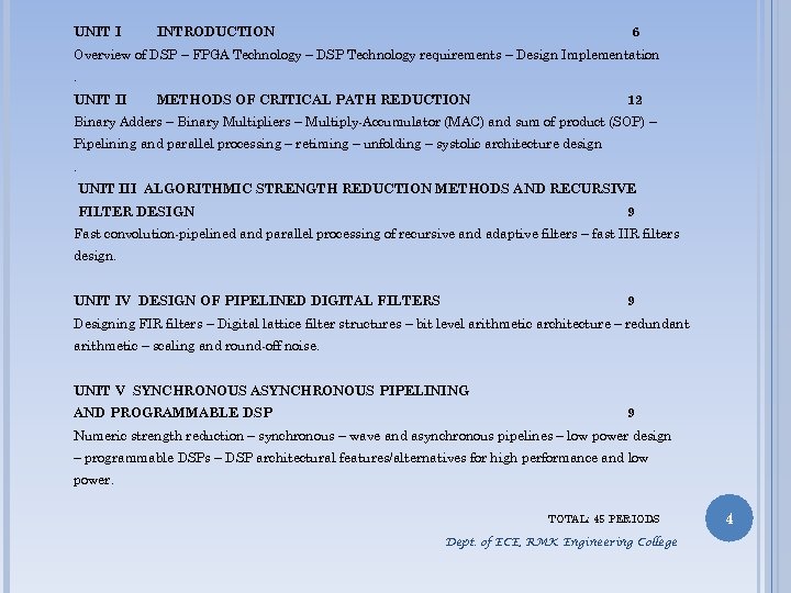 UNIT I INTRODUCTION 6 Overview of DSP – FPGA Technology – DSP Technology requirements – Design Implementation. UNIT II METHODS OF CRITICAL PATH REDUCTION 12 Binary Adders – Binary Multipliers – Multiply-Accumulator (MAC) and sum of product (SOP) – Pipelining and parallel processing – retiming – unfolding – systolic architecture design. UNIT III ALGORITHMIC STRENGTH REDUCTION METHODS AND RECURSIVE FILTER DESIGN 9 Fast convolution-pipelined and parallel processing of recursive and adaptive filters – fast IIR filters design. UNIT IV DESIGN OF PIPELINED DIGITAL FILTERS 9 Designing FIR filters – Digital lattice filter structures – bit level arithmetic architecture – redundant arithmetic – scaling and round-off noise. UNIT V SYNCHRONOUS ASYNCHRONOUS PIPELINING AND PROGRAMMABLE DSP 9 Numeric strength reduction – synchronous – wave and asynchronous pipelines – low power design – programmable DSPs – DSP architectural features/alternatives for high performance and low power. TOTAL: 45 PERIODS Dept. of ECE, RMK Engineering College 4
 REFERENCES: 1. Keshab K. Parhi, “VLSI Digital Signal Processing Systems, Design and Implementation”, John Wiley, Indian Reprint, 2007. 2. U. Meyer – Baese, "Digital Signal Processing with Field Programmable Arrays", Springer, Second Edition, Indian Reprint, 2007. 3. S. Y. Kuang, H. J. White house, T. Kailath, “VLSI and Modern Signal Processing”, Prentice Hall, 1995. 5 Dept. of ECE, RMK Engineering College
 APPLICATIONS 6 Dept. of ECE, R M K Engineering College
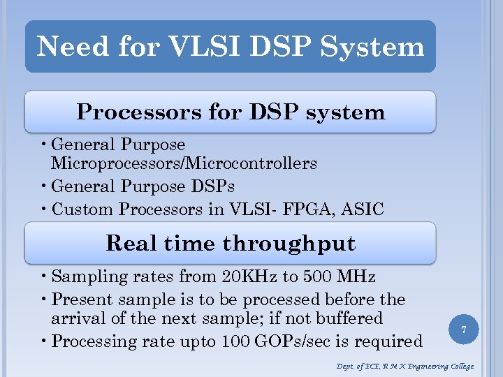 Need for VLSI DSP System Processors for DSP system • General Purpose Microprocessors/Microcontrollers • General Purpose DSPs • Custom Processors in VLSI- FPGA, ASIC Real time throughput • Sampling rates from 20 KHz to 500 MHz • Present sample is to be processed before the arrival of the next sample; if not buffered • Processing rate upto 100 GOPs/sec is required 7 Dept. of ECE, R M K Engineering College
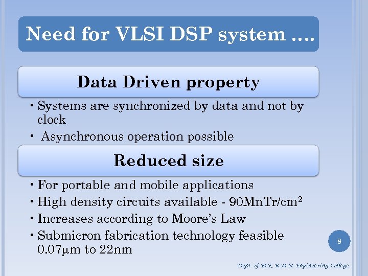 Need for VLSI DSP system …. Data Driven property • Systems are synchronized by data and not by clock • Asynchronous operation possible Reduced size • For portable and mobile applications • High density circuits available - 90 Mn. Tr/cm 2 • Increases according to Moore’s Law • Submicron fabrication technology feasible 0. 07µm to 22 nm 8 Dept. of ECE, R M K Engineering College
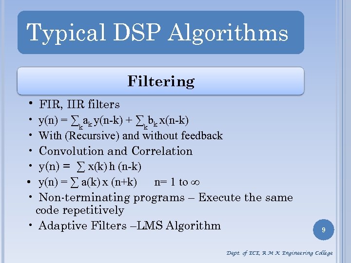 Typical DSP Algorithms Filtering • FIR, IIR filters • • • y(n) = ∑ ak y(n-k) + ∑ bk x(n-k) k k With (Recursive) and without feedback Convolution and Correlation y(n) = ∑ x(k) h (n-k) y(n) = ∑ a(k) x (n+k) n= 1 to ∞ Non-terminating programs – Execute the same code repetitively • Adaptive Filters –LMS Algorithm 9 Dept. of ECE, R M K Engineering College
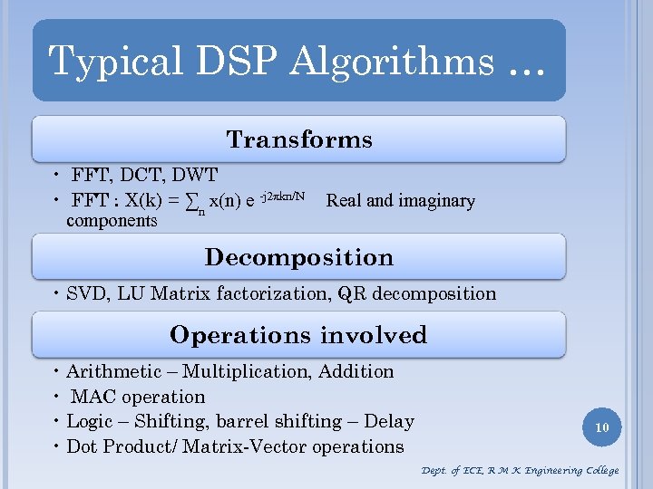 Typical DSP Algorithms … Transforms • FFT, DCT, DWT • FFT : X(k) = ∑n x(n) e -j 2πkn/N components Real and imaginary Decomposition • SVD, LU Matrix factorization, QR decomposition Operations involved • Arithmetic – Multiplication, Addition • MAC operation • Logic – Shifting, barrel shifting – Delay • Dot Product/ Matrix-Vector operations 10 Dept. of ECE, R M K Engineering College
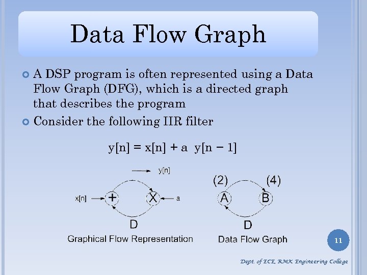 Data Flow Graph A DSP program is often represented using a Data Flow Graph (DFG), which is a directed graph that describes the program Consider the following IIR filter y[n] = x[n] + a y[n − 1] 11 Dept. of ECE, RMK Engineering College
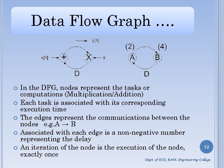 Data Flow Graph …. In the DFG, nodes represent the tasks or computations (Multiplication/Addition) Each task is associated with its corresponding execution time The edges represent the communications between the nodes e. g. A → B Associated with each edge is a non-negative number representing the delay An iteration of the node is the execution of the node, exactly once 12 Dept. of ECE, RMK Engineering College
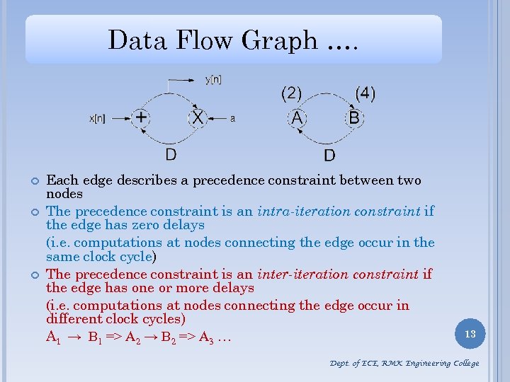 Data Flow Graph …. Each edge describes a precedence constraint between two nodes The precedence constraint is an intra-iteration constraint if the edge has zero delays (i. e. computations at nodes connecting the edge occur in the same clock cycle) The precedence constraint is an inter-iteration constraint if the edge has one or more delays (i. e. computations at nodes connecting the edge occur in different clock cycles) A 1 → B 1 => A 2 → B 2 => A 3 … 13 Dept. of ECE, RMK Engineering College
 Speed – Highest frequency of operation Area – minimum area required Power – minimum power to operate All three may not be satisfied simultaneously 14 Dept. of ECE, RMK Engineering College
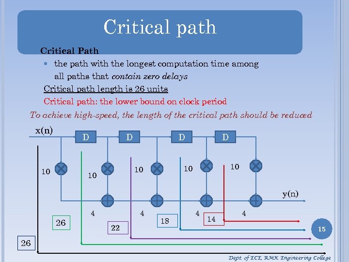 Critical path Critical Path the path with the longest computation time among all paths that contain zero delays Critical path length is 26 units Critical path: the lower bound on clock period To achieve high-speed, the length of the critical path should be reduced x(n) D 10 D D 10 10 D y(n) 26 4 4 22 18 4 14 4 15 26 Dept. of ECE, RMK Engineering College
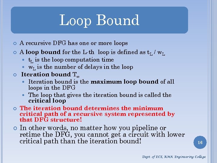 Loop Bound A recursive DFG has one or more loops A loop bound for the L-th loop is defined as t. L / w. L t. L is the loop computation time w. L is the number of delays in the loop Iteration bound T∞ Iteration bound is the maximum loop bound of all loops in the DFG The loop that gives the iteration bound is called the critical loop The iteration bound determines the minimum critical path of a recursive system represented by that DFG structure! In other words, no matter how you pipeline or retime the DFG, you cannot get a circuit with lower critical path than the iteration bound! 16 Dept. of ECE, RMK Engineering College
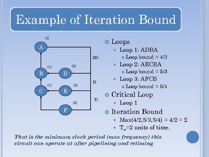 Example of Iteration Bound (1) A Loops 2 D B D (1) C (2) (1) D Loop bound = 5/4 Critical Loop bound = 5/3 Loop 3: AFCB E (2) D Loop bound = 4/2 Loop 2: AECBA (2) F Loop 1: ADBA Loop 1 Iteration Bound Max{4/2, 5/3, 5/4} = 4/2 = 2 T∞=2 units of time. That is the minimum clock period (max frequency) this circuit can operate at after pipelining and retiming
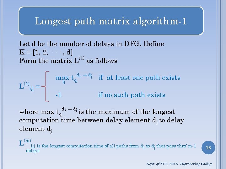 Longest path matrix algorithm-1 Let d be the number of delays in DFG. Define K = [1, 2, · · · , d] Form the matrix L(1) as follows L(1)i, j = max tqd i → dj if at least one path exists q -1 if no such path exists where max tqd i → dj is the maximum of the longest computation time between delay element di to delay element dj L(m)i, j is the longest computation time of all paths from di to dj that pass thro’ m-1 delays 18 Dept. of ECE, RMK Engineering College
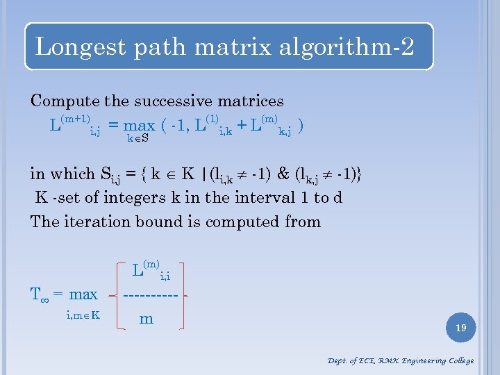 Longest path matrix algorithm-2 Compute the successive matrices L(m+1)i, j = max ( -1, L(1)i, k + L(m)k, j ) k S in which Si, j = { k K |(li, k -1) & (lk, j -1)} K -set of integers k in the interval 1 to d The iteration bound is computed from T∞ = max i, m K L(m)i, i -----m 19 Dept. of ECE, RMK Engineering College
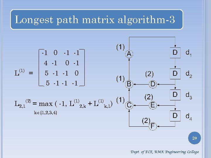 Longest path matrix algorithm-3 L(1) = -1 0 -1 -1 4 -1 0 -1 5 -1 -1 0 5 -1 -1 -1 L 2, 1(2) = max ( -1, L(1)2, k + L(1)k, 1) k {1, 2, 3, 4} 20 Dept. of ECE, RMK Engineering College
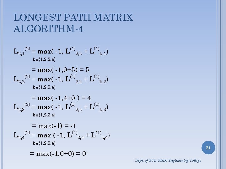 LONGEST PATH MATRIX ALGORITHM-4 L 2, 1(2) = max( -1, L(1)2, k + L(1)k, 1) k {1, 2, 3, 4} = max( -1, 0+5) = 5 L 2, 2(2) = max( -1, L(1)2, k + L(1)k, 2) k {1, 2, 3, 4} = max( -1, 4+0 ) = 4 L 2, 3(2) = max( -1, L(1)2, k + L(1)k, 3) k {1, 2, 3, 4} = max(-1) = -1 L 2, 4(2) = max ( -1, L(1)2, 4 + L(1)k, 4) k {1, 2, 3, 4} 21 = max(-1, 0+0) = 0 Dept. of ECE, RMK Engineering College
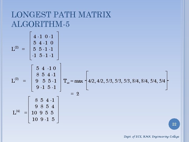 LONGEST PATH MATRIX ALGORITHM-5 L(2) = L(3) = 4 -1 0 -1 5 4 -1 0 5 5 -1 -1 -1 5 4 8 5 9 -1 -1 0 4 -1 5 -1 T∞ = max 4/2, 5/3, 8/4, 5/4 = 2 L(4) 8 9 = 10 10 5 4 -1 8 5 4 9 5 5 9 -1 5 22 Dept. of ECE, RMK Engineering College
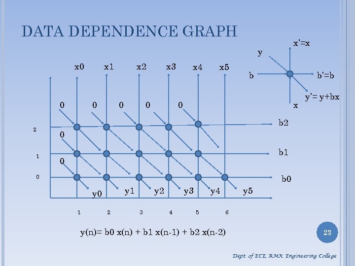 DATA DEPENDENCE GRAPH x’=x y x 0 0 2 1 x 1 0 x 2 0 x 3 0 x 4 x 5 b b’=b 0 x y’= y+bx b 2 0 b 1 0 b 0 0 y 1 y 0 1 2 y 2 3 y 3 4 y 4 5 y 5 6 y(n)= b 0 x(n) + b 1 x(n-1) + b 2 x(n-2) 23 Dept. of ECE, RMK Engineering College
 PIPELINING IN FIR FILTERS Reduce the critical path Increase the clock speed or sample speed Reduce power consumption Introduce pipelining latches along the data path 24 Dept. of ECE, RMK Engineering College
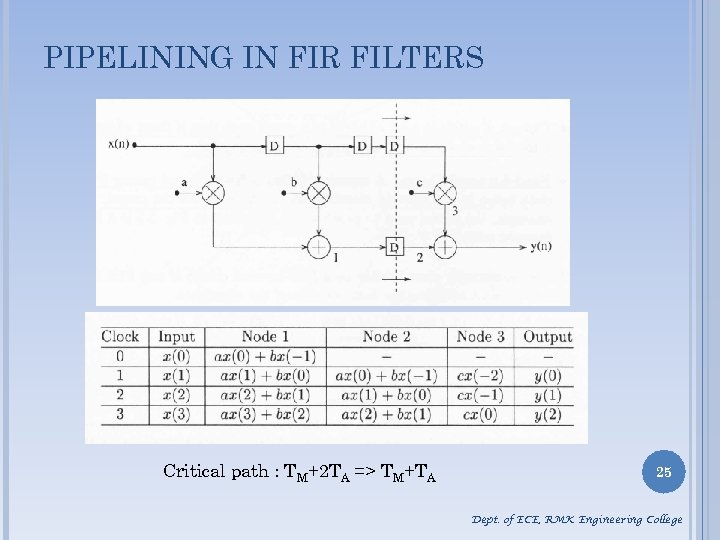 PIPELINING IN FIR FILTERS Critical path : TM+2 TA => TM+TA 25 Dept. of ECE, RMK Engineering College
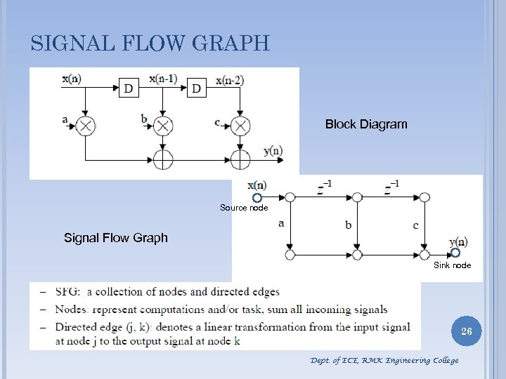 SIGNAL FLOW GRAPH Block Diagram Source node Signal Flow Graph Sink node 26 Dept. of ECE, RMK Engineering College
 GENERAL METHOD OF PIPELINING Pipelining latches can only be placed across any feedforward cutset of the graph without affecting of the structure Cutset: A cutset is a set of edges of a graph such that if these edges are removed from the graph, the graph becomes disjoint. Feed-forward cutset: A cutset is called a feedforward cutset if the data move in the forward direction on all the edges of the cutset Limitations of Pipelining Increase in Latency : The difference in the availability of the first output in the pipelined and the sequential system Increase in the number of latches 27 Dept. of ECE, RMK Engineering College
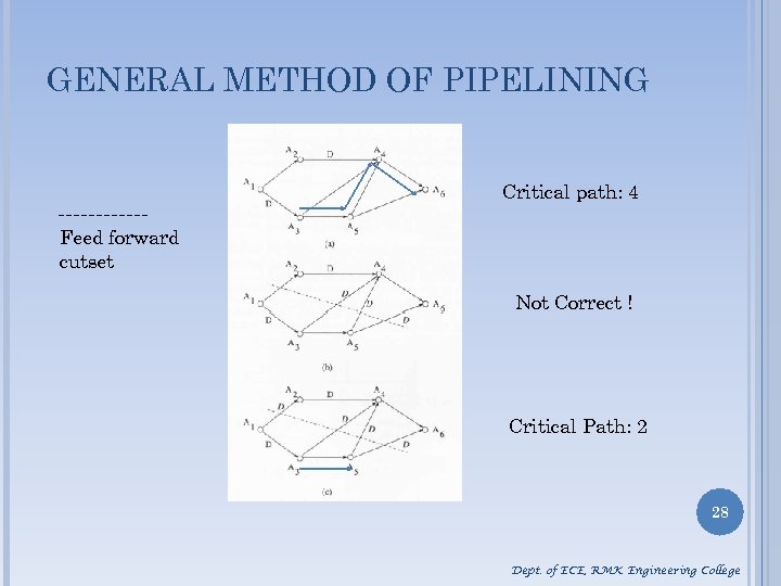 GENERAL METHOD OF PIPELINING Critical path: 4 Feed forward cutset Not Correct ! Critical Path: 2 28 Dept. of ECE, RMK Engineering College
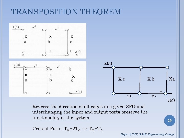 TRANSPOSITION THEOREM x x x + + x(n) + x x Xc Xb + Z-1 Reverse the direction of all edges in a given SFG and interchanging the input and output ports preserve the functionality of the system Xa + Z-1 y(n) 29 Critical Path : TM+2 TA => TM+TA Dept. of ECE, RMK Engineering College
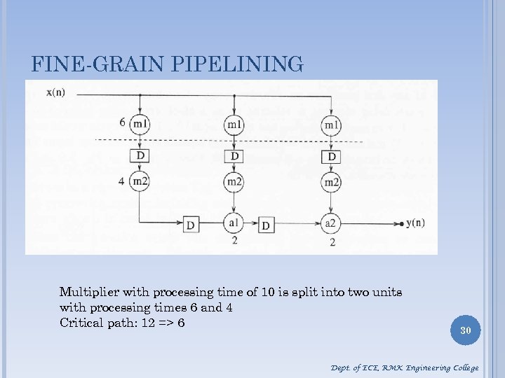 FINE-GRAIN PIPELINING Multiplier with processing time of 10 is split into two units with processing times 6 and 4 Critical path: 12 => 6 30 Dept. of ECE, RMK Engineering College
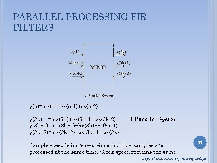 PARALLEL PROCESSING FIR FILTERS y(n)= ax(n)+bx(n-1)+cx(n-2) y(3 k) = ax(3 k)+bx(3 k-1)+cx(3 k-2) y(3 k+1)= ax(3 k+1)+bx(3 k)+cx(3 k-1) y(3 k+2)= ax(3 k+2)+bx(3 k+1)+cx(3 k) 3 -Parallel System Sample speed is increased since multiple samples are processed at the same time. Clock speed remains the same 31 Dept. of ECE, RMK Engineering College
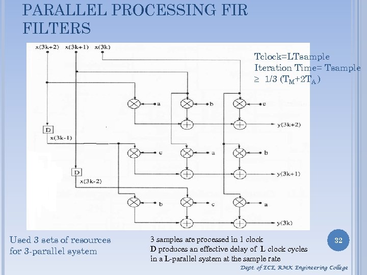 PARALLEL PROCESSING FIR FILTERS Tclock=LTsample Iteration Time= Tsample 1/3 (TM+2 TA ) Used 3 sets of resources for 3 -parallel system 3 samples are processed in 1 clock D produces an effective delay of L clock cycles in a L-parallel system at the sample rate 32 Dept. of ECE, RMK Engineering College
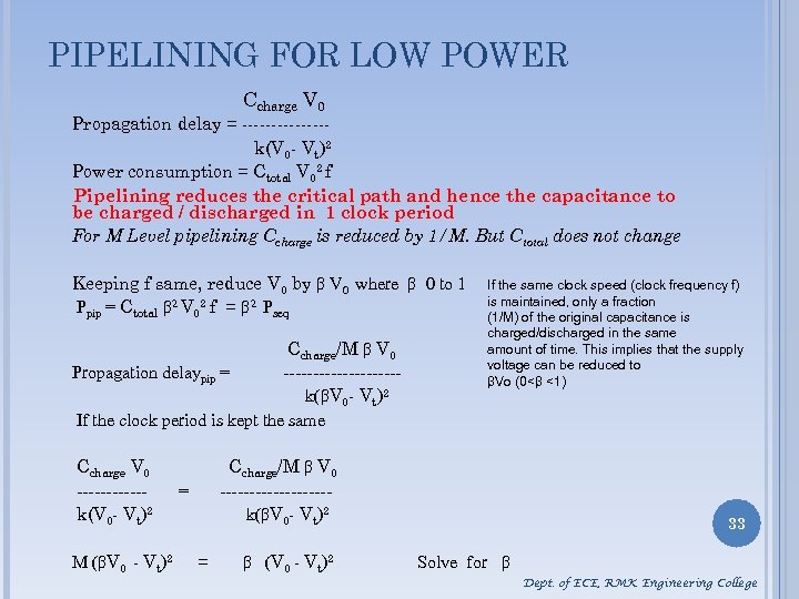 PIPELINING FOR LOW POWER Ccharge V 0 Propagation delay = -------k(V 0 - Vt)2 Power consumption = Ctotal V 02 f Pipelining reduces the critical path and hence the capacitance to be charged / discharged in 1 clock period For M Level pipelining Ccharge is reduced by 1/M. But Ctotal does not change Keeping f same, reduce V 0 by β V 0 where β 0 to 1 Ppip = Ctotal β 2 V 02 f = β 2 Pseq Ccharge/M β V 0 Propagation delaypip = ----------k(βV 0 - Vt)2 If the clock period is kept the same Ccharge V 0 ------k(V 0 - Vt)2 M (βV 0 - Vt)2 If the same clock speed (clock frequency f) is maintained, only a fraction (1/M) of the original capacitance is charged/discharged in the same amount of time. This implies that the supply voltage can be reduced to βVo (0<β <1) Ccharge/M β V 0 ---------k(βV 0 - Vt)2 = = β (V 0 - Vt)2 33 Solve for β Dept. of ECE, RMK Engineering College
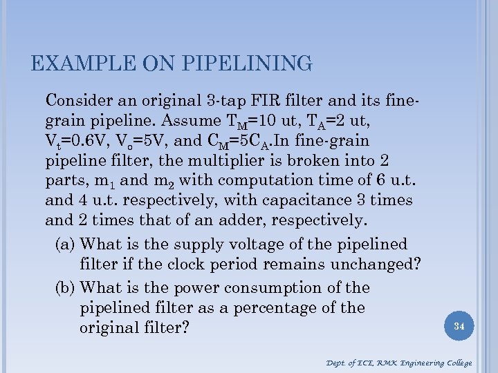 EXAMPLE ON PIPELINING Consider an original 3 -tap FIR filter and its finegrain pipeline. Assume TM=10 ut, TA=2 ut, Vt=0. 6 V, Vo=5 V, and CM=5 CA. In fine-grain pipeline filter, the multiplier is broken into 2 parts, m 1 and m 2 with computation time of 6 u. t. and 4 u. t. respectively, with capacitance 3 times and 2 times that of an adder, respectively. (a) What is the supply voltage of the pipelined filter if the clock period remains unchanged? (b) What is the power consumption of the pipelined filter as a percentage of the original filter? 34 Dept. of ECE, RMK Engineering College
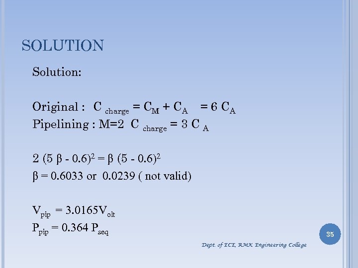 SOLUTION Solution: Original : C charge = CM + CA = 6 CA Pipelining : M=2 C charge = 3 C A 2 (5 β - 0. 6)2 = β (5 - 0. 6)2 β = 0. 6033 or 0. 0239 ( not valid) Vpip = 3. 0165 Volt Ppip = 0. 364 Pseq 35 Dept. of ECE, RMK Engineering College
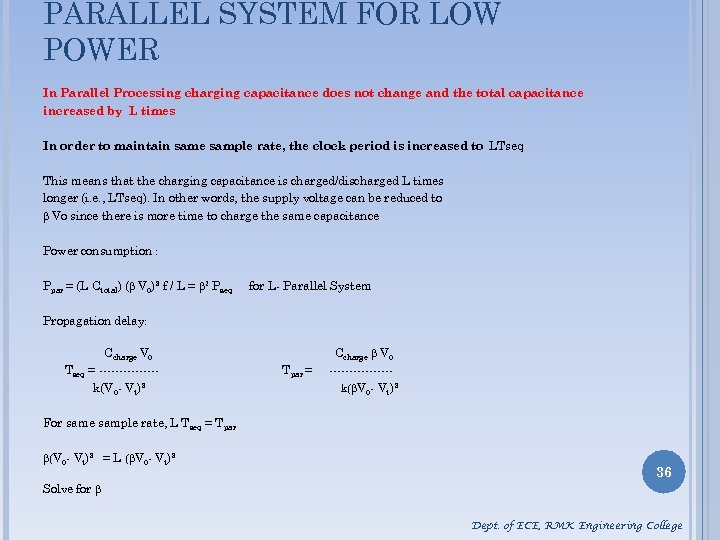 PARALLEL SYSTEM FOR LOW POWER In Parallel Processing charging capacitance does not change and the total capacitance increased by L times In order to maintain same sample rate, the clock period is increased to LTseq This means that the charging capacitance is charged/discharged L times longer (i. e. , LTseq). In other words, the supply voltage can be reduced to β Vo since there is more time to charge the same capacitance Power consumption : Ppar = (L Ctotal) (β V 0)2 f / L = β 2 Pseq for L- Parallel System Propagation delay: Ccharge V 0 Tseq = -------k(V 0 - Vt)2 T par = Ccharge β V 0 --------k(βV 0 - Vt)2 For same sample rate, L Tseq = Tpar β(V 0 - Vt)2 = L (βV 0 - Vt)2 36 Solve for β Dept. of ECE, RMK Engineering College
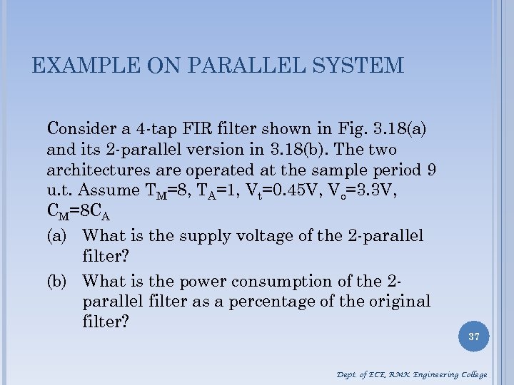 EXAMPLE ON PARALLEL SYSTEM Consider a 4 -tap FIR filter shown in Fig. 3. 18(a) and its 2 -parallel version in 3. 18(b). The two architectures are operated at the sample period 9 u. t. Assume TM=8, TA=1, Vt=0. 45 V, Vo=3. 3 V, CM=8 CA (a) What is the supply voltage of the 2 -parallel filter? (b) What is the power consumption of the 2 parallel filter as a percentage of the original filter? 37 Dept. of ECE, RMK Engineering College
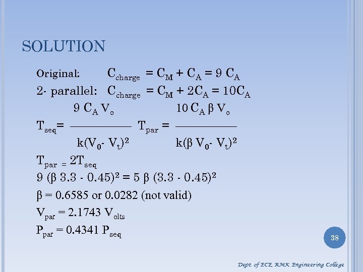 SOLUTION Ccharge = CM + CA = 9 CA 2 - parallel: Ccharge = CM + 2 CA = 10 CA 9 C A Vo 10 CA β Vo Tseq= Tpar = k(V 0 - Vt)2 k(β V 0 - Vt)2 Tpar = 2 Tseq 9 (β 3. 3 - 0. 45)2 = 5 β (3. 3 - 0. 45)2 β = 0. 6585 or 0. 0282 (not valid) Vpar = 2. 1743 Volts Ppar = 0. 4341 Pseq Original: 38 Dept. of ECE, RMK Engineering College
 PROBLEMS & ASSIGNMENTS 1) Prob. 2. 7. 1 (a) 2) Prob. 2. 7. 4 Assignment 1) Design a Low pass filter with sample rate of 48 KHz and order 40 with cut off frequency of 10 KHz. Write VHDL/Verilog code and simulate Hint: Use Matlab to find the coefficients and test the filter functionality by testing the impulse response 2) Implement a 4 -tap filter in direct form and in transpose form. Introduce pipelining and compare the performance 39 Dept. of ECE, RMK Engineering College


