bb1996b9c0f5534636fdc327ff8f068b.ppt
- Количество слайдов: 123
 VLSI Overview Chia-Chun Tsai Professor & Chairman Department of Electronic Engineering National Taipei University of Technology Email: cctsai@ntut. edu. tw Website: www. ntut. edu. tw/~cctsai MIT, June 26, 2003 VLSI Lab 205 / C-C Tsai 1
 Outline VLSI View from Evolution VLSI View from Research VLSI View from Chip Design VLSI View from Industry VLSI View from SOC VLSI View from Education Conclusion VLSI Lab 205 / C-C Tsai 2
 VLSI View from Evolution The First Computer VLSI Lab 205 / C-C Tsai 3
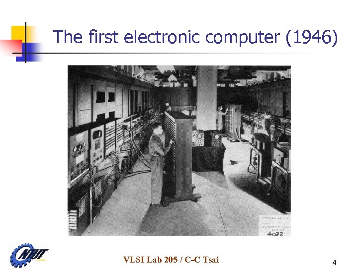 The first electronic computer (1946) VLSI Lab 205 / C-C Tsai 4
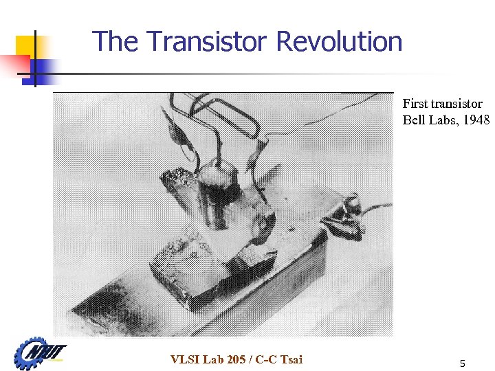 The Transistor Revolution First transistor Bell Labs, 1948 VLSI Lab 205 / C-C Tsai 5
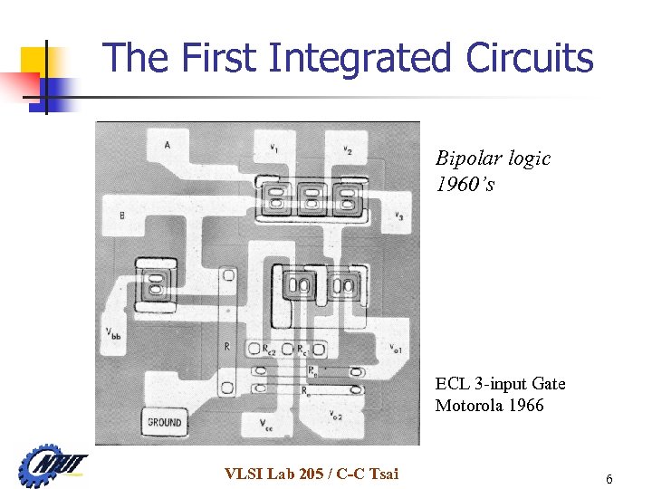 The First Integrated Circuits Bipolar logic 1960’s ECL 3 -input Gate Motorola 1966 VLSI Lab 205 / C-C Tsai 6
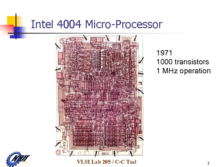 Intel 4004 Micro-Processor 1971 1000 transistors 1 MHz operation VLSI Lab 205 / C-C Tsai 7
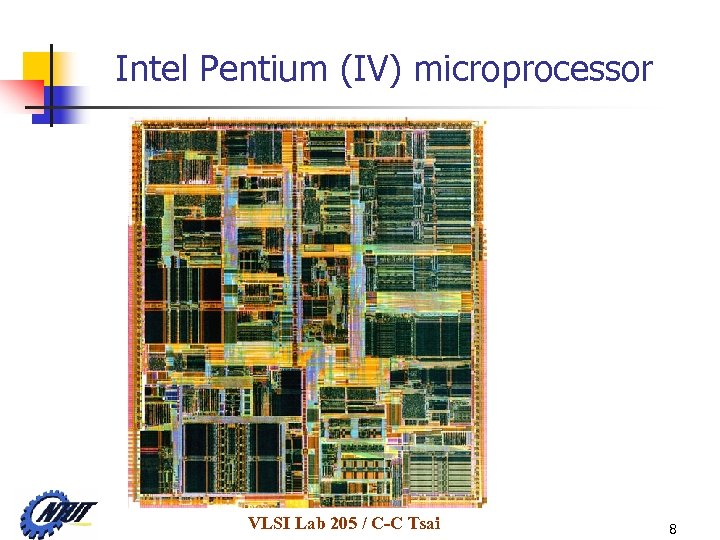 Intel Pentium (IV) microprocessor VLSI Lab 205 / C-C Tsai 8
 Moore’s Law In 1965, Gordon Moore noted that the number of transistors on a chip doubled every 18 to 24 months. He made a prediction that semiconductor technology will double its effectiveness every 18 months VLSI Lab 205 / C-C Tsai 9
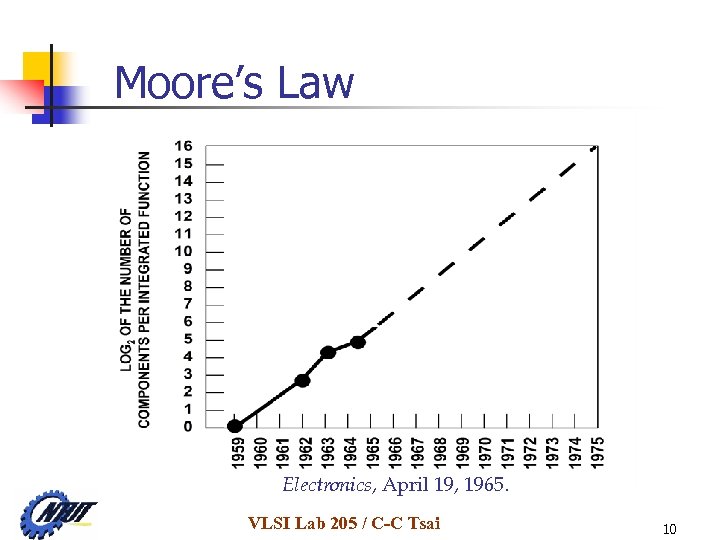 Moore’s Law Electronics, April 19, 1965. VLSI Lab 205 / C-C Tsai 10
 Technology Evolution • ITRS(國際半導體技術籃圖 ) plan: 2004 -> 90 nm (0. 09 um) ,2007 -> 65 nm • TSMC: 2002 Winter->90 nm for CPU and graphic chips 2005 ->65 nm, 35 nm developed in Lab • Intel : 2003 Spring->90 nm for CPU Pentium 4 • Copper process: VLSI Lab 205 / C-C Tsai 11
 Technology Evolution Human hair’s diameter: 70~100 um Human felling cell: 50~100 um Human ovum cell: 100 um Plant cell: 100 um Human red hemocyte: 5 um Germ: 1~8 um Virus:hundreds nm Protein:number tens nm DNA: 2 nm Atom: 0. 1 nm VLSI Lab 205 / C-C Tsai 12
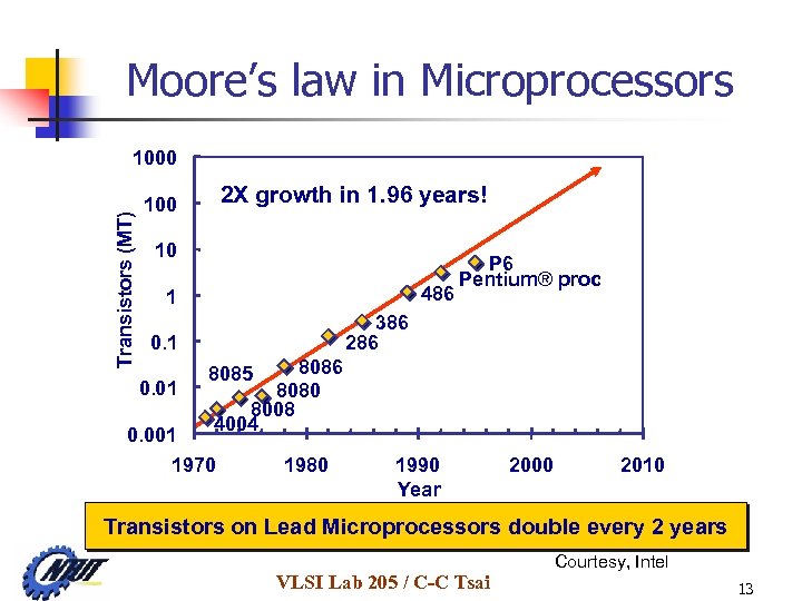 Moore’s law in Microprocessors Transistors (MT) 1000 2 X growth in 1. 96 years! 100 10 486 1 386 286 0. 1 0. 01 P 6 Pentium® proc 8086 8080 8008 4004 8085 0. 001 1970 1980 1990 Year 2000 2010 Transistors on Lead Microprocessors double every 2 years VLSI Lab 205 / C-C Tsai Courtesy, Intel 13
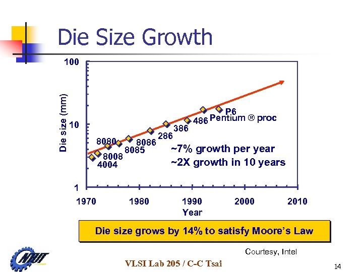 Die Size Growth Die size (mm) 100 10 8080 8008 4004 1 1970 8086 8085 1980 286 386 P 6 Pentium ® proc 486 ~7% growth per year ~2 X growth in 10 years 1990 Year 2000 2010 Die size grows by 14% to satisfy Moore’s Law Courtesy, Intel VLSI Lab 205 / C-C Tsai 14
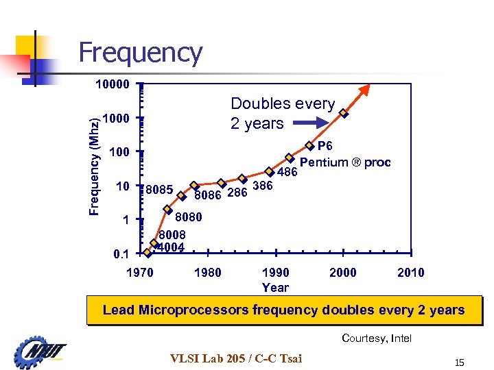 Frequency (Mhz) 10000 Doubles every 2 years 1000 10 8085 1 0. 1 1970 8086 286 386 486 P 6 Pentium ® proc 8080 8008 4004 1980 1990 Year 2000 2010 Lead Microprocessors frequency doubles every 2 years Courtesy, Intel VLSI Lab 205 / C-C Tsai 15
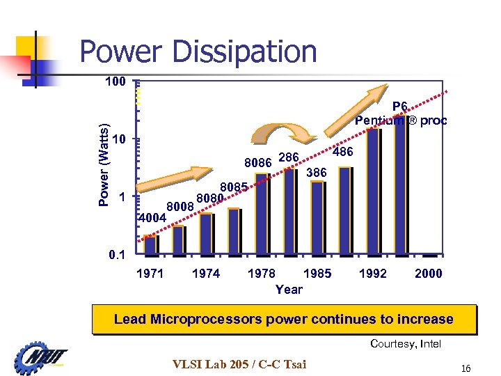 Power Dissipation Power (Watts) 100 P 6 Pentium ® proc 10 8086 286 1 8008 4004 486 386 8085 8080 0. 1 1974 1978 1985 1992 2000 Year Lead Microprocessors power continues to increase Courtesy, Intel VLSI Lab 205 / C-C Tsai 16
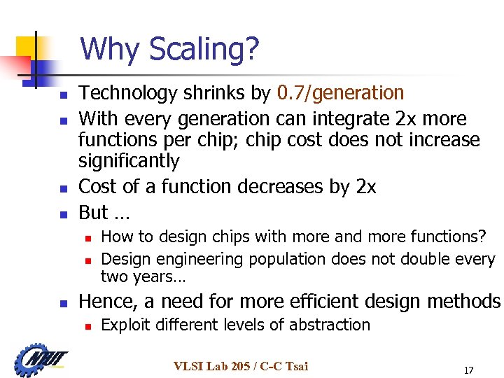 Why Scaling? n n Technology shrinks by 0. 7/generation With every generation can integrate 2 x more functions per chip; chip cost does not increase significantly Cost of a function decreases by 2 x But … n n n How to design chips with more and more functions? Design engineering population does not double every two years… Hence, a need for more efficient design methods n Exploit different levels of abstraction VLSI Lab 205 / C-C Tsai 17
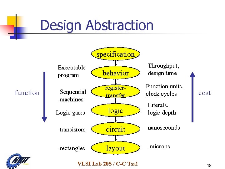 Design Abstraction specification Executable program function Sequential machines Logic gates behavior Throughput, design time registertransfer Function units, clock cycles logic transistors circuit rectangles layout VLSI Lab 205 / C-C Tsai cost Literals, logic depth nanoseconds microns 18
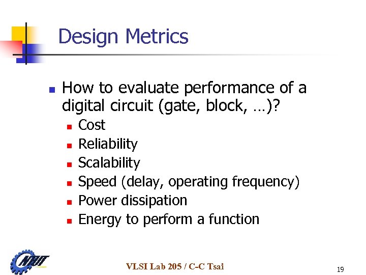 Design Metrics n How to evaluate performance of a digital circuit (gate, block, …)? n n n Cost Reliability Scalability Speed (delay, operating frequency) Power dissipation Energy to perform a function VLSI Lab 205 / C-C Tsai 19
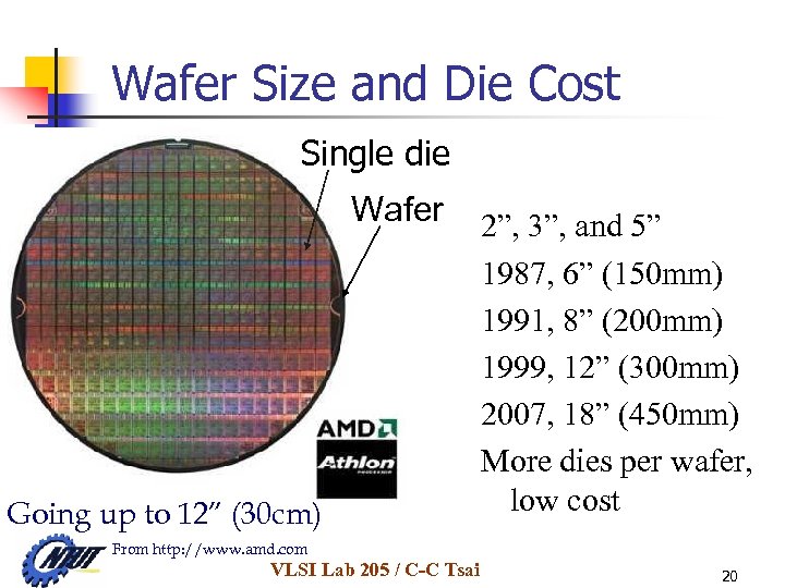 Wafer Size and Die Cost Single die Wafer Going up to 12” (30 cm) 2”, 3”, and 5” 1987, 6” (150 mm) 1991, 8” (200 mm) 1999, 12” (300 mm) 2007, 18” (450 mm) More dies per wafer, low cost From http: //www. amd. com VLSI Lab 205 / C-C Tsai 20
 VLSI View from Research Circular Study n Got ideas for research n Proposal -> grant n Meeting <-> presentation/ brainstorming n Papers: Prepare->submit->revise n Enjoy Research = Enjoy Life !!! VLSI Lab 205 / C-C Tsai 21
 Getting in Research Think to do Re-search for interested topics n Talk with your advisors n n Create new field for research VLSI Lab 205 / C-C Tsai 22
 What Topics for Research n n n n NSC research classifications Call for paper or advanced program Join on workshops, symposiums, and conferences Study papers from journals, letters, magazines, Technique reports, and conferences (Note that future works) MS and Ph. D dissertations Interaction with industries First read recent papers and then go back VLSI Lab 205 / C-C Tsai 23
 Proposal n Grant funding: NSC research project n Co-operational project n NSC case-study student project n MOE VLSI educational project n VLSI Lab 205 / C-C Tsai 24
 Research Resources n n Manpower: graduate and case-study students PCs, workstations, and peripheral devices Professional equipments for testing, observation, and manufacturing Professional tools for simulation, evaluation, graphics, and programming VLSI Lab 205 / C-C Tsai 25
 Materials for Research Journals: IEEE, ACM, IEE, IEICE, . . . n Conferences: IEEE, ACM, VLSI/CAD, ISCAS, CICC, ICCD, ICCAD, DATE, … n Internet: n VLSI Lab 205 / C-C Tsai 26
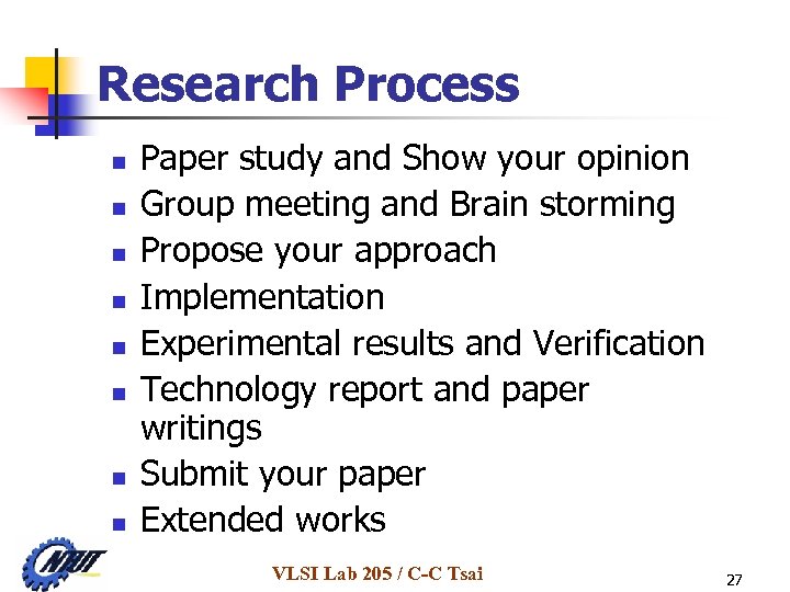 Research Process n n n n Paper study and Show your opinion Group meeting and Brain storming Propose your approach Implementation Experimental results and Verification Technology report and paper writings Submit your paper Extended works VLSI Lab 205 / C-C Tsai 27
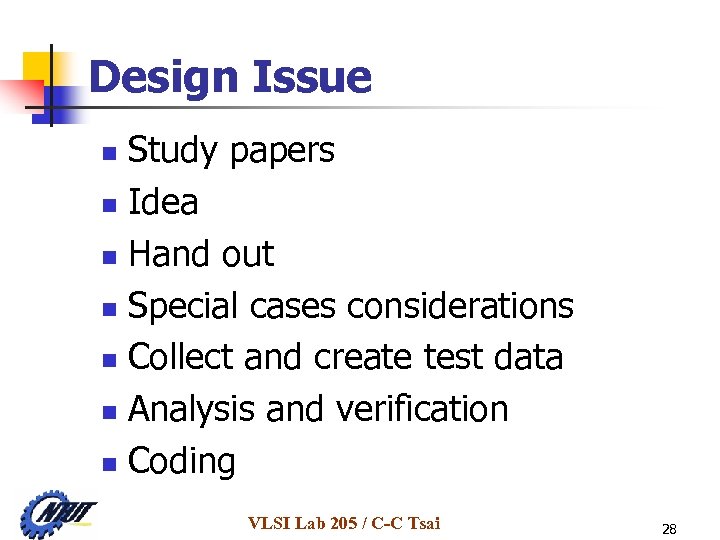 Design Issue Study papers n Idea n Hand out n Special cases considerations n Collect and create test data n Analysis and verification n Coding n VLSI Lab 205 / C-C Tsai 28
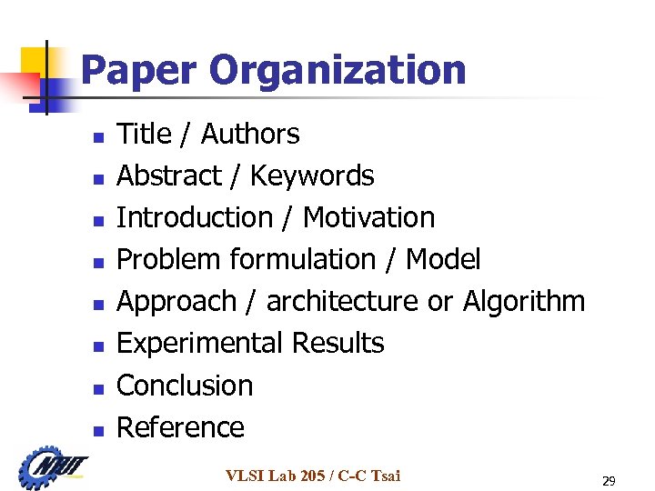 Paper Organization n n n n Title / Authors Abstract / Keywords Introduction / Motivation Problem formulation / Model Approach / architecture or Algorithm Experimental Results Conclusion Reference VLSI Lab 205 / C-C Tsai 29
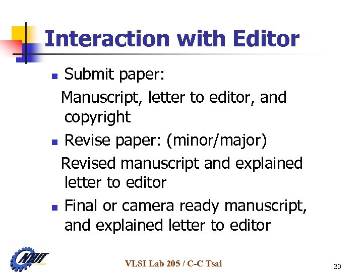 Interaction with Editor Submit paper: Manuscript, letter to editor, and copyright n Revise paper: (minor/major) Revised manuscript and explained letter to editor n Final or camera ready manuscript, and explained letter to editor n VLSI Lab 205 / C-C Tsai 30
 Examples of VLSI Research n n VLSI Design Chip Implementation VLSI CAD EDA-Electronic Design Automation VLSI Lab 205 / C-C Tsai 31
 VLSI Design: Chip Implementation A 10 -bit Switched-Current D/A Converter VLSI Lab 205 / C-C Tsai 32
![Conventional DACs n n Passive-component way a. Resistor strings DAC [Marcel ‘ 90] b. Conventional DACs n n Passive-component way a. Resistor strings DAC [Marcel ‘ 90] b.](https://present5.com/presentation/bb1996b9c0f5534636fdc327ff8f068b/image-33.jpg) Conventional DACs n n Passive-component way a. Resistor strings DAC [Marcel ‘ 90] b. Switched-capacitor DAC [Lin ‘ 96] Active-Component way c. Weighted-current source DAC [Chin ‘ 94] d. Current cell matrix DAC [Yasuyuki ‘ 91] e. Switched-current DAC [Wang ‘ 99] VLSI Lab 205 / C-C Tsai 33
Conventional DACs n n Passive-component way a. Resistor strings DAC [Marcel ‘ 90] b. Switched-capacitor DAC [Lin ‘ 96] Active-Component way c. Weighted-current source DAC [Chin ‘ 94] d. Current cell matrix DAC [Yasuyuki ‘ 91] e. Switched-current DAC [Wang ‘ 99] VLSI Lab 205 / C-C Tsai 33
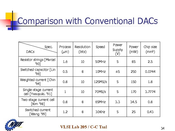 Comparison with Conventional DACs Power Supply (V) Power (m. W) Chip size (mm 2) 50 MHz 5 85 2. 5 8 10 MHz ± 5 250 0. 0744 0. 8 10 125 MS/s 5 150 1. 8 Single-stage current cell [Yasuyuki. ’ 91] 1 10 70 MS/s 5 170 3. 7774 Two-stage current cell [Kim ’ 98] 0. 8 8 65 MHz 3. 3 34. 5 0. 8 Switched-current [Wang ’ 99] 1. 2 8 30 KHz 5 25 0. 43 Process ( m) Resolution (bits) Speed Resistor strings [Marcel ’ 90] 1. 6 10 Switched-capacitor [Lin ’ 96] 0. 5 Weighted-current [Chin ’ 94] Spec. DACs VLSI Lab 205 / C-C Tsai 34
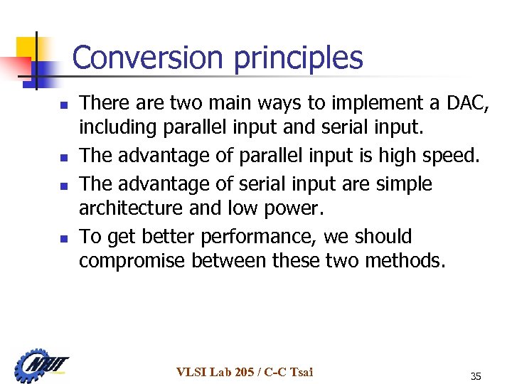 Conversion principles n n There are two main ways to implement a DAC, including parallel input and serial input. The advantage of parallel input is high speed. The advantage of serial input are simple architecture and low power. To get better performance, we should compromise between these two methods. VLSI Lab 205 / C-C Tsai 35
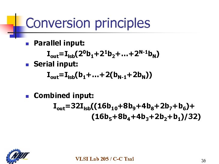 Conversion principles n n n Parallel input: Iout=Ilsb(20 b 1+21 b 2+…+2 N-1 b. N) Serial input: Iout=Ilsb(b 1+…+2(b. N-1+2 b. N)) Combined input: Iout=32 Ilsb((16 b 10+8 b 9+4 b 8+2 b 7+b 6)+ (16 b 5+8 b 4+4 b 3+2 b 2+b 1)/32) VLSI Lab 205 / C-C Tsai 36
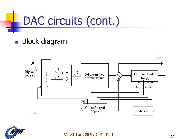 DAC circuits (cont. ) n Block diagram VLSI Lab 205 / C-C Tsai 37
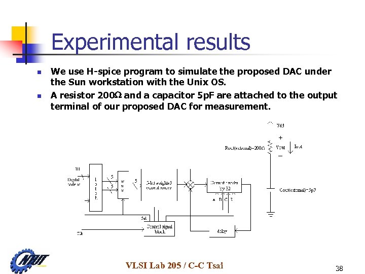 Experimental results n n We use H-spice program to simulate the proposed DAC under the Sun workstation with the Unix OS. A resistor 200 and a capacitor 5 p. F are attached to the output terminal of our proposed DAC for measurement. VLSI Lab 205 / C-C Tsai 38
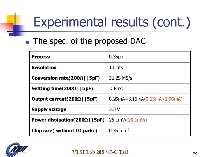 Experimental results (cont. ) n The spec. of the proposed DAC Process 0. 35μm Resolution 10 bits Conversion rate(200 ||5 p. F) 31. 25 MS/s Settling time(200 ||5 p. F) < 8 ns Output current(200 ||5 p. F) 0. 26 m. A~3. 16 m. A(0. 23 m. A~2. 96 m. A) Supply voltage 3. 3 V Power dissipation(200 ||5 p. F) 25. 1 m. W(26. 1 m. W) Chip size( without IO pads ) 0. 35 mm 2 VLSI Lab 205 / C-C Tsai 39
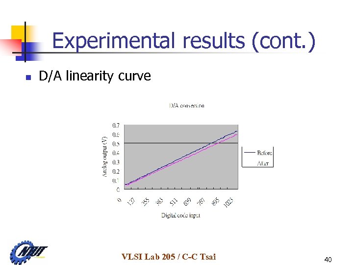 Experimental results (cont. ) n D/A linearity curve VLSI Lab 205 / C-C Tsai 40
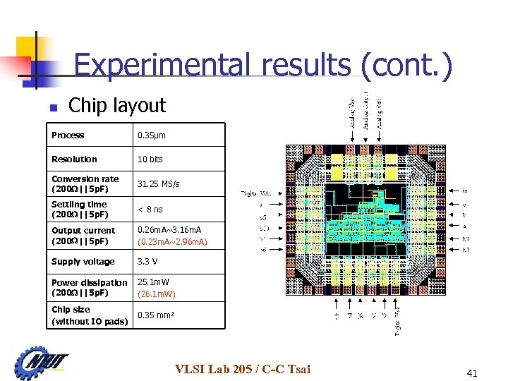 Experimental results (cont. ) n Chip layout Process 0. 35μm Resolution 10 bits Conversion rate (200 ||5 p. F) 31. 25 MS/s Settling time (200 ||5 p. F) < 8 ns Output current (200 ||5 p. F) 0. 26 m. A~3. 16 m. A (0. 23 m. A~2. 96 m. A) Supply voltage 3. 3 V Power dissipation (200 ||5 p. F) 25. 1 m. W (26. 1 m. W) Chip size (without IO pads) 0. 35 mm 2 VLSI Lab 205 / C-C Tsai 41
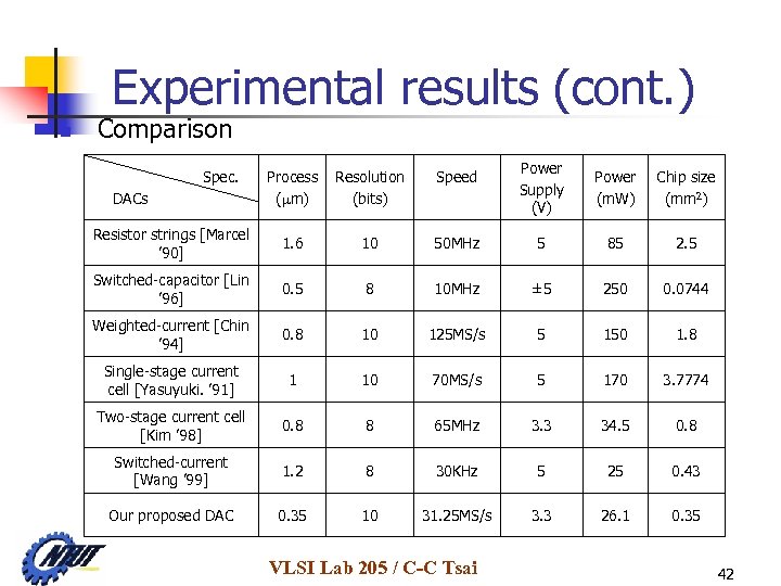 Experimental results (cont. ) n Comparison Power Supply (V) Power (m. W) Chip size (mm 2) 50 MHz 5 85 2. 5 8 10 MHz ± 5 250 0. 0744 0. 8 10 125 MS/s 5 150 1. 8 Single-stage current cell [Yasuyuki. ’ 91] 1 10 70 MS/s 5 170 3. 7774 Two-stage current cell [Kim ’ 98] 0. 8 8 65 MHz 3. 3 34. 5 0. 8 Switched-current [Wang ’ 99] 1. 2 8 30 KHz 5 25 0. 43 Our proposed DAC 0. 35 10 31. 25 MS/s 3. 3 26. 1 0. 35 Process ( m) Resolution (bits) Speed Resistor strings [Marcel ’ 90] 1. 6 10 Switched-capacitor [Lin ’ 96] 0. 5 Weighted-current [Chin ’ 94] Spec. DACs VLSI Lab 205 / C-C Tsai 42
 Future Works n n n Our proposed DAC could expand to 5 N input bits for high resolution requirement in future. It can reach higher speed and lower power dissipation compared with other kinds of switched-current D/A converters. It is applicable to many applications, such as digital TV and computer systems, etc. VLSI Lab 205 / C-C Tsai 43
 VLSI CAD: Electronic Design Automation Clock Routing Methodology Based on Grey Relation Clustering VLSI Lab 205 / C-C Tsai 44
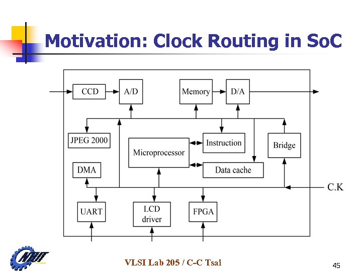 Motivation: Clock Routing in So. C VLSI Lab 205 / C-C Tsai 45
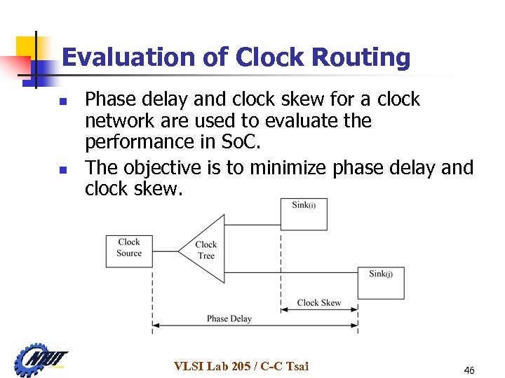 Evaluation of Clock Routing n n Phase delay and clock skew for a clock network are used to evaluate the performance in So. C. The objective is to minimize phase delay and clock skew. VLSI Lab 205 / C-C Tsai 46
 Problem Definition Four clock routing problems defined as below: n Problem 1: Clock global routing n A set of clock terminals distributed on a plane, the objective is to construct a clock tree with minimum clock delay and clock skew in global routing. VLSI Lab 205 / C-C Tsai 47
 Problem Definition (Cont’d) n Problem 2: Clock detailed routing n n n A module consists of a set of blocks distributed within the module plane and has a clock source located on any boundary of the module. The objective is to construct a clock tree and to connect the clock source and sinks with minimum clock delay and clock skew in detailed routing. Problem 3: Clock detailed routing with buffers insertion. n Like the statement of Problem 2, the objective is to construct a clock tree and to connect the clock source and clock sinks in the limitation of the clock skew ratio under 5% with minimum clock delay by inserting buffers in detailed routing. VLSI Lab 205 / C-C Tsai 48
 Problem Definition (Cont’d) n Problem 4: Clock detailed routing in So. C level. n n A So. C consists of a set of IPs including modules distributed within the So. C plane and has a system clock source located on the So. C any boundary. The objective is to construct a system clock tree and to connect the system clock source and all the clock sinks in the limitation of the clock skew ratio under 5% with minimum system clock delay by inserting buffers in detailed routing. VLSI Lab 205 / C-C Tsai 49
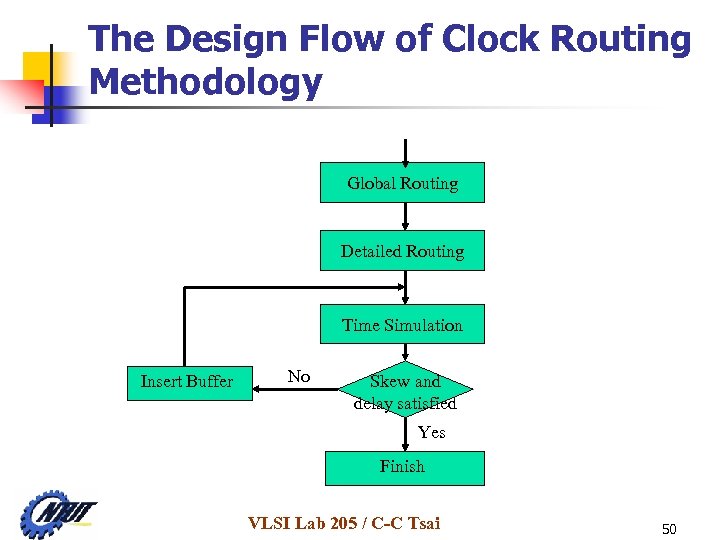 The Design Flow of Clock Routing Methodology Global Routing Detailed Routing Time Simulation Insert Buffer No Skew and delay satisfied Yes Finish VLSI Lab 205 / C-C Tsai 50
 Clock Global Routing for Problem 1 n n Grey theory is first investigated. [Teng, ’ 96] We employ the grey relational analysis method to help us to determine each pair of clustering sinks and to construct a clock tree with the minimizations of clock delay and skew. VLSI Lab 205 / C-C Tsai 51
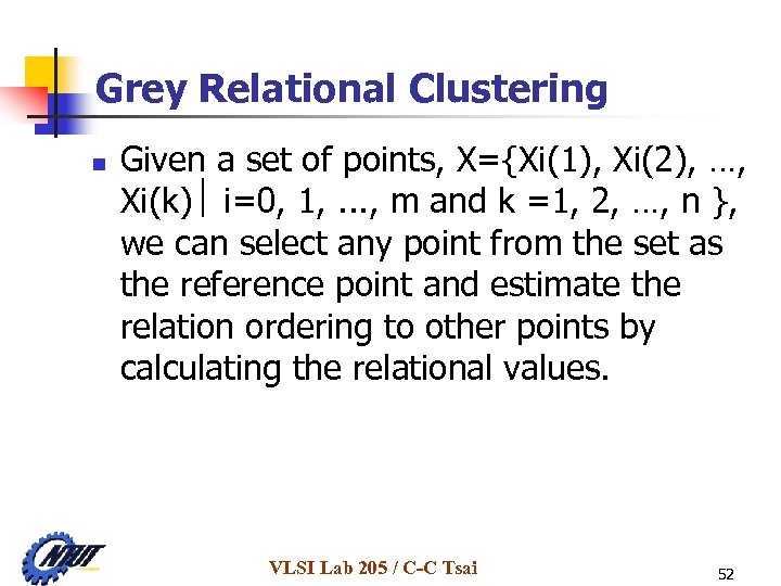 Grey Relational Clustering n Given a set of points, X={Xi(1), Xi(2), …, Xi(k) i=0, 1, . . . , m and k =1, 2, …, n }, we can select any point from the set as the reference point and estimate the relation ordering to other points by calculating the relational values. VLSI Lab 205 / C-C Tsai 52
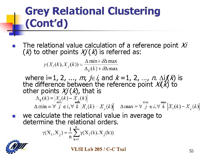 Grey Relational Clustering (Cont’d) n The relational value calculation of a reference point Xi (k) to other points Xj (k) is referred as: where i=1, 2, . . . , m, j i, and k =1, 2, …, n. ij(k) is the difference between the reference point Xi(k) to other points Xj (k), that is n we calculate the relational value in average to determine the relational orders. VLSI Lab 205 / C-C Tsai 53
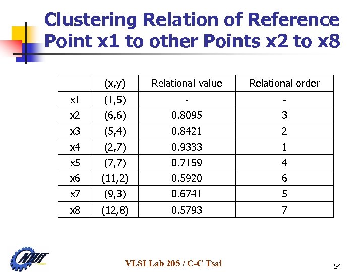 Clustering Relation of Reference Point x 1 to other Points x 2 to x 8 (x, y) Relational value Relational order x 1 (1, 5) - - x 2 (6, 6) 0. 8095 3 x 3 (5, 4) 0. 8421 2 x 4 (2, 7) 0. 9333 1 x 5 (7, 7) 0. 7159 4 x 6 (11, 2) 0. 5920 6 x 7 (9, 3) 0. 6741 5 x 8 (12, 8) 0. 5793 7 VLSI Lab 205 / C-C Tsai 54
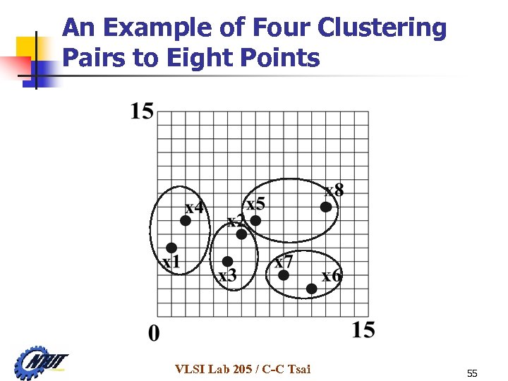 An Example of Four Clustering Pairs to Eight Points VLSI Lab 205 / C-C Tsai 55
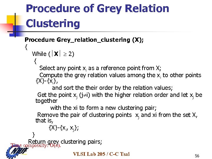 Procedure of Grey Relation Clustering Procedure Grey_relation_clustering (X); { While ( X 2) { Select any point xi as a reference point from X; Compute the grey relation values among the xi to other points {X}-{xi}, and sort their order by the relation values; Get the point xj (j i) with the higher relation order and let xj be together with the xi to form a new clustering pair; Remove the pair of clustering points xj and xi from the set X, that is, {X}-{xi, xj}; } Return grey clustering pairs; Time complexity: O(n). } VLSI Lab 205 / C-C Tsai 56
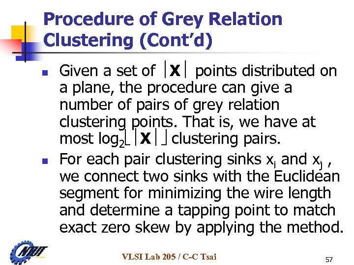 Procedure of Grey Relation Clustering (Cont’d) n n Given a set of X points distributed on a plane, the procedure can give a number of pairs of grey relation clustering points. That is, we have at most log 2 X clustering pairs. For each pair clustering sinks xi and xj , we connect two sinks with the Euclidean segment for minimizing the wire length and determine a tapping point to match exact zero skew by applying the method. VLSI Lab 205 / C-C Tsai 57
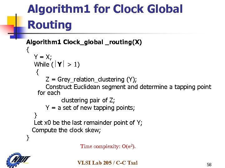 Algorithm 1 for Clock Global Routing Algorithm 1 Clock_global _routing(X) { Y = X; While ( Y > 1) { Z = Grey_relation_clustering (Y); Construct Euclidean segment and determine a tapping point for each clustering pair of Z; Y = a set of new tapping points; } Let x 0 be the last remainder point of Y; Compute the clock skew; } Time complexity: O(n 2). VLSI Lab 205 / C-C Tsai 58
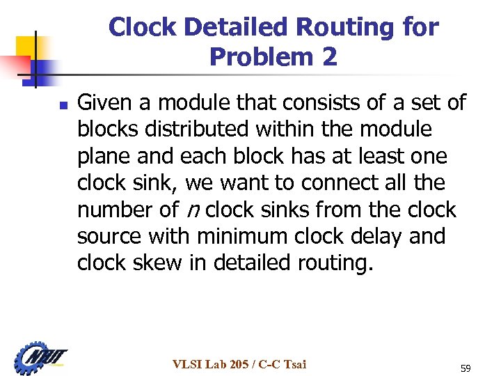 Clock Detailed Routing for Problem 2 n Given a module that consists of a set of blocks distributed within the module plane and each block has at least one clock sink, we want to connect all the number of n clock sinks from the clock source with minimum clock delay and clock skew in detailed routing. VLSI Lab 205 / C-C Tsai 59
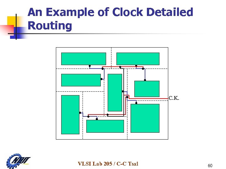 An Example of Clock Detailed Routing C. K. VLSI Lab 205 / C-C Tsai 60
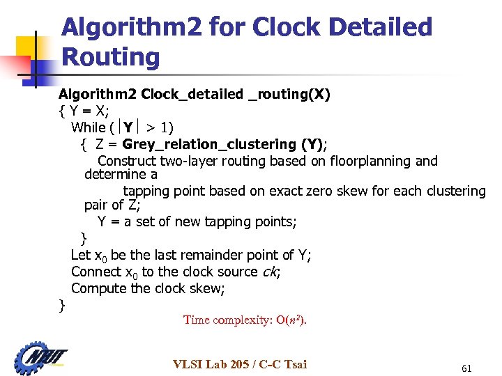 Algorithm 2 for Clock Detailed Routing Algorithm 2 Clock_detailed _routing(X) { Y = X; While ( Y > 1) { Z = Grey_relation_clustering (Y); Construct two-layer routing based on floorplanning and determine a tapping point based on exact zero skew for each clustering pair of Z; Y = a set of new tapping points; } Let x 0 be the last remainder point of Y; Connect x 0 to the clock source ck; Compute the clock skew; } Time complexity: O(n 2). VLSI Lab 205 / C-C Tsai 61
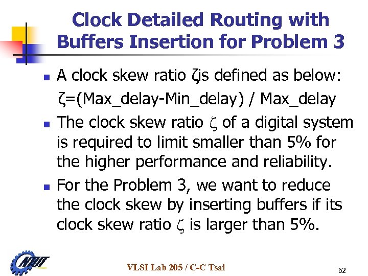 Clock Detailed Routing with Buffers Insertion for Problem 3 n n n A clock skew ratio ζis defined as below: ζ=(Max_delay-Min_delay) / Max_delay The clock skew ratio of a digital system is required to limit smaller than 5% for the higher performance and reliability. For the Problem 3, we want to reduce the clock skew by inserting buffers if its clock skew ratio is larger than 5%. VLSI Lab 205 / C-C Tsai 62
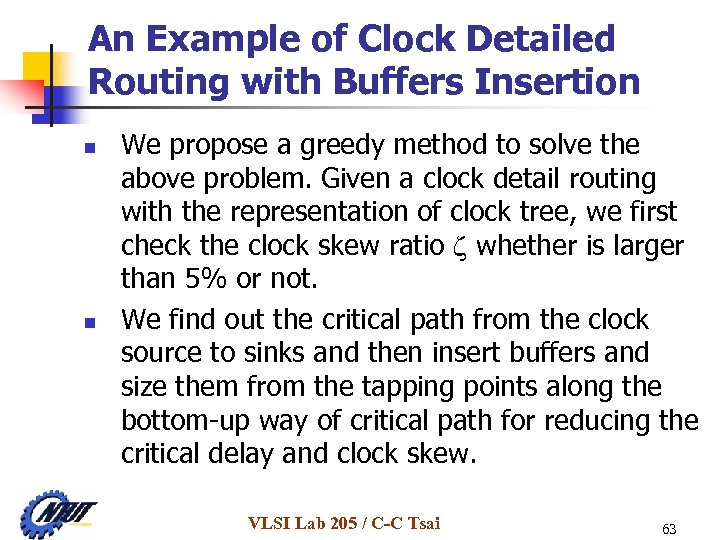 An Example of Clock Detailed Routing with Buffers Insertion n n We propose a greedy method to solve the above problem. Given a clock detail routing with the representation of clock tree, we first check the clock skew ratio whether is larger than 5% or not. We find out the critical path from the clock source to sinks and then insert buffers and size them from the tapping points along the bottom-up way of critical path for reducing the critical delay and clock skew. VLSI Lab 205 / C-C Tsai 63
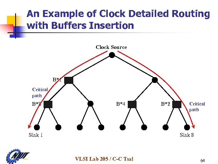 An Example of Clock Detailed Routing with Buffers Insertion Clock Source B*1 Critical path B*8 B*4 Sink 1 B*2 B*1 Critical path Sink 8 VLSI Lab 205 / C-C Tsai 64
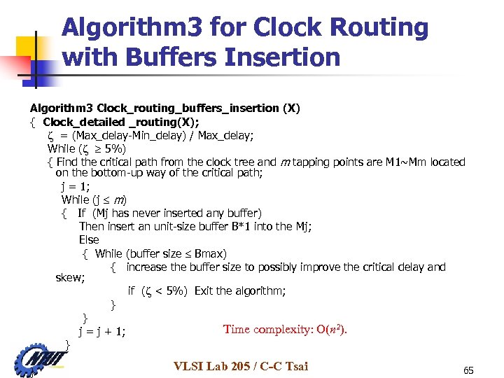 Algorithm 3 for Clock Routing with Buffers Insertion Algorithm 3 Clock_routing_buffers_insertion (X) { Clock_detailed _routing(X); = (Max_delay-Min_delay) / Max_delay; While ( 5%) { Find the critical path from the clock tree and m tapping points are M 1~Mm located on the bottom-up way of the critical path; j = 1; While (j m) { If (Mj has never inserted any buffer) Then insert an unit-size buffer B*1 into the Mj; Else { While (buffer size Bmax) { increase the buffer size to possibly improve the critical delay and skew; if ( < 5%) Exit the algorithm; } } Time complexity: O(n 2). j = j + 1; } } VLSI Lab 205 / C-C Tsai 65 }
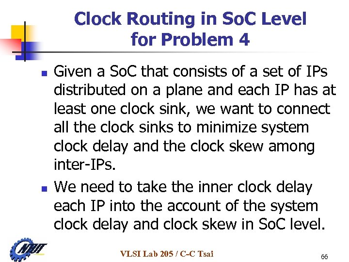 Clock Routing in So. C Level for Problem 4 n n Given a So. C that consists of a set of IPs distributed on a plane and each IP has at least one clock sink, we want to connect all the clock sinks to minimize system clock delay and the clock skew among inter-IPs. We need to take the inner clock delay each IP into the account of the system clock delay and clock skew in So. C level. VLSI Lab 205 / C-C Tsai 66
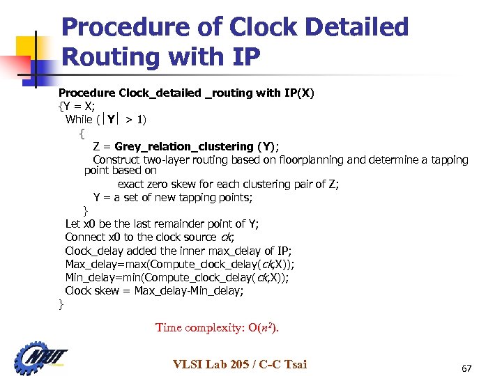 Procedure of Clock Detailed Routing with IP Procedure Clock_detailed _routing with IP(X) {Y = X; While ( Y > 1) { Z = Grey_relation_clustering (Y); Construct two-layer routing based on floorplanning and determine a tapping point based on exact zero skew for each clustering pair of Z; Y = a set of new tapping points; } Let x 0 be the last remainder point of Y; Connect x 0 to the clock source ck; Clock_delay added the inner max_delay of IP; Max_delay=max(Compute_clock_delay(ck, X)); Min_delay=min(Compute_clock_delay(ck, X)); Clock skew = Max_delay-Min_delay; } Time complexity: O(n 2). VLSI Lab 205 / C-C Tsai 67
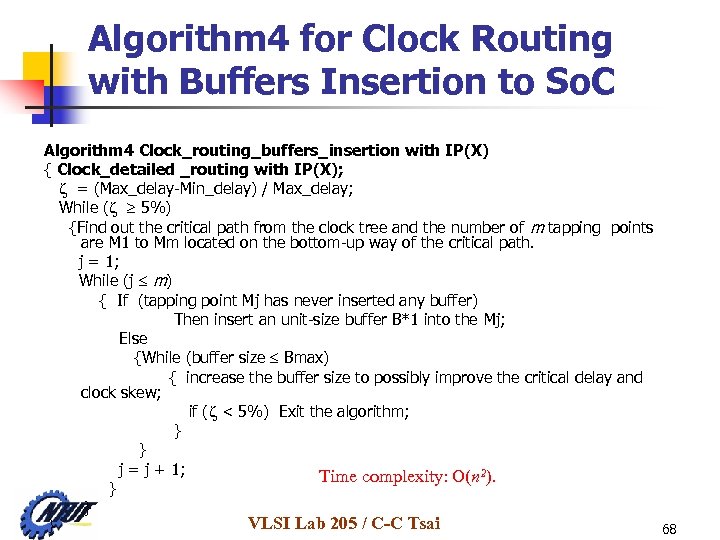 Algorithm 4 for Clock Routing with Buffers Insertion to So. C Algorithm 4 Clock_routing_buffers_insertion with IP(X) { Clock_detailed _routing with IP(X); = (Max_delay-Min_delay) / Max_delay; While ( 5%) {Find out the critical path from the clock tree and the number of m tapping points are M 1 to Mm located on the bottom-up way of the critical path. j = 1; While (j m) { If (tapping point Mj has never inserted any buffer) Then insert an unit-size buffer B*1 into the Mj; Else {While (buffer size Bmax) { increase the buffer size to possibly improve the critical delay and clock skew; if ( < 5%) Exit the algorithm; } } j = j + 1; Time complexity: O(n 2). } } } VLSI Lab 205 / C-C Tsai 68
 The Parameters of 0. 18μm Technology r unit resistance of a wire 0. 075Ω/ m c t. B unit capacitance of a wire 0. 118 f. F/ m intrinsic delay for a unit buffer 36. 4 ps c. B input capacitance of a unit buffer 23. 4 f. F r. B output resistance of a unit buffer 180Ω VLSI Lab 205 / C-C Tsai 69
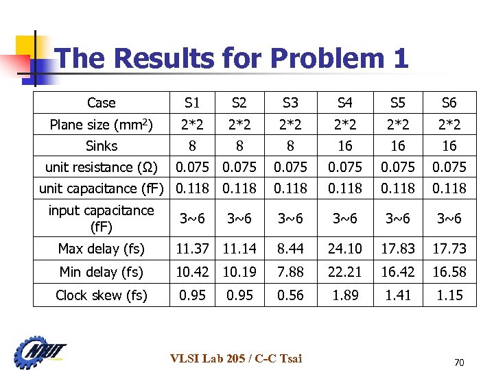 The Results for Problem 1 Case S 1 S 2 S 3 S 4 S 5 S 6 Plane size (mm 2) 2*2 2*2 2*2 Sinks 8 8 8 16 16 16 0. 075 unit capacitance (f. F) 0. 118 3~6 3~6 unit resistance (Ω) input capacitance (f. F) 3~6 Max delay (fs) 11. 37 11. 14 8. 44 24. 10 17. 83 17. 73 Min delay (fs) 10. 42 10. 19 7. 88 22. 21 16. 42 16. 58 0. 95 0. 56 1. 89 1. 41 1. 15 Clock skew (fs) 0. 95 VLSI Lab 205 / C-C Tsai 70
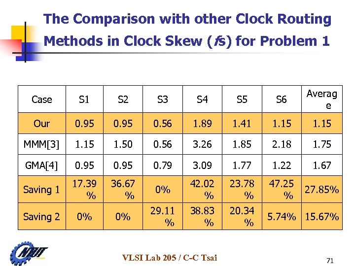 The Comparison with other Clock Routing Methods in Clock Skew (fs) for Problem 1 Case S 1 S 2 S 3 S 4 S 5 S 6 Averag e Our 0. 95 0. 56 1. 89 1. 41 1. 15 MMM[3] 1. 15 1. 50 0. 56 3. 26 1. 85 2. 18 1. 75 GMA[4] 0. 95 0. 79 3. 09 1. 77 1. 22 1. 67 Saving 1 17. 39 % 36. 67 % 0% 42. 02 % 23. 78 % 47. 25 % 27. 85% Saving 2 0% 0% 29. 11 % 38. 83 % 20. 34 % 5. 74% 15. 67% VLSI Lab 205 / C-C Tsai 71
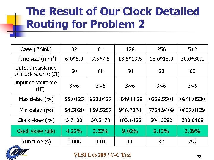 The Result of Our Clock Detailed Routing for Problem 2 Case (#Sink) 32 64 128 256 512 Plane size (mm 2) 6. 0*6. 0 7. 5*7. 5 13. 5*13. 5 15. 0*15. 0 30. 0*30. 0 output resistance of clock source (Ω) 60 60 60 input capacitance (f. F) 3~6 3~6 3~6 Max delay (ps) 88. 0123 920. 0427 1049. 8829 8229. 5501 8940. 8538 Min delay (ps) 84. 3020 889. 5257 946. 7374 7724. 9409 8637. 8129 Clock skew (ps) 3. 7103 30. 5170 103. 1455 504. 6092 303. 0409 Clock skew ratio 4. 22% 3. 32% 9. 82% 6. 13% 3. 39% Run time (s) 0. 006 0. 01 11 87 757 VLSI Lab 205 / C-C Tsai 72
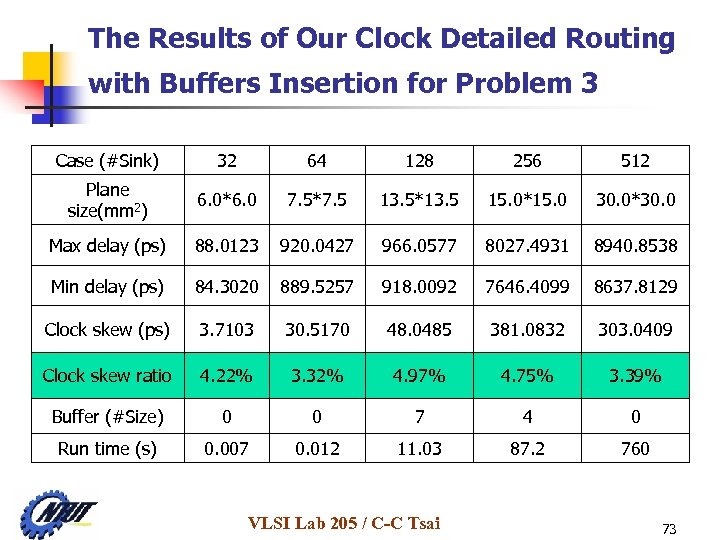 The Results of Our Clock Detailed Routing with Buffers Insertion for Problem 3 Case (#Sink) 32 64 128 256 512 Plane size(mm 2) 6. 0*6. 0 7. 5*7. 5 13. 5*13. 5 15. 0*15. 0 30. 0*30. 0 Max delay (ps) 88. 0123 920. 0427 966. 0577 8027. 4931 8940. 8538 Min delay (ps) 84. 3020 889. 5257 918. 0092 7646. 4099 8637. 8129 Clock skew (ps) 3. 7103 30. 5170 48. 0485 381. 0832 303. 0409 Clock skew ratio 4. 22% 3. 32% 4. 97% 4. 75% 3. 39% Buffer (#Size) 0 0 7 4 0 Run time (s) 0. 007 0. 012 11. 03 87. 2 760 VLSI Lab 205 / C-C Tsai 73
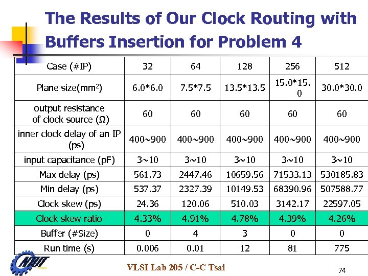 The Results of Our Clock Routing with Buffers Insertion for Problem 4 Case (#IP) 32 64 128 256 512 Plane size(mm 2) 6. 0*6. 0 7. 5*7. 5 13. 5*13. 5 15. 0*15. 0 30. 0*30. 0 output resistance of clock source (Ω) 60 60 60 400~900 3~10 inner clock delay of an IP 400~900 (ps) input capacitance (p. F) 3~10 Max delay (ps) 561. 73 2447. 46 10659. 56 71533. 13 530185. 83 Min delay (ps) 537. 37 2327. 39 10149. 53 68390. 96 507588. 77 Clock skew (ps) 24. 36 120. 06 510. 03 3142. 17 22597. 05 Clock skew ratio 4. 33% 4. 91% 4. 78% 4. 39% 4. 26% Buffer (#Size) 0 4 3 0 0 Run time (s) 0. 006 0. 01 12 81 775 VLSI Lab 205 / C-C Tsai 74
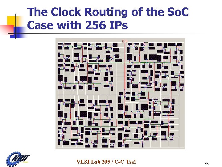 The Clock Routing of the So. C Case with 256 IPs VLSI Lab 205 / C-C Tsai 75
 Future Works n More extended works will be considered in advance, such as the RLC mode for a wire, multi-clock tree routing, and crosstalk reduction for multi-clock routing in So. C. VLSI Lab 205 / C-C Tsai 76
 VLSI View from Chip Design U 05 -87 D梯 次 (教 育 性 晶 片 經 由 Tanner Tool之 S-Edit, T -Spice與 L-Edit, 再由 Dracula進行驗證 作 ) • 實務專題 (李文達副教授 ) 01 E---四位元全加法器 /張維修 02 E---標準元件閘設計 /林志修 • 實務專題 (蔡加春教授 ) 03 E---三個匯流排重複器 (5 V Size 1)/江雨潔與郭淑 華 • 實務專題 (蔡加春教授 ) 用 FPGA實現數位邏輯分析卡 /史振生 用 FPGA實現超任的遊戲搖桿控制器 /王仁煌 VLSI Lab 205 / C-C Tsai 77
 U 05 -88 B梯次 • 實務專題 (蔡加春教授 /李文達副教授 ) 02 E---特博碼解碼器製作 /林文威 04 E---可調式頻率計數晶片設計 /簡文彬 03 E---低電壓匯流排重複器 /黃本松與紀智倫 • 超大型積体電路導論 (蔡加春教授 ) 14 E---可擴充比較器 /陳朝偉等 4位 15 E---具有重置功能的上下計數器 /郭俊宏等 3位 16 E ---四位元比較器 /陳昭興等 4位 17 E---數位暫存器 /李威德等 4位 18 E---四位元移位暫存器 /謝啟仁等 4位 VLSI Lab 205 / C-C Tsai 78
 U 05 -89 A梯次 • 電腦輔助積體電路設計 (蔡加春教授 ) 03 E---二相步進馬達驅動控制器 /吳占鰲 • 實務專題 (李文達副教授 ) 06 E---四位元低電壓符號選擇式布斯乘法器 /江文 盛 U 05 -89 B梯次 • 實務專題 (蔡加春教授 /李文達副教授 ) 02 E---八位元改良式布斯乘法器 /江文盛 03 E---高速腓特比解碼器晶片製作 /林桂蘭 04 E---高速循環碼編碼器 &解碼器晶片設計與製作 /周 淑嫻 07 E---高增益高頻帶寬度 作於低電壓運算放大器 /林 忠信 08 E---低電壓 D/A Converter 晶片製作 /黃志雄 09 E---低電壓 Op-Amp 之製作 /林文彬 VLSI Lab 205 / C-C Tsai 79
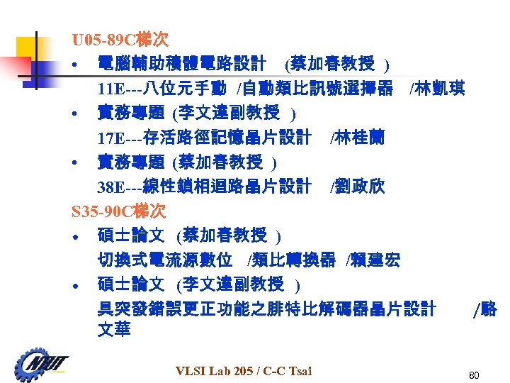 U 05 -89 C梯次 • 電腦輔助積體電路設計 (蔡加春教授 ) 11 E---八位元手動 /自動類比訊號選擇器 /林凱琪 • 實務專題 (李文達副教授 ) 17 E---存活路徑記憶晶片設計 /林桂蘭 • 實務專題 (蔡加春教授 ) 38 E---線性鎖相迴路晶片設計 /劉政欣 S 35 -90 C梯次 • 碩士論文 (蔡加春教授 ) 切換式電流源數位 /類比轉換器 /賴建宏 • 碩士論文 (李文達副教授 ) 具突發錯誤更正功能之腓特比解碼器晶片設計 /駱 文華 VLSI Lab 205 / C-C Tsai 80
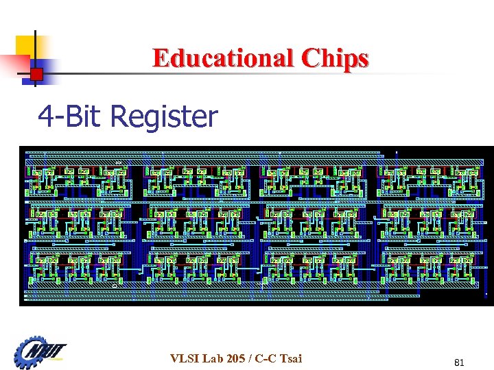 Educational Chips 4 -Bit Register VLSI Lab 205 / C-C Tsai 81
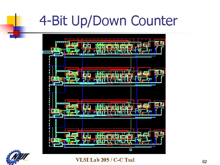 4 -Bit Up/Down Counter VLSI Lab 205 / C-C Tsai 82
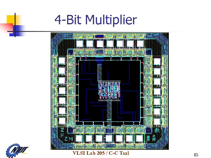 4 -Bit Multiplier VLSI Lab 205 / C-C Tsai 83
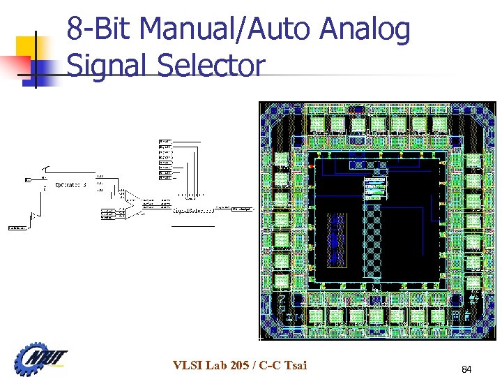 8 -Bit Manual/Auto Analog Signal Selector VLSI Lab 205 / C-C Tsai 84
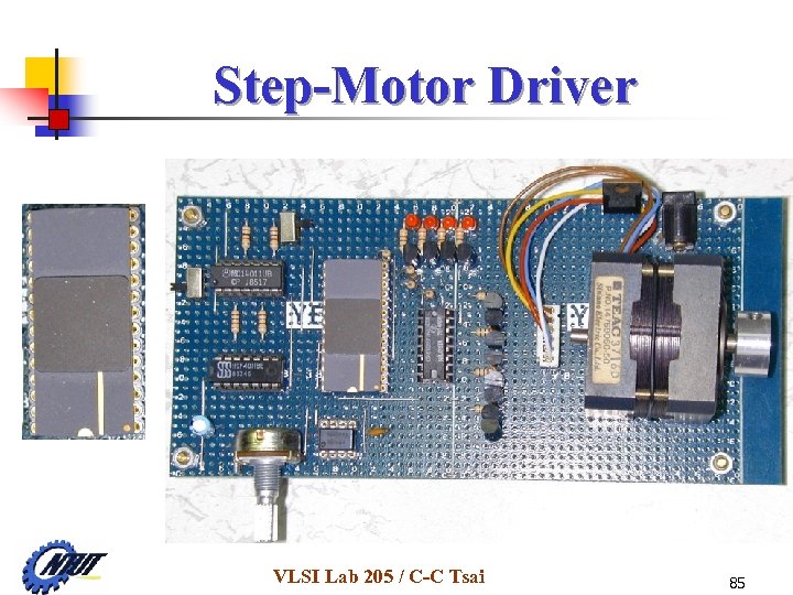 Step-Motor Driver VLSI Lab 205 / C-C Tsai 85
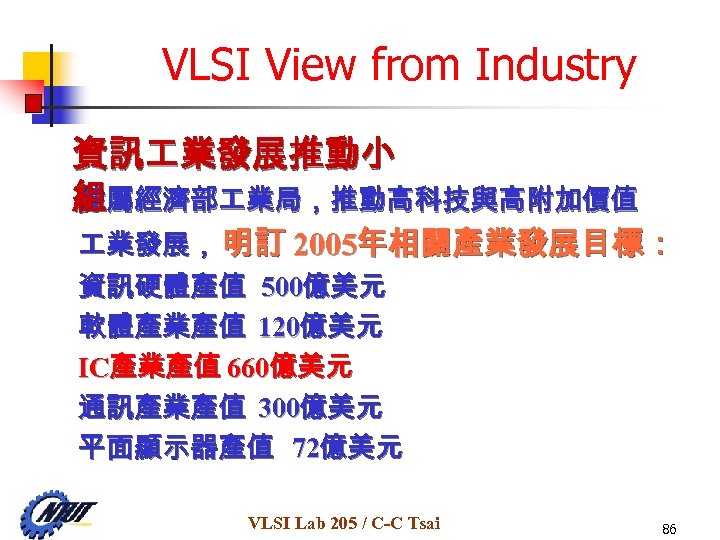 VLSI View from Industry 資訊 業發展推動小 隸屬經濟部 業局,推動高科技與高附加價值 組 業發展, 明訂 2005年相關產業發展目標: 資訊硬體產值 500億美元 軟體產業產值 120億美元 IC產業產值 660億美元 通訊產業產值 300億美元 平面顯示器產值 72億美元 VLSI Lab 205 / C-C Tsai 86
 新興半導體應用產品 除 PC是最主要應用 ,還有很多相關產品 : • DVD相 關 產 品 方 面 : DVD-ROM, DVD Servo/Data processing晶片組。 • 寬 頻 網 路 相 關 產品 方 面 : Cable Modem、 x. DSL Modem、 Automobile Navigation System、 Digital DSC(Digital Still Camera)等產品。 Camcorder、 • 數 位 STB方 面 : 結 合 DVD、Cable Modem 、Game 、 Digital TV等 功 能 , 上 處 理 功 能 越 來 越 強 大 的 MPU(32 bit 加 以上 ), STB將會成為家庭中的 Entertainment PC。 • 大哥大手機方面 : 大哥大手機的晶片組研發。 VLSI Lab 205 / C-C Tsai 87
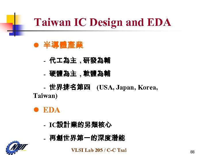 Taiwan IC Design and EDA l 半導體產業 - 代 為主 , 研發為輔 - 硬體為主 , 軟體為輔 - 世界排名第四 (USA, Japan, Korea, Taiwan) l EDA - IC設計業的另類核心 - 再創世界第一的深度潛能 VLSI Lab 205 / C-C Tsai 88
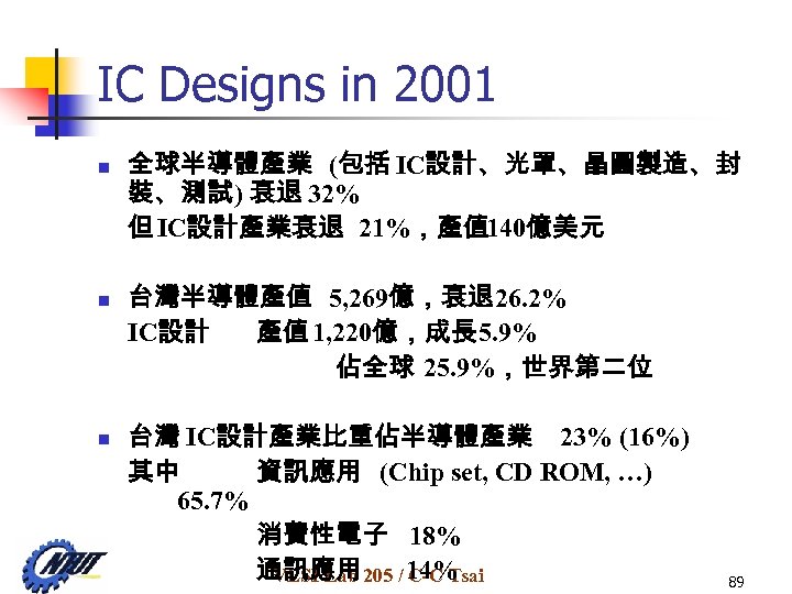 IC Designs in 2001 n n n 全球半導體產業 (包括 IC設計、光罩、晶圓製造、封 裝、測試) 衰退 32% 但 IC設計產業衰退 21%,產值 140億美元 台灣半導體產值 5, 269億,衰退26. 2% IC設計 產值 1, 220億,成長 5. 9% 佔全球 25. 9%,世界第二位 台灣 IC設計產業比重佔半導體產業 23% (16%) 其中 資訊應用 (Chip set, CD ROM, …) 65. 7% 消費性電子 18% 通訊應用 205 / 14% VLSI Lab C-C Tsai 89
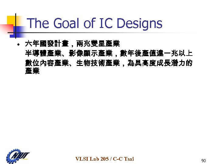 The Goal of IC Designs • 六年國發計畫,兩兆雙星產業 半導體產業、影像顯示產業,數年後產值達一兆以上 數位內容產業、生物技術產業,為具高度成長潛力的 產業 VLSI Lab 205 / C-C Tsai 90
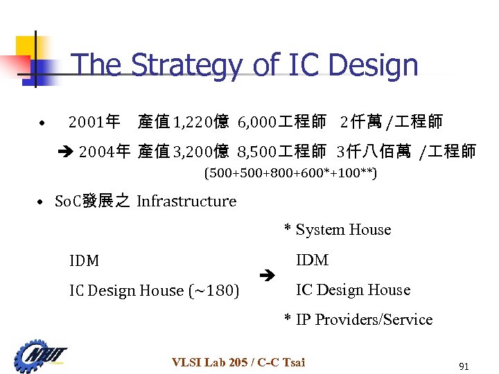 The Strategy of IC Design • 2001年 產值 1, 220億 6, 000 程師 2仟萬 / 程師 2004年 產值 3, 200億 8, 500 程師 3仟八佰萬 / 程師 (500+800+600*+100**) • So. C發展之 Infrastructure * System House IDM IC Design House (~180) IDM IC Design House * IP Providers/Service VLSI Lab 205 / C-C Tsai 91
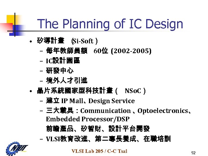 The Planning of IC Design • 矽導計畫 ( Si-Soft) – 每年教師員額 60位 (2002 -2005) – IC設計園區 – 研發中心 – 境外人才引進 • 晶片系統國家型科技計畫( NSo. C) – 建立 IP Mall、 Design Service – 三大載具:Communication 、 Optoelectronics、 Embedded Processor/DSP 前瞻產品、矽智財、設計平台開發 – VLSI教育改進、第二專長養成、在職培訓 VLSI Lab 205 / C-C Tsai 92
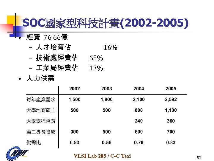 SOC國家型科技計畫(2002 -2005) • 經費 76. 66億 – 人才培育佔 – 技術處經費佔 – 業局經費佔 • 人力供需 16% 65% 13% VLSI Lab 205 / C-C Tsai 93
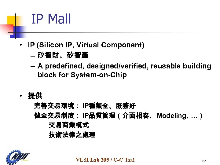 IP Mall • IP (Silicon IP, Virtual Component) – 矽智財、矽智產 – A predefined, designed/verified, reusable building block for System-on-Chip • 提供 完善交易環境: IP種類全、服務好 健全交易制度: IP品質管理(介面相容、 Modeling、 …) 交易商業模式 技術法律之處理 VLSI Lab 205 / C-C Tsai 94
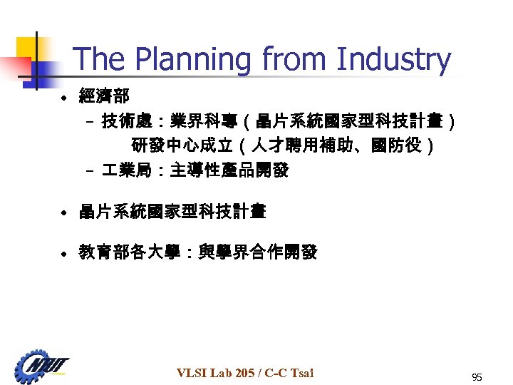 The Planning from Industry • 經濟部 – 技術處:業界科專(晶片系統國家型科技計畫) 研發中心成立(人才聘用補助、國防役) – 業局:主導性產品開發 • 晶片系統國家型科技計畫 • 教育部各大學:與學界合作開發 VLSI Lab 205 / C-C Tsai 95
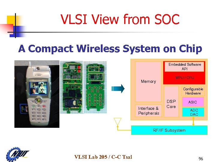 VLSI View from SOC A Compact Wireless System on Chip Embedded Software API Memory MPU / CPU Configurable Hardware Interface & Peripherals DSP Core ASIC ADC DAC RF/IF Subsystem VLSI Lab 205 / C-C Tsai 96
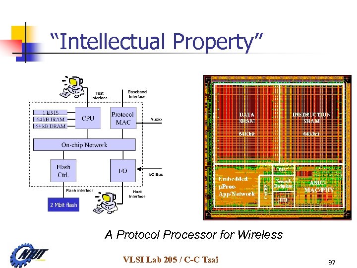 “Intellectual Property” A Protocol Processor for Wireless VLSI Lab 205 / C-C Tsai 97
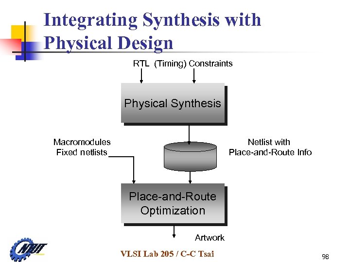 Integrating Synthesis with Physical Design RTL (Timing) Constraints Physical Synthesis Macromodules Fixed netlists Netlist with Place-and-Route Info Place-and-Route Optimization Artwork VLSI Lab 205 / C-C Tsai 98
 So. C: System on Chip n System A collection of all kinds of components and/or subsystems that are appropriately interconnected to perform the specified functions for end users. n A So. C design is a “product creation process” which n n Starts at identifying the end-user needs Ends at delivering a product with enough functional satisfaction to overcome the payment from the end-user VLSI Lab 205 / C-C Tsai 99
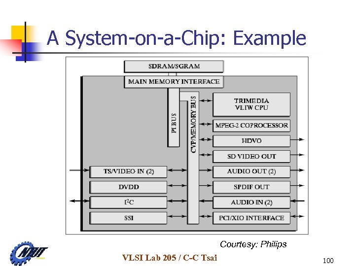 A System-on-a-Chip: Example Courtesy: Philips VLSI Lab 205 / C-C Tsai 100
 Silicon Integration Functional integration - signal processing communication, multimedia standards - human interactions - system resources coordination n IC technology - 0. 18, 0. 13, 0. 10, 0. 08 micron, … - e. g. 0. 18 micron 60 GHz cutoff frequency n VLSI Lab 205 / C-C Tsai 101
 Challenges in So. C Era n Time-to-market n n n Silicon Complexity n n n Heterogeneous processes Billion Txs, Deep submicron effects : crosstalk, wire delays, electromigration, mask costs Design Complexity n n n Process roadmap acceleration Consumerization of electronic devices Cs, DSPs, HW/SW, SW protocol stacks, RTOS’s, digital/analog IPs, On-chips buses System-level architecture Time-in-market n n Performance/Energy/Cost tradeoff Scalable architecture with unified design environment VLSI Lab 205 / C-C Tsai 102
 How to Conquer the Complexity n Use a known real entity n n n Partition n A pre-designed component (IP reuse) A platform (architecture reuse) Based on functionality Hardware and software Modeling n n At different level Consistent and accurate VLSI Lab 205 / C-C Tsai 103
 Platform n n A fully defined bus structure and a collection of IP blocks A design methodology to support the feature of “Plugging and Playing” The definition of a platform is the result of a trade-off process involving reusability (programmability and configurability), cost and performance optimization. Enhance the differentiation VLSI Lab 205 / C-C Tsai 104
 Core Technologies n n n IP Development System Architecture So. C Verification Embedded Software High Speed/Low Power Design VLSI Lab 205 / C-C Tsai 105
 IP n n A predefined, designed/verified, reusable building block for System-on-Chip Software IP, Silicon IP (Soft IP, Hard IP, …) IP types n Foundation IP (cell library, gate array) n Standard IP (MPEG 2/4, JPEG, USB, IEEE 1394, PCI…) n Star IP (ARM, MIPS, Rambus, …) Ancillary characteristics n Deliverable at certain level, software/hardware interfaces n Modeling at different levels n Customizable, Configurable, Parameterizable VLSI Lab 205 / C-C Tsai 106
 System Architecture Design n Specification, Requirement, Functionalities Architecture C-level design, System. C description and simulation Advantage n Broader design space performance, power, cost tradeoff scalability, good for time-in-market n Early verification module well-define, partition, refinement necessary for time-to-market VLSI Lab 205 / C-C Tsai 107
 Architecture Re. Use n n n Silicon System Platform n Flexible architecture for hardware and software n Specific (programmable) components n Network architecture n Software modules n Rules and guidelines for design of HW and SW Has been successful in PC’s n Dominance of a few players who specify and control architecture Application-domain specific (difference in constraints) n Speed (compute power) n Dissipation n Costs n Real / non-real time data VLSI Lab 205 / C-C Tsai 108
 So. C Verification System-level verification - concurrent, early software hardware co simulation - testbench setup - behavior modeling : instruction set simulator, bus functional model, memory behavior model, Verilog or System. C hardware model n A dedicated testbench for every IP n Register access test to verify bus n Test for checking of blocks interconnected functionality and block external interfaces n Emulation VLSI Lab 205 / C-C Tsai n 109
 High Speed / Low Power Design n Deep submicron effect High speed circuit design Low power / low voltage design VLSI Lab 205 / C-C Tsai 110
 Summary n Some major challenges down the road caused by Deep Sub-micron n Super GHz design n Power consumption!!!! n Reliability – making it work Some new circuit solutions are bound to emerge VLSI Lab 205 / C-C Tsai 111
 VLSI View from Education 技職教育定位 技職校院設校宗旨與目標乃配合國家經濟發展與 產業界的需求,培養高級技術專業人才,投入產品 研發與製造,及培育繼起的後輩推浪者。 公私立大學及技職校院普遍設有電子資訊系所,技 職校院發展特色應思索如何定位? 教學型大學、研究型大學、或教學與研究並重型大 學? 理論與實務 ? VLSI Lab 205 / C-C Tsai 112
 技職院校人才培育方向與定 位 l 理論 (for 升學 ) + 實務 (for 就業 ) l 突顯特色 - 教學為主 , 研究為輔 - 注重實習 , 配合專題製作 - 使人人具有動手的能力 - 培養高 EQ的學生 VLSI Lab 205 / C-C Tsai 113
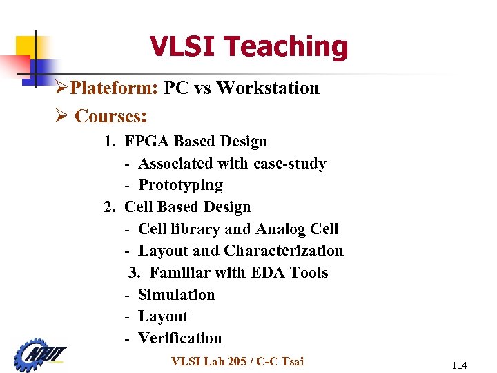 VLSI Teaching ØPlateform: PC vs Workstation Ø Courses: 1. FPGA Based Design - Associated with case-study - Prototyping 2. Cell Based Design - Cell library and Analog Cell - Layout and Characterization 3. Familiar with EDA Tools - Simulation - Layout - Verification VLSI Lab 205 / C-C Tsai 114
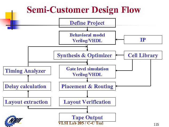 Semi-Customer Design Flow Define Project Behavioral model Verilog/VHDL Synthesis & Optimizer Timing Analyzer Placement & Routing Layout extraction Cell Library Gate level simulation Verilog/VHDL Delay calculation IP Layout Verification Tape Output VLSI Lab 205 / C-C Tsai 115
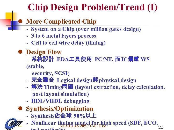 Chip Design Problem/Trend (I) l More Complicated Chip - System on a Chip (over million gates design) - 3 to 6 metal layers process - Cell to cell wire delay (timing) l Design Flow - 系統設計 EDA 具使用 PC/NT, 而 IC偏重 WS (stable, security, SCSI) - 完全整合 Logical design與 physical design - 解決 Timing問題 (layout extraction, delay calculation, post layout simulation) - HDL/VHDL debugging l Synthesis/Optimization - Synthesis佔全球 90%以上 - Nonlinear timing model. C-C Tsai speed (SDF, ECO, for high VLSI Lab 205 / 116
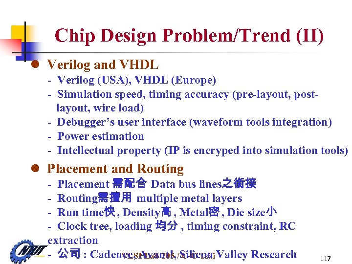 Chip Design Problem/Trend (II) l Verilog and VHDL - Verilog (USA), VHDL (Europe) - Simulation speed, timing accuracy (pre-layout, postlayout, wire load) - Debugger’s user interface (waveform tools integration) - Power estimation - Intellectual property (IP is encryped into simulation tools) l Placement and Routing - Placement 需配合 Data bus lines之銜接 - Routing需擅用 multiple metal layers - Run time快 , Density高 , Metal密 , Die size小 - Clock tree, loading 均分 , timing constraint, RC extraction - 公司 : Cadence, Avant!, /Silicon Valley Research VLSI Lab 205 C-C Tsai 117
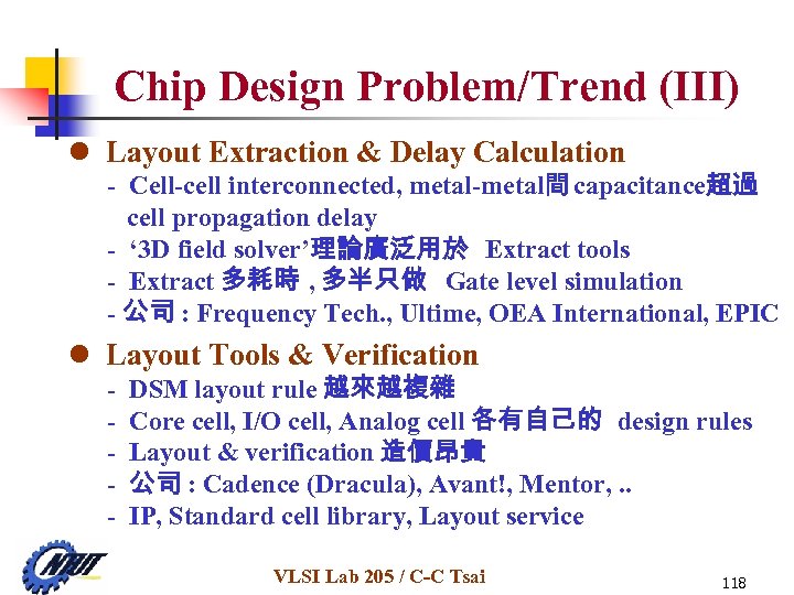 Chip Design Problem/Trend (III) l Layout Extraction & Delay Calculation - Cell-cell interconnected, metal-metal間 capacitance超過 cell propagation delay - ‘ 3 D field solver’理論廣泛用於 Extract tools - Extract 多耗時 , 多半只做 Gate level simulation - 公司 : Frequency Tech. , Ultime, OEA International, EPIC l Layout Tools & Verification - DSM layout rule 越來越複雜 Core cell, I/O cell, Analog cell 各有自己的 design rules Layout & verification 造價昂貴 公司 : Cadence (Dracula), Avant!, Mentor, . . IP, Standard cell library, Layout service VLSI Lab 205 / C-C Tsai 118
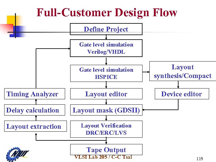 Full-Customer Design Flow Define Project Gate level simulation Verilog/VHDL Gate level simulation HSPICE Layout synthesis/Compact Timing Analyzer Layout editor Device editor Delay calculation Layout mask (GDSII) Layout extraction Layout Verification DRC/ERC/LVS Tape Output VLSI Lab 205 / C-C Tsai 119
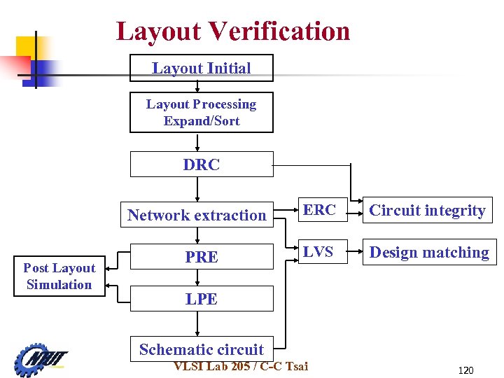 Layout Verification Layout Initial Layout Processing Expand/Sort DRC Network extraction Post Layout Simulation PRE ERC Circuit integrity LVS Design matching LPE Schematic circuit VLSI Lab 205 / C-C Tsai 120
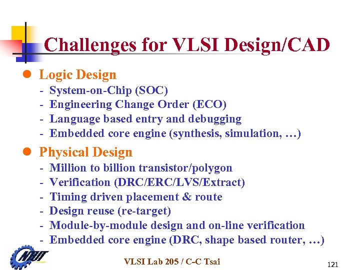 Challenges for VLSI Design/CAD l Logic Design - System-on-Chip (SOC) Engineering Change Order (ECO) Language based entry and debugging Embedded core engine (synthesis, simulation, …) l Physical Design - Million to billion transistor/polygon Verification (DRC/ERC/LVS/Extract) Timing driven placement & route Design reuse (re-target) Module-by-module design and on-line verification Embedded core engine (DRC, shape based router, …) VLSI Lab 205 / C-C Tsai 121
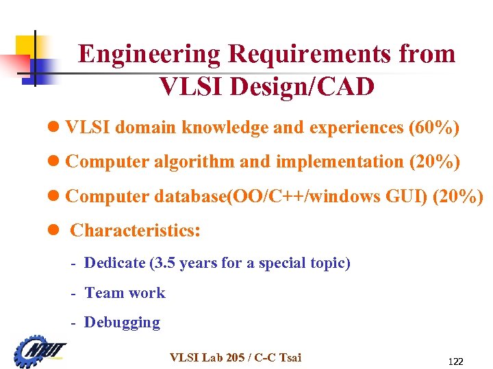 Engineering Requirements from VLSI Design/CAD l VLSI domain knowledge and experiences (60%) l Computer algorithm and implementation (20%) l Computer database(OO/C++/windows GUI) (20%) l Characteristics: - Dedicate (3. 5 years for a special topic) - Team work - Debugging VLSI Lab 205 / C-C Tsai 122
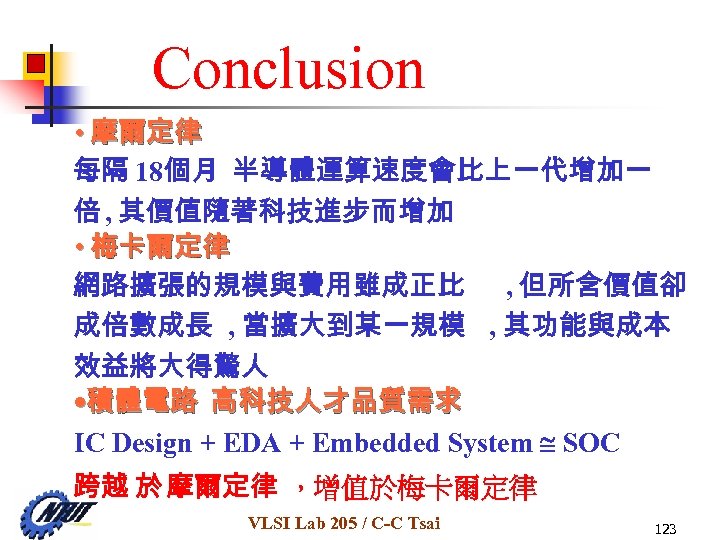 Conclusion • 摩爾定律 每隔 18個月 半導體運算速度會比上一代增加一 倍 , 其價值隨著科技進步而增加 • 梅卡爾定律 網路擴張的規模與費用雖成正比 , 但所含價值卻 成倍數成長 , 當擴大到某一規模 , 其功能與成本 效益將大得驚人 • 積體電路 高科技人才品質需求 IC Design + EDA + Embedded System SOC 跨越 於 摩爾定律 ,增值於梅卡爾定律 VLSI Lab 205 / C-C Tsai 123


