91cf18cb9b3c4637a151eec1e61bb832.ppt
- Количество слайдов: 44
 VLSI/FPGA Design and Test CAD Tool Flow in Mentor Graphics (Automating the Concept-to-ASIC Design Process) Victor P. Nelson Feb 15, 2006 VLSI D&T Seminar 1
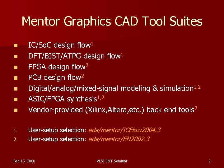 Mentor Graphics CAD Tool Suites n n n n 1. 2. IC/So. C design flow 1 DFT/BIST/ATPG design flow 1 FPGA design flow 2 PCB design flow 2 Digital/analog/mixed-signal modeling & simulation 1, 2 ASIC/FPGA synthesis 1, 2 Vendor-provided (Xilinx, Altera, etc. ) back end tools 2 User-setup selection: eda/mentor/ICFlow 2004. 3 User-setup selection: eda/mentor/EN 2002. 3 Feb 15, 2006 VLSI D&T Seminar 2
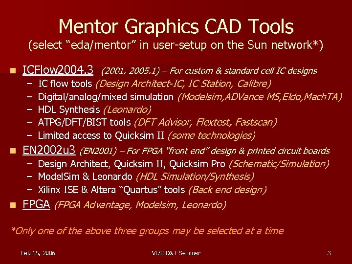 Mentor Graphics CAD Tools (select “eda/mentor” in user-setup on the Sun network*) n ICFlow 2004. 3 – – – n (2001, 2005. 1) – For custom & standard cell IC designs IC flow tools (Design Architect-IC, IC Station, Calibre) Digital/analog/mixed simulation (Modelsim, ADVance MS, Eldo, Mach. TA) HDL Synthesis (Leonardo) ATPG/DFT/BIST tools (DFT Advisor, Flextest, Fastscan) Limited access to Quicksim II (some technologies) EN 2002 u 3 (EN 2001) – For FPGA “front end” design & printed circuit boards – Design Architect, Quicksim II, Quicksim Pro (Schematic/Simulation) – Model. Sim & Leonardo (HDL Simulation/Synthesis) – Xilinx ISE & Altera “Quartus” tools (Back end design) n FPGA (FPGA Advantage, Modelsim, Leonardo) *Only one of the above three groups may be selected at a time Feb 15, 2006 VLSI D&T Seminar 3
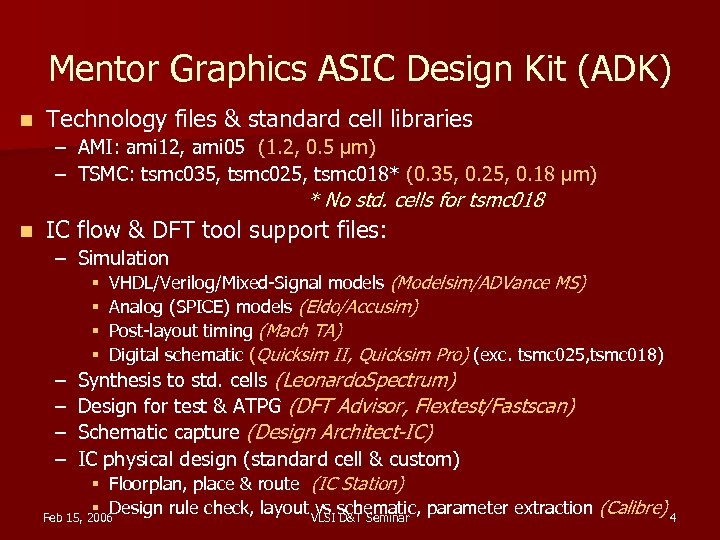 Mentor Graphics ASIC Design Kit (ADK) n Technology files & standard cell libraries – AMI: ami 12, ami 05 (1. 2, 0. 5 μm) – TSMC: tsmc 035, tsmc 025, tsmc 018* (0. 35, 0. 25, 0. 18 μm) * No std. cells for tsmc 018 n IC flow & DFT tool support files: – Simulation § § – – VHDL/Verilog/Mixed-Signal models (Modelsim/ADVance MS) Analog (SPICE) models (Eldo/Accusim) Post-layout timing (Mach TA) Digital schematic (Quicksim II, Quicksim Pro) (exc. tsmc 025, tsmc 018) Synthesis to std. cells (Leonardo. Spectrum) Design for test & ATPG (DFT Advisor, Flextest/Fastscan) Schematic capture (Design Architect-IC) IC physical design (standard cell & custom) § Floorplan, place & route (IC Station) § Design rule check, layout VLSI schematic, parameter extraction (Calibre) 4 vs D&T Seminar Feb 15, 2006
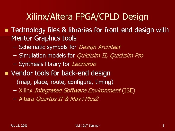 Xilinx/Altera FPGA/CPLD Design n Technology files & libraries for front-end design with Mentor Graphics tools – – – n Schematic symbols for Design Architect Simulation models for Quicksim II, Quicksim Pro Synthesis library for Leonardo Vendor tools for back-end design (map, place, route, configure, timing) – Xilinx Integrated Software Environment (ISE) – Altera Quartus II & Max+Plus 2 Feb 15, 2006 VLSI D&T Seminar 5
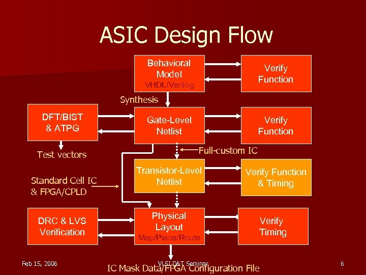 ASIC Design Flow Behavioral Model Verify Function VHDL/Verilog Synthesis DFT/BIST & ATPG Gate-Level Netlist Full-custom IC Test vectors Standard Cell IC & FPGA/CPLD DRC & LVS Verification Feb 15, 2006 Verify Function Transistor-Level Netlist Physical Layout Map/Place/Route VLSI D&T Seminar Verify Function & Timing Verify Timing IC Mask Data/FPGA Configuration File 6
 Digital/Mixed-Signal Simulation VHDL, Verilog, VHDL-AMS, Verilog-A, SPICE Models Working Library Simulation Setup Eldo, Eldo RF Analog (SPICE) Feb 15, 2006 Mach TA Design_1 Design_2 Resource Libraries VITAL IEEE 1164 ADVance MS EZwave or Xelga View Results VLSI D&T Seminar Input Stimuli Model. Sim Digital (VHDL, Verilog) Mixed Signal (VHDL-AMS, Verilog-A) 7
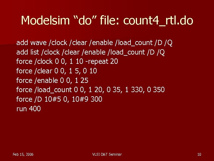
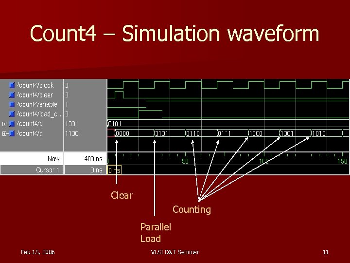
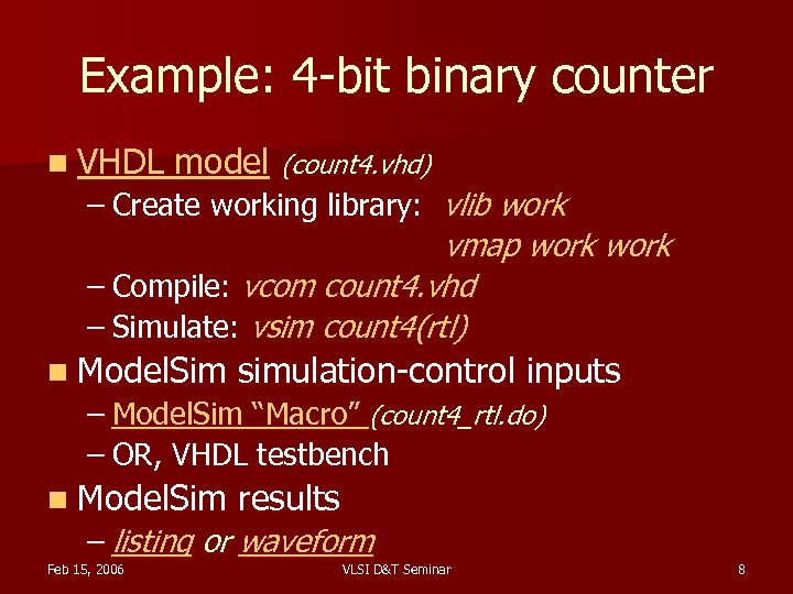 Example: 4 -bit binary counter n VHDL model (count 4. vhd) – Create working library: vlib work vmap work – Compile: vcom count 4. vhd – Simulate: vsim count 4(rtl) n Model. Sim simulation-control inputs – Model. Sim “Macro” (count 4_rtl. do) – OR, VHDL testbench n Model. Sim results – listing or waveform Feb 15, 2006 VLSI D&T Seminar 8
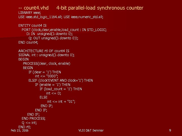 -- count 4. vhd 4 -bit parallel-load synchronous counter LIBRARY ieee; USE ieee. std_logic_1164. all; USE ieee. numeric_std. all; ENTITY count 4 IS PORT (clock, clear, enable, load_count : IN STD_LOGIC; D: IN unsigned(3 downto 0); Q: OUT unsigned(3 downto 0)); END count 4; ARCHITECTURE rtl OF count 4 IS SIGNAL int : unsigned(3 downto 0); BEGIN PROCESS(clear, clock, enable) BEGIN IF (clear = '1') THEN int <= "0000"; ELSIF (clock'EVENT AND clock='1') THEN IF (enable = '1') THEN IF (load_count = '1') THEN int <= D; ELSE int <= int + "01"; END IF; END PROCESS; Q <= int; END rtl; Feb 15, 2006 VLSI D&T Seminar 9
 Modelsim “do” file: count 4_rtl. do add wave /clock /clear /enable /load_count /D /Q add list /clock /clear /enable /load_count /D /Q force /clock 0 0, 1 10 -repeat 20 force /clear 0 0, 1 5, 0 10 force /enable 0 0, 1 25 force /load_count 0 0, 1 20, 0 35, 1 330, 0 350 force /D 10#5 0, 10#9 300 run 400 Feb 15, 2006 VLSI D&T Seminar 10
 Count 4 – Simulation waveform Clear Counting Parallel Load Feb 15, 2006 VLSI D&T Seminar 11
 Automated Synthesis with Leonardo Spectrum Technology Synthesis Libraries FPGA VHDL/Verilog Behavioral/RTL Models Leonardo Spectrum (Level 3) Design Constraints ASIC ADK AMI 0. 5, 1. 2 TSMC 0. 35, 0. 25 Feb 15, 2006 Technology. Specific Netlist VHDL, Verilog, SDF, EDIF, XNF VLSI D&T Seminar Level 1 – FPGA Level 2 – FPGA + Timing 12
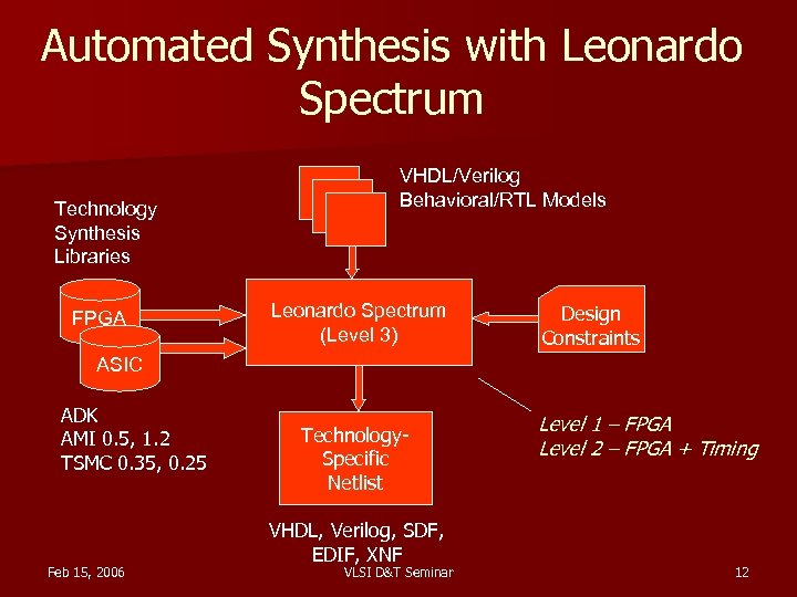
 Synthesis in Leonardo: HDL to technology-specific netlist Invoke leonardo 2. Select & load a technology library (ASIC or FPGA) 1. – ASIC > ADK > TSMC 0. 35 micron Read input VHDL/Verilog file(s): count 4. vhd 4. Enter any constraints (clock freq, delays, etc. ) 5. Optimize for area/delay/effort level 6. Write output file(s) 3. – count 4_0. vhd - VHDL netlist – count 4. v - Verilog netlist (for IC layout) – count 4. sdf - Standard delay format file (for timing) Feb 15, 2006 VLSI D&T Seminar 13 – count 4. edf - EDIF netlist (for Xilinx/Altera FPGA)
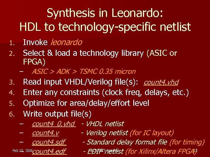
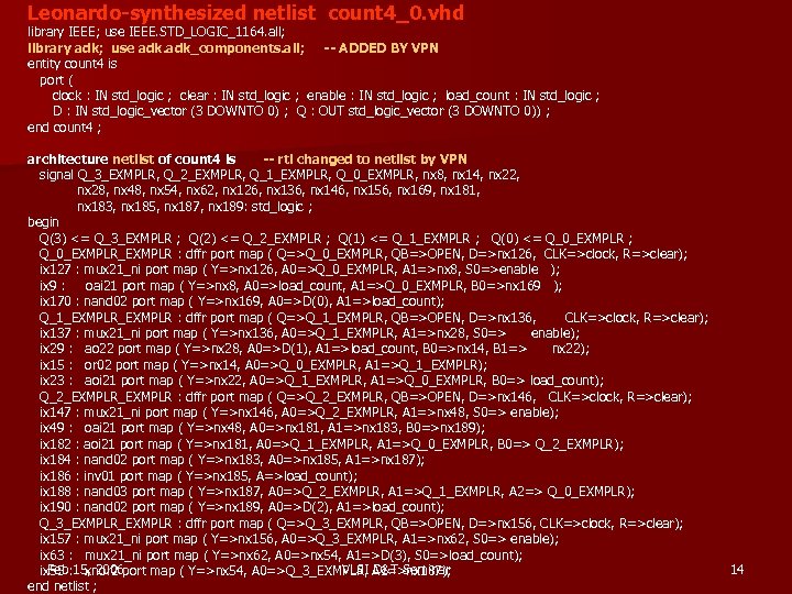 Leonardo-synthesized netlist count 4_0. vhd library IEEE; use IEEE. STD_LOGIC_1164. all; library adk; use adk_components. all; -- ADDED BY VPN entity count 4 is port ( clock : IN std_logic ; clear : IN std_logic ; enable : IN std_logic ; load_count : IN std_logic ; D : IN std_logic_vector (3 DOWNTO 0) ; Q : OUT std_logic_vector (3 DOWNTO 0)) ; end count 4 ; architecture netlist of count 4 is -- rtl changed to netlist by VPN signal Q_3_EXMPLR, Q_2_EXMPLR, Q_1_EXMPLR, Q_0_EXMPLR, nx 8, nx 14, nx 22, nx 28, nx 48, nx 54, nx 62, nx 126, nx 136, nx 146, nx 156, nx 169, nx 181, nx 183, nx 185, nx 187, nx 189: std_logic ; begin Q(3) <= Q_3_EXMPLR ; Q(2) <= Q_2_EXMPLR ; Q(1) <= Q_1_EXMPLR ; Q(0) <= Q_0_EXMPLR ; Q_0_EXMPLR : dffr port map ( Q=>Q_0_EXMPLR, QB=>OPEN, D=>nx 126, CLK=>clock, R=>clear); ix 127 : mux 21_ni port map ( Y=>nx 126, A 0=>Q_0_EXMPLR, A 1=>nx 8, S 0=>enable ); ix 9 : oai 21 port map ( Y=>nx 8, A 0=>load_count, A 1=>Q_0_EXMPLR, B 0=>nx 169 ); ix 170 : nand 02 port map ( Y=>nx 169, A 0=>D(0), A 1=>load_count); Q_1_EXMPLR : dffr port map ( Q=>Q_1_EXMPLR, QB=>OPEN, D=>nx 136, CLK=>clock, R=>clear); ix 137 : mux 21_ni port map ( Y=>nx 136, A 0=>Q_1_EXMPLR, A 1=>nx 28, S 0=> enable); ix 29 : ao 22 port map ( Y=>nx 28, A 0=>D(1), A 1=>load_count, B 0=>nx 14, B 1=> nx 22); ix 15 : or 02 port map ( Y=>nx 14, A 0=>Q_0_EXMPLR, A 1=>Q_1_EXMPLR); ix 23 : aoi 21 port map ( Y=>nx 22, A 0=>Q_1_EXMPLR, A 1=>Q_0_EXMPLR, B 0=> load_count); Q_2_EXMPLR : dffr port map ( Q=>Q_2_EXMPLR, QB=>OPEN, D=>nx 146, CLK=>clock, R=>clear); ix 147 : mux 21_ni port map ( Y=>nx 146, A 0=>Q_2_EXMPLR, A 1=>nx 48, S 0=> enable); ix 49 : oai 21 port map ( Y=>nx 48, A 0=>nx 181, A 1=>nx 183, B 0=>nx 189); ix 182 : aoi 21 port map ( Y=>nx 181, A 0=>Q_1_EXMPLR, A 1=>Q_0_EXMPLR, B 0=> Q_2_EXMPLR); ix 184 : nand 02 port map ( Y=>nx 183, A 0=>nx 185, A 1=>nx 187); ix 186 : inv 01 port map ( Y=>nx 185, A=>load_count); ix 188 : nand 03 port map ( Y=>nx 187, A 0=>Q_2_EXMPLR, A 1=>Q_1_EXMPLR, A 2=> Q_0_EXMPLR); ix 190 : nand 02 port map ( Y=>nx 189, A 0=>D(2), A 1=>load_count); Q_3_EXMPLR : dffr port map ( Q=>Q_3_EXMPLR, QB=>OPEN, D=>nx 156, CLK=>clock, R=>clear); ix 157 : mux 21_ni port map ( Y=>nx 156, A 0=>Q_3_EXMPLR, A 1=>nx 62, S 0=> enable); ix 63 : mux 21_ni port map ( Y=>nx 62, A 0=>nx 54, A 1=>D(3), S 0=> load_count); Feb xnor 2 VLSI D&T Seminar ix 55 : 15, 2006 port map ( Y=>nx 54, A 0=>Q_3_EXMPLR, A 1=>nx 187); end netlist ; 14
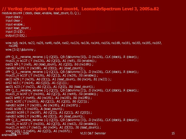 // Verilog description for cell count 4, Leonardo. Spectrum Level 3, 2005 a. 82 module count 4 ( clock, clear, enable, load_count, D, Q ) ; input clock ; input clear ; input enable ; input load_count ; input [3: 0]D ; output [3: 0]Q ; wire nx 8, nx 14, nx 22, nx 28, nx 48, nx 54, nx 62, nx 126, nx 136, nx 146, nx 156, nx 169, nx 181, nx 183, nx 185, nx 187, nx 189; wire [3: 0] $dummy ; dffr Q_0__rename (. Q (Q[0]), . QB ($dummy [0]), . D (nx 126), . CLK (clock), . R (clear)) ; mux 21_ni ix 127 (. Y (nx 126), . A 0 (Q[0]), . A 1 (nx 8), . S 0 (enable)) ; oai 21 ix 9 (. Y (nx 8), . A 0 (load_count), . A 1 (Q[0]), . B 0 (nx 169)) ; nand 02 ix 170 (. Y (nx 169), . A 0 (D[0]), . A 1 (load_count)) ; dffr Q_1__rename (. Q (Q[1]), . QB ($dummy [1]), . D (nx 136), . CLK (clock), . R (clear)) ; mux 21_ni ix 137 (. Y (nx 136), . A 0 (Q[1]), . A 1 (nx 28), . S 0 (enable)) ; ao 22 ix 29 (. Y (nx 28), . A 0 (D[1]), . A 1 (load_count), . B 0 (nx 14), . B 1 (nx 22) ) ; or 02 ix 15 (. Y (nx 14), . A 0 (Q[0]), . A 1 (Q[1])) ; aoi 21 ix 23 (. Y (nx 22), . A 0 (Q[1]), . A 1 (Q[0]), . B 0 ( load_count)) ; dffr Q_2__rename (. Q (Q[2]), . QB ($dummy [2]), . D (nx 146), . CLK (clock), . R (clear)) ; mux 21_ni ix 147 (. Y (nx 146), . A 0 (Q[2]), . A 1 (nx 48), . S 0 (enable)) ; oai 21 ix 49 (. Y (nx 48), . A 0 (nx 181), . A 1 (nx 183), . B 0 (nx 189)) ; aoi 21 ix 182 (. Y (nx 181), . A 0 (Q[1]), . A 1 (Q[0]), . B 0 (Q[2])) ; nand 02 ix 184 (. Y (nx 183), . A 0 (nx 185), . A 1 (nx 187)) ; inv 01 ix 186 (. Y (nx 185), . A (load_count)) ; nand 03 ix 188 (. Y (nx 187), . A 0 (Q[2]), . A 1 (Q[1]), . A 2 (Q[0])) ; nand 02 ix 190 (. Y (nx 189), . A 0 (D[2]), . A 1 (load_count)) ; dffr Q_3__rename (. Q (Q[3]), . QB ($dummy [3]), . D (nx 156), . CLK (clock), . R (clear)) ; mux 21_ni ix 157 (. Y (nx 156), . A 0 (Q[3]), . A 1 (nx 62), . S 0 (enable)) ; mux 21_ni ix 63 (. Y (nx 62), . A 0 (nx 54), . A 1 (D[3]), . S 0 ( load_count)) ; xnor 2 ix 55 (. Y (nx 54), . A 0 (Q[3]), . A 1 (nx 187)) ; Feb VLSI D&T Seminar endmodule 15, 2006 15
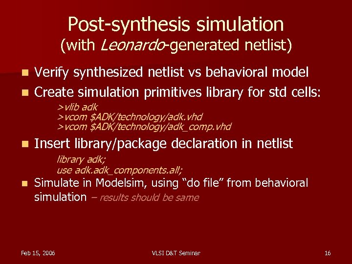 Post-synthesis simulation (with Leonardo-generated netlist) Verify synthesized netlist vs behavioral model n Create simulation primitives library for std cells: n >vlib adk >vcom $ADK/technology/adk. vhd >vcom $ADK/technology/adk_comp. vhd n Insert library/package declaration in netlist library adk; use adk_components. all; n Simulate in Modelsim, using “do file” from behavioral simulation – results should be same Feb 15, 2006 VLSI D&T Seminar 16
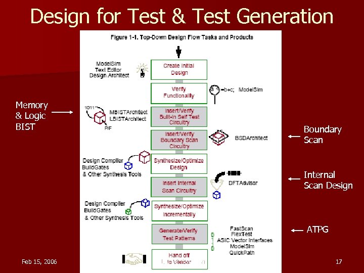 Design for Test & Test Generation Memory & Logic BIST Boundary Scan Internal Scan Design ATPG Feb 15, 2006 VLSI D&T Seminar 17
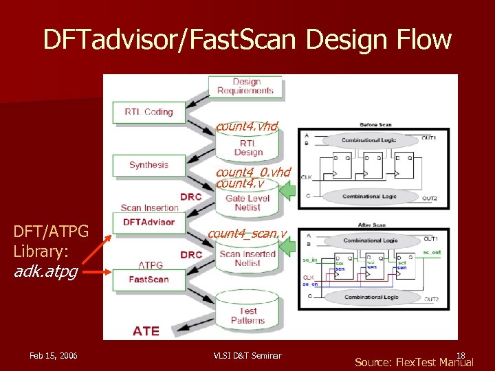 DFTadvisor/Fast. Scan Design Flow count 4. vhd count 4_0. vhd count 4. v DFT/ATPG Library: count 4_scan. v adk. atpg Feb 15, 2006 VLSI D&T Seminar 18 Source: Flex. Test Manual
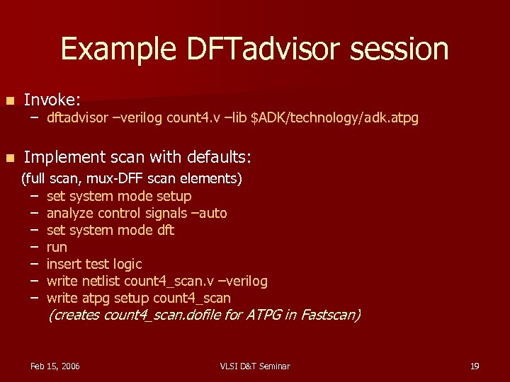 Example DFTadvisor session n Invoke: n Implement scan with defaults: – dftadvisor –verilog count 4. v –lib $ADK/technology/adk. atpg (full scan, mux-DFF scan elements) – set system mode setup – analyze control signals –auto – set system mode dft – run – insert test logic – write netlist count 4_scan. v –verilog – write atpg setup count 4_scan (creates count 4_scan. dofile for ATPG in Fastscan) Feb 15, 2006 VLSI D&T Seminar 19
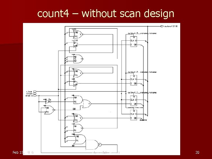 count 4 – without scan design Feb 15, 2006 VLSI D&T Seminar 20
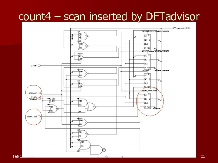 count 4 – scan inserted by DFTadvisor Feb 15, 2006 VLSI D&T Seminar 21
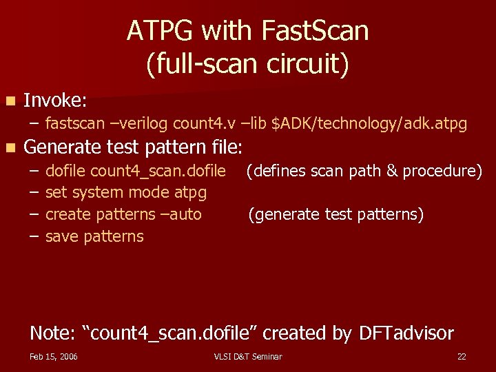 ATPG with Fast. Scan (full-scan circuit) n Invoke: – fastscan –verilog count 4. v –lib $ADK/technology/adk. atpg n Generate test pattern file: – – dofile count 4_scan. dofile set system mode atpg create patterns –auto save patterns (defines scan path & procedure) (generate test patterns) Note: “count 4_scan. dofile” created by DFTadvisor Feb 15, 2006 VLSI D&T Seminar 22
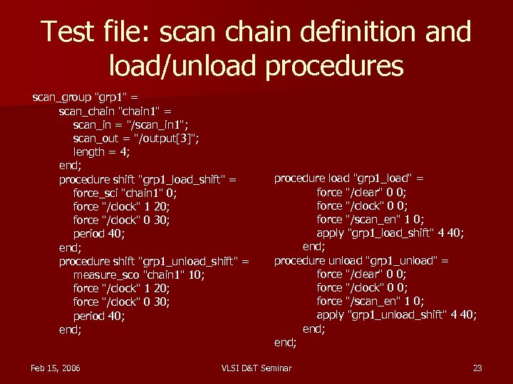 Test file: scan chain definition and load/unload procedures scan_group "grp 1" = scan_chain "chain 1" = scan_in = "/scan_in 1"; scan_out = "/output[3]"; length = 4; end; procedure shift "grp 1_load_shift" = force_sci "chain 1" 0; force "/clock" 1 20; force "/clock" 0 30; period 40; end; procedure shift "grp 1_unload_shift" = measure_sco "chain 1" 10; force "/clock" 1 20; force "/clock" 0 30; period 40; end; Feb 15, 2006 procedure load "grp 1_load" = force "/clear" 0 0; force "/clock" 0 0; force "/scan_en" 1 0; apply "grp 1_load_shift" 4 40; end; procedure unload "grp 1_unload" = force "/clear" 0 0; force "/clock" 0 0; force "/scan_en" 1 0; apply "grp 1_unload_shift" 4 40; end; VLSI D&T Seminar 23
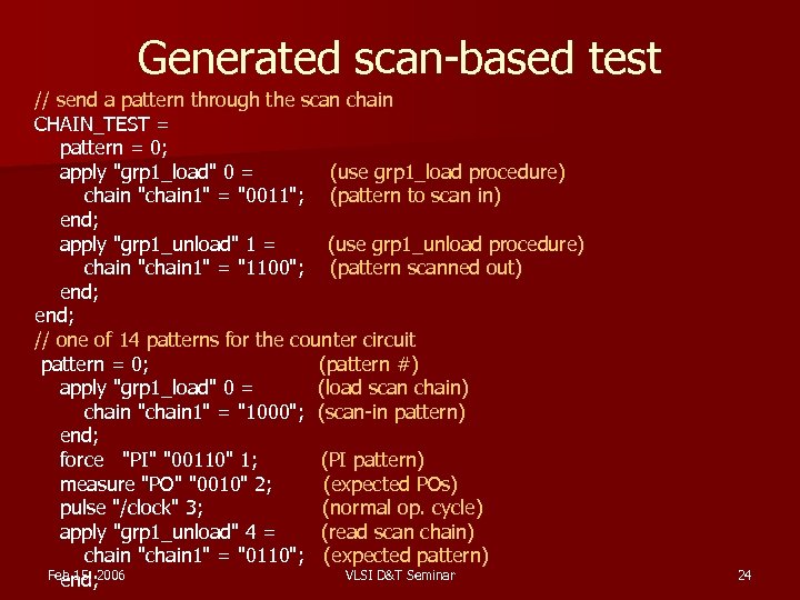 Generated scan-based test // send a pattern through the scan chain CHAIN_TEST = pattern = 0; apply "grp 1_load" 0 = (use grp 1_load procedure) chain "chain 1" = "0011"; (pattern to scan in) end; apply "grp 1_unload" 1 = (use grp 1_unload procedure) chain "chain 1" = "1100"; (pattern scanned out) end; // one of 14 patterns for the counter circuit pattern = 0; (pattern #) apply "grp 1_load" 0 = (load scan chain) chain "chain 1" = "1000"; (scan-in pattern) end; force "PI" "00110" 1; (PI pattern) measure "PO" "0010" 2; (expected POs) pulse "/clock" 3; (normal op. cycle) apply "grp 1_unload" 4 = (read scan chain) chain "chain 1" = "0110"; (expected pattern) Feb 15, 2006 VLSI D&T Seminar end; 24
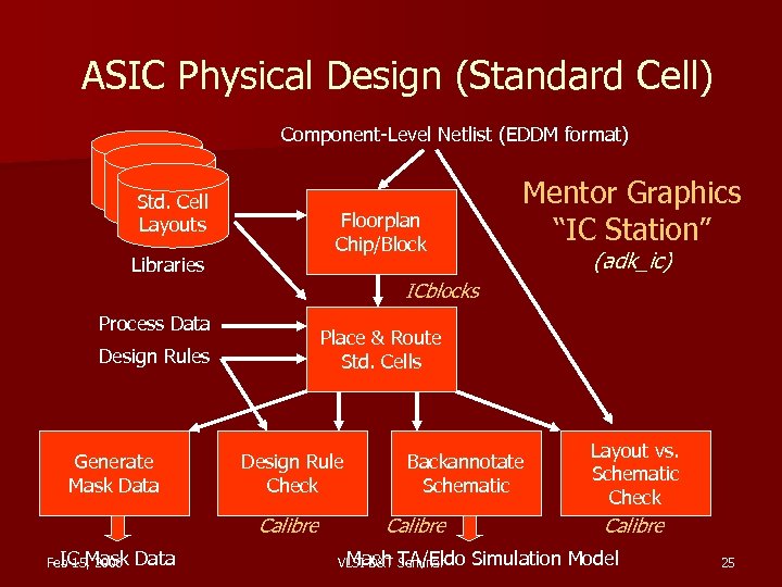 ASIC Physical Design (Standard Cell) Component-Level Netlist (EDDM format) Std. Cell Layouts Mentor Graphics “IC Station” Floorplan Chip/Block Libraries (adk_ic) ICblocks Process Data Place & Route Std. Cells Design Rules Generate Mask Data Design Rule Check Calibre IC Mask Feb 15, 2006 Data Backannotate Schematic Calibre Mach TA/Eldo VLSI D&T Seminar Layout vs. Schematic Check Calibre Simulation Model 25
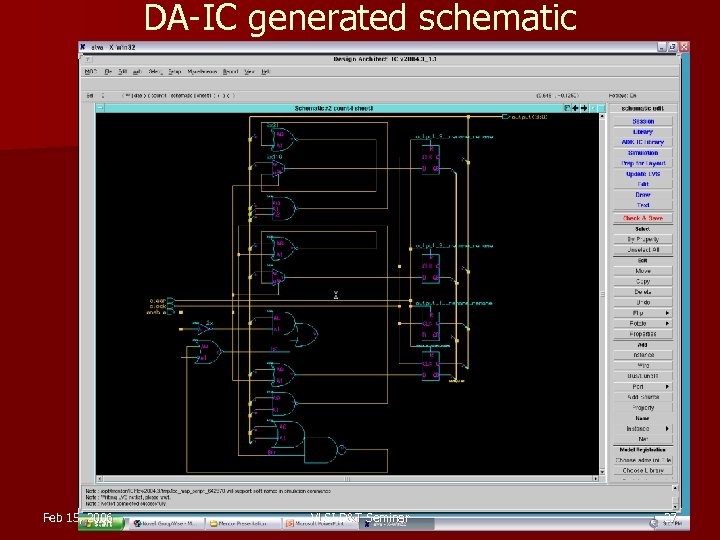
 Preparation for Layout 1. Use Design Architect-IC to convert Verilog netlist to Mentor Graphics “EDDM” schematic/netlist format – – 2. 3. n Invoke Design Architect-IC (adk_daic) On menu bar, select File > Import Verilog § Netlist file: count 4. v (the Verilog netlist) § Output directory: count 4 (for the EDDM netlist) § Mapping file $ADK/technology/adk_map. vmp Open the generated schematic for viewing – – – Click Schematic in DA-IC palette Select schematic in directory named above (see next slide) Click Update LVS in the schematic palette to create a netlist to be used later by “Calibre” Create design viewpoints for ICstation tools – adk_dve count 4 –t tsmc 035 (V. P’s: layout, lvs, sdl, tsmc 035) Can also create gate/transistor schematics directly in DAIC using components from the ADK library Feb 15, 2006 VLSI D&T Seminar 26
 DA-IC generated schematic Feb 15, 2006 VLSI D&T Seminar 27
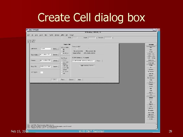
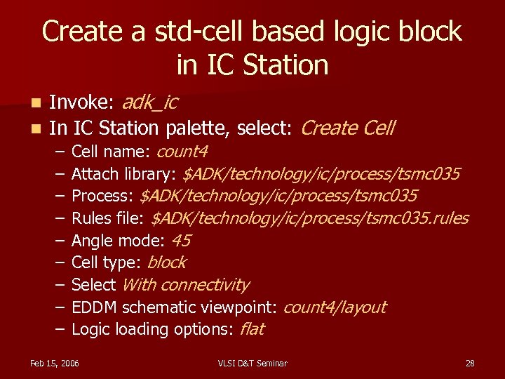 Create a std-cell based logic block in IC Station Invoke: adk_ic n In IC Station palette, select: Create Cell n – – – – – Cell name: count 4 Attach library: $ADK/technology/ic/process/tsmc 035 Process: $ADK/technology/ic/process/tsmc 035 Rules file: $ADK/technology/ic/process/tsmc 035. rules Angle mode: 45 Cell type: block Select With connectivity EDDM schematic viewpoint: count 4/layout Logic loading options: flat Feb 15, 2006 VLSI D&T Seminar 28
 Create Cell dialog box Feb 15, 2006 VLSI D&T Seminar 29
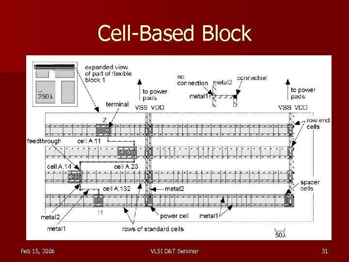
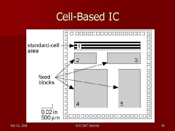 Cell-Based IC Feb 15, 2006 VLSI D&T Seminar 30
 Cell-Based Block Feb 15, 2006 VLSI D&T Seminar 31
 Basic standard Cell layout Feb 15, 2006 VLSI D&T Seminar. Source: Weste “CMOS VLSI Design” 32
 Auto “floorplan” the block place & route > autofp Feb 15, 2006 VLSI D&T Seminar 33
 Auto-place the std cells Autoplc > Std. Cel Feb 15, 2006 VLSI D&T Seminar 34
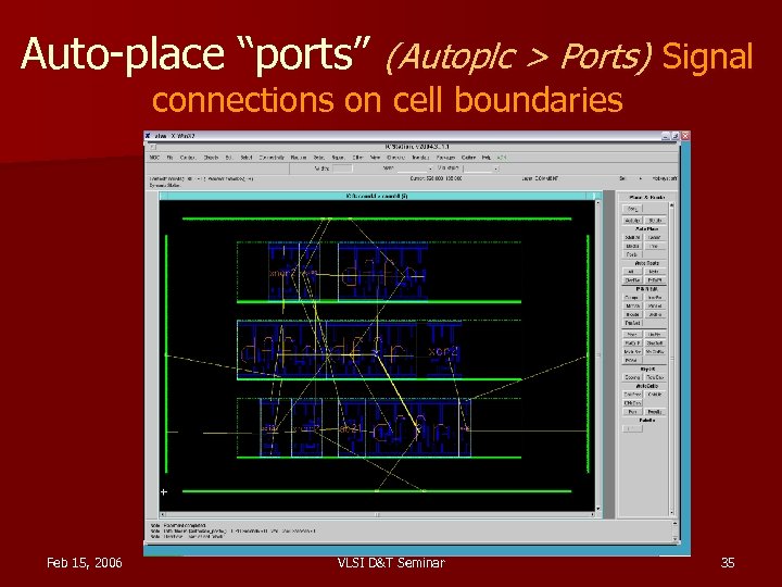 Auto-place “ports” (Autoplc > Ports) Signal connections on cell boundaries Feb 15, 2006 VLSI D&T Seminar 35
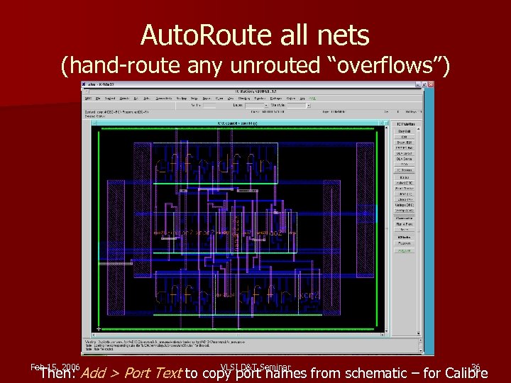 Auto. Route all nets (hand-route any unrouted “overflows”) Feb 15, 2006 VLSI D&T Seminar 36 Then: Add > Port Text to copy port names from schematic – for Calibre
 Layout design rule check (DRC) n Technology-specific design rules specify minimum sizes, spacing, etc. of features to ensure reliable fabrication – Design rules file specified at startup Ex. tsmc 035. rules n From main palette, select ICrules – Click Check and then OK in prompt box (can optionally select a specific area to check) – Rules checked in numeric order Feb 15, 2006 VLSI D&T Seminar 37
 Common errors detected by DRC n To fix, click on First in palette to highlight first error – – n Error is highlighted in the layout Click View to zoom in to the error (see next) Example: DRC 9_2: Metal 2 spacing = 3 L Fix by drawing a rectangle of metal 2 to fill in the gap between contacts that should be connected Click Next to go to next error, until all are fixed NOTE: There must be no DRC errors if MOSIS is to fabricate the chip – they will run their own DRC. Feb 15, 2006 VLSI D&T Seminar 38
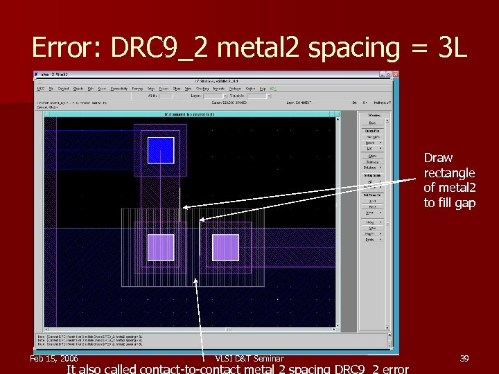 Error: DRC 9_2 metal 2 spacing = 3 L Draw rectangle of metal 2 to fill gap Feb 15, 2006 VLSI D&T Seminar 39
 Layout vs schematic check Calibre Interactive LVS n From ICstation menu: Calibre > Run LVS – – – n In popup, Calibre location: $MGC_HOME/. . /Calibre Rules: $ADK/technology/ic/process/tsmc 035. calibre. rules Input: count 4. src. net (previously created in DA-IC) H-cells: $ADK/technology/adk. hcell (hierarchical cells) Extracted file: count 4. lay. net Compares extracted transistor-level netlist vs. netlist saved in DA-IC Feb 15, 2006 VLSI D&T Seminar 40
 Post-layout parameter extraction Calibre Interactive PEX n Extract Spice netlist, including parasitic RC – Simulate in Eldo or Mach. TA n ICstation menu: Calibre>Run PEX – Options similar to Calibre LVS – Extraction options: § lumped C + coupling cap’s § distributed RC + coupling cap’s – Output file: count 4. pex. netlist Feb 15, 2006 VLSI D&T Seminar 41
 Post-layout simulation with Mach. TA n Mach. TA is an accelerated Spice simulator – – – n Can do standard Spice analyses (dc transient) Can execute a test vector file Results displayed in “EZwave” Prepare netlist for Mach. TA (remove subcircuits) – mta_prep count 4 n Invoke: mta –ezw –t $ADK/technology/mta/tsmc 035 TYP count 4. sp Feb 15, 2006 VLSI D&T Seminar 42
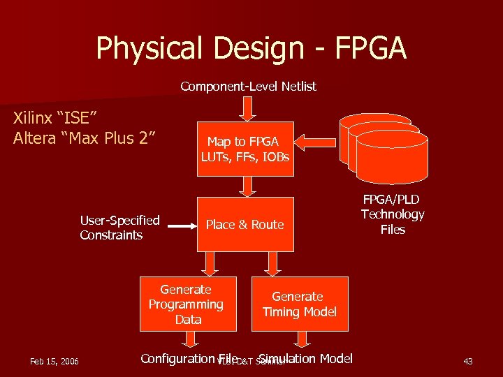 Physical Design - FPGA Component-Level Netlist Xilinx “ISE” Altera “Max Plus 2” User-Specified Constraints Map to FPGA LUTs, FFs, IOBs Place & Route Generate Programming Data Feb 15, 2006 FPGA/PLD Technology Files Generate Timing Model Configuration VLSI D&T Seminar File Simulation Model 43
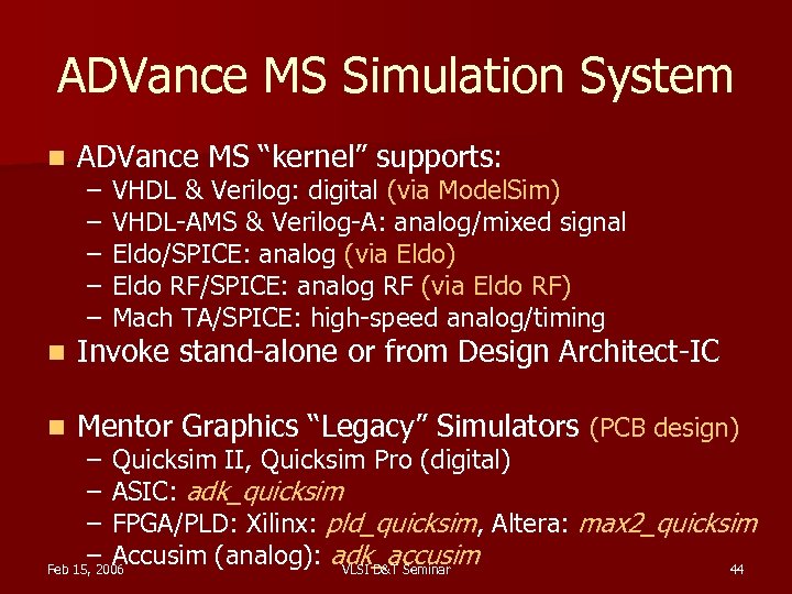 ADVance MS Simulation System n ADVance MS “kernel” supports: n Invoke stand-alone or from Design Architect-IC n Mentor Graphics “Legacy” Simulators (PCB design) – – – VHDL & Verilog: digital (via Model. Sim) VHDL-AMS & Verilog-A: analog/mixed signal Eldo/SPICE: analog (via Eldo) Eldo RF/SPICE: analog RF (via Eldo RF) Mach TA/SPICE: high-speed analog/timing – Quicksim II, Quicksim Pro (digital) – ASIC: adk_quicksim – FPGA/PLD: Xilinx: pld_quicksim, Altera: max 2_quicksim – Accusim (analog): adk_accusim Feb 15, 2006 VLSI D&T Seminar 44


