f420477b8e2ec910e35acdb281cf68e4.ppt
- Количество слайдов: 107
 VLSI Design Chapter 5 CMOS Circuit and Logic Design Jin-Fu Li
 Chapter 5 CMOS Circuit and Logic Design • • • CMOS Logic Gate Design Physical Design of Logic Gates CMOS Logic Structures Clocking Strategies I/O Structures Low-Power Design National Central University EE 613 VLSI Design 2
 Logic Gate Design Issues • Hierarchical design - Architecture level - RTL/logic gate level - Circuit level - Layout level • Critical paths – the path with the longest delay that require attention to timing details • The number of Fanins and Fanouts affects the performance of the circuits National Central University EE 613 VLSI Design 3
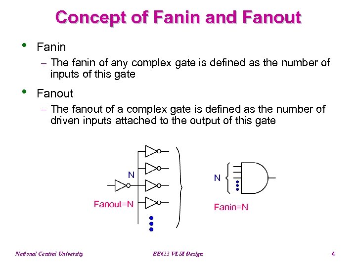 Concept of Fanin and Fanout • Fanin - The fanin of any complex gate is defined as the number of inputs of this gate • Fanout - The fanout of a complex gate is defined as the number of driven inputs attached to the output of this gate N N Fanout=N National Central University Fanin=N EE 613 VLSI Design 4
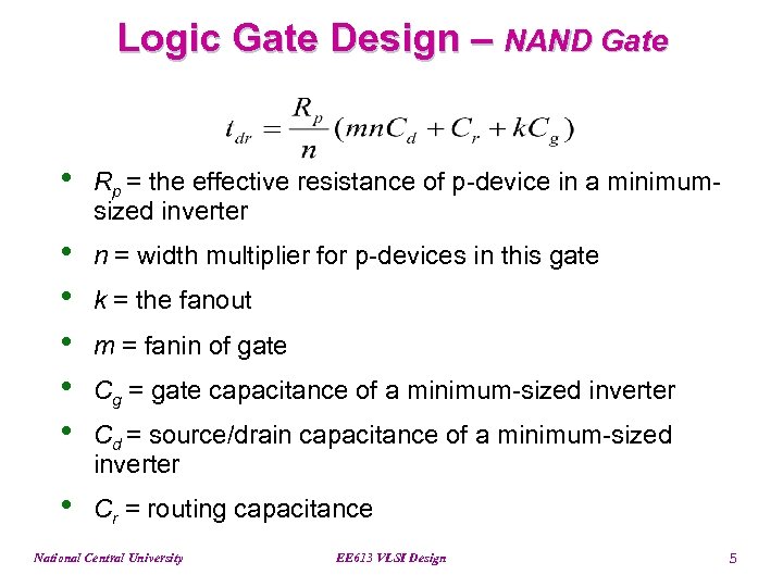 Logic Gate Design – NAND Gate • Rp = the effective resistance of p-device in a minimumsized inverter • • • n = width multiplier for p-devices in this gate • Cr = routing capacitance k = the fanout m = fanin of gate Cg = gate capacitance of a minimum-sized inverter Cd = source/drain capacitance of a minimum-sized inverter National Central University EE 613 VLSI Design 5
 Logic Gate Design – Fanins and Fanouts National Central University EE 613 VLSI Design 6
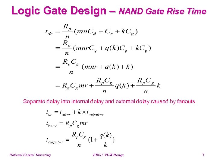 Logic Gate Design – NAND Gate Rise Time Separate delay into internal delay and external delay caused by fanouts National Central University EE 613 VLSI Design 7
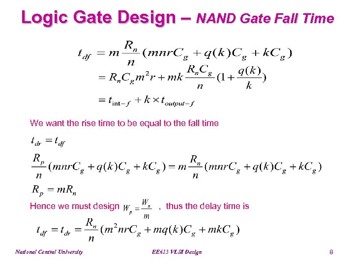 Logic Gate Design – NAND Gate Fall Time We want the rise time to be equal to the fall time Hence we must design National Central University , thus the delay time is EE 613 VLSI Design 8
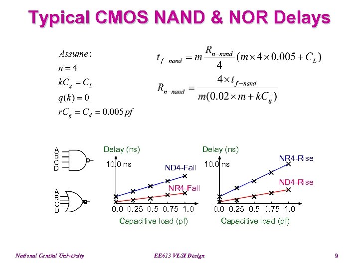 Typical CMOS NAND & NOR Delays A B C D National Central University Delay (ns) 10. 0 ns ND 4 -Fall 10. 0 ns NR 4 -Fall 0. 0 0. 25 0. 75 1. 0 Capacitive load (pf) EE 613 VLSI Design NR 4 -Rise ND 4 -Rise 0. 0 0. 25 0. 75 1. 0 Capacitive load (pf) 9
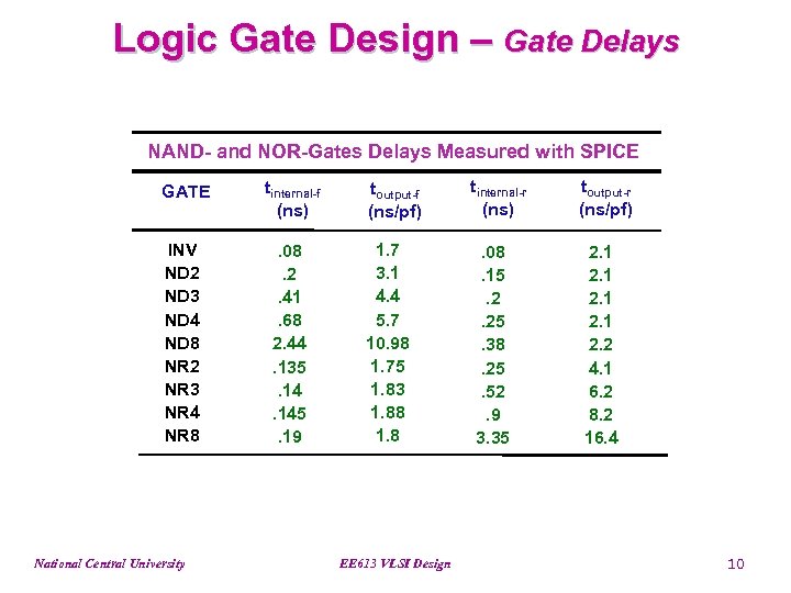 Logic Gate Design – Gate Delays NAND- and NOR-Gates Delays Measured with SPICE GATE tinternal-f (ns) INV ND 2 ND 3 ND 4 ND 8 NR 2 NR 3 NR 4 NR 8 . 08. 2. 41. 68 2. 44. 135. 145. 19 National Central University toutput-f (ns/pf) 1. 7 3. 1 4. 4 5. 7 10. 98 1. 75 1. 83 1. 88 1. 8 EE 613 VLSI Design tinternal-r (ns). 08. 15. 2. 25. 38. 25. 52. 9 3. 35 toutput-r (ns/pf) 2. 1 2. 2 4. 1 6. 2 8. 2 16. 4 10
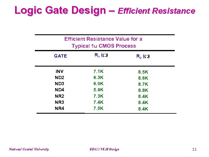 Logic Gate Design – Efficient Resistance Value for a Typical 1 u CMOS Process GATE INV ND 2 ND 3 ND 4 NR 2 NR 3 NR 4 National Central University Rn ( ) 7. 1 K 6. 3 K 6. 0 K 5. 9 K 7. 3 K 7. 4 K 7. 5 K EE 613 VLSI Design Rp ( ) 8. 5 K 8. 6 K 8. 7 K 8. 8 K 8. 4 K 11
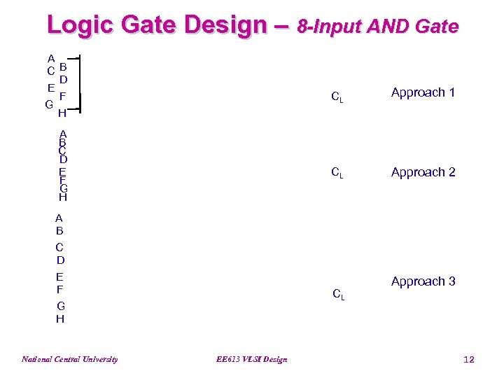 Logic Gate Design – 8 -Input AND Gate A CB D E F G H CL CL A B C D E F G H National Central University Approach 1 Approach 2 CL EE 613 VLSI Design Approach 3 12
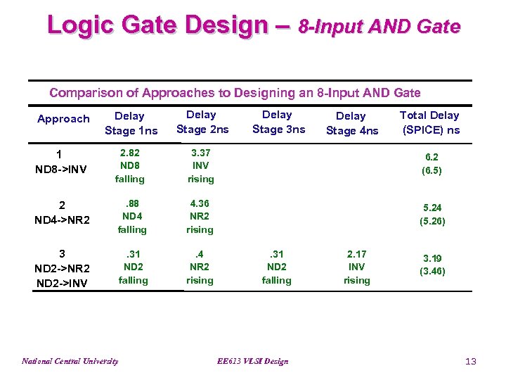 Logic Gate Design – 8 -Input AND Gate Comparison of Approaches to Designing an 8 -Input AND Gate Approach Delay Stage 1 ns Delay Stage 2 ns 1 ND 8 ->INV 2. 82 ND 8 falling 3. 37 INV rising 6. 2 (6. 5) 2 ND 4 ->NR 2 . 88 ND 4 falling 4. 36 NR 2 rising 5. 24 (5. 26) 3 ND 2 ->NR 2 ND 2 ->INV . 31 ND 2 falling . 4 NR 2 rising National Central University Delay Stage 3 ns . 31 ND 2 falling EE 613 VLSI Design Delay Stage 4 ns 2. 17 INV rising Total Delay (SPICE) ns 3. 19 (3. 46) 13
 Basic Physical Design • • Gates: Inverter, NAND, and NOR Complex Gates Standard Cells Gate Array Sea of Gates Layout Optimization Transmission Gates 2 -Input Multiplexer National Central University EE 613 VLSI Design 14
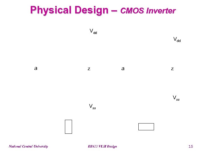 Physical Design – CMOS Inverter Vdd a z Vss National Central University EE 613 VLSI Design 15
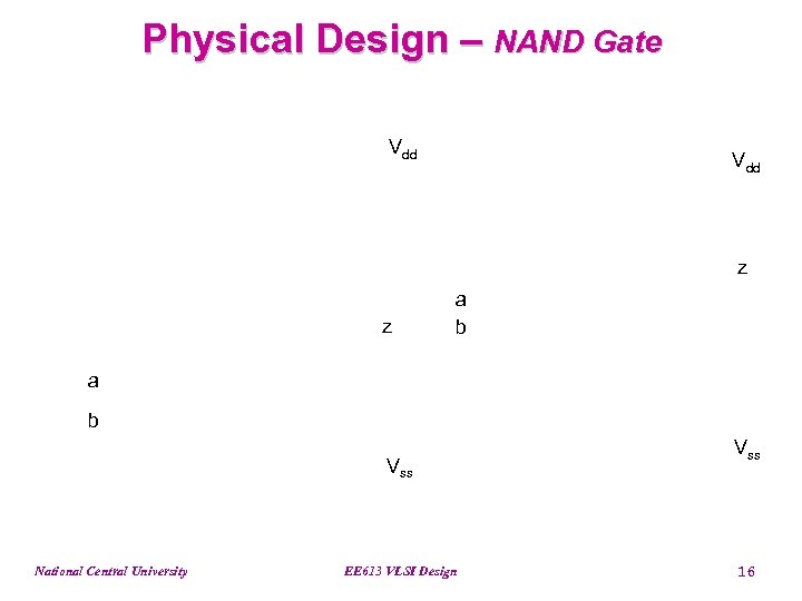 Physical Design – NAND Gate Vdd z z a b Vss National Central University EE 613 VLSI Design Vss 16
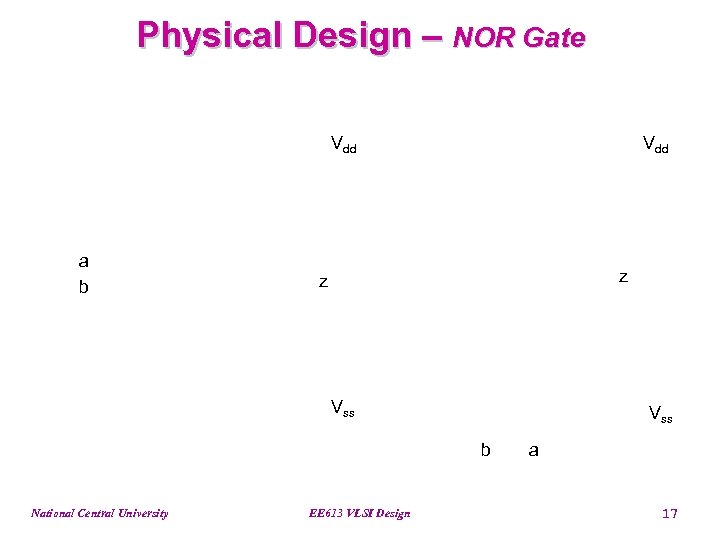 Physical Design – NOR Gate Vdd a b Vdd z z Vss b National Central University EE 613 VLSI Design a 17
 Physical Design – Complex Gates • All complex gates can be designed using a single row of N-transistors and a single row of Ptransistors, aligned at common gate connections • Design procedure - Draw two dual graphs to P transistor tree and N transistor tree - Find all Euler paths that cover the graph - Find a P and an N Euler path that have identical labeling - If not found, break the gate in the minimum numbers of places to achieve step 3 National Central University EE 613 VLSI Design 18
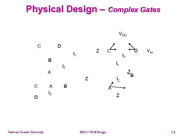 Physical Design – Complex Gates VDD C D Z I 1 C B I 3 A Z D National Central University A I 3 Vss I 1 I 2 C D B I 2 B A Z EE 613 VLSI Design 19
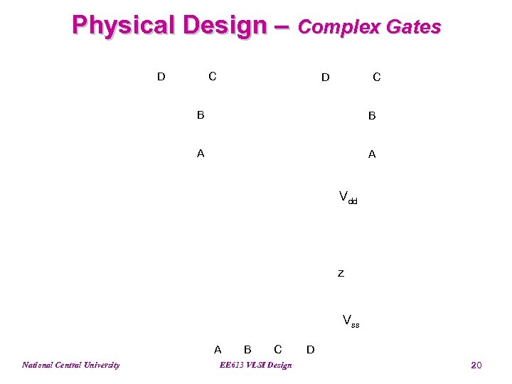 Physical Design – Complex Gates D C B B A A Vdd z Vss A National Central University B C EE 613 VLSI Design D 20
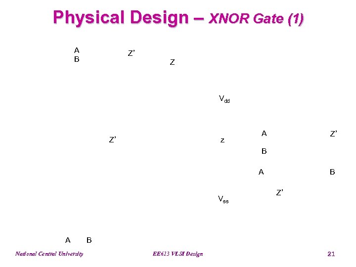 Physical Design – XNOR Gate (1) A B Z’ Z Vdd Z’ z A Z’ B A Vss A National Central University B Z’ B EE 613 VLSI Design 21
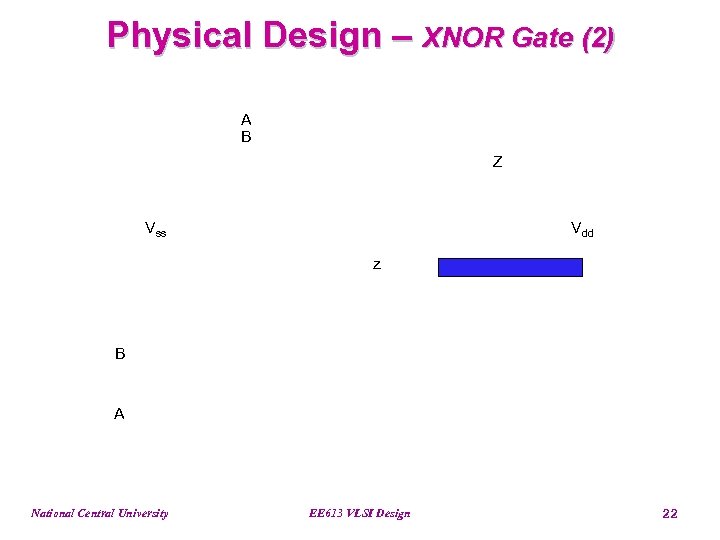 Physical Design – XNOR Gate (2) A B Z Vss Vdd z B A National Central University EE 613 VLSI Design 22
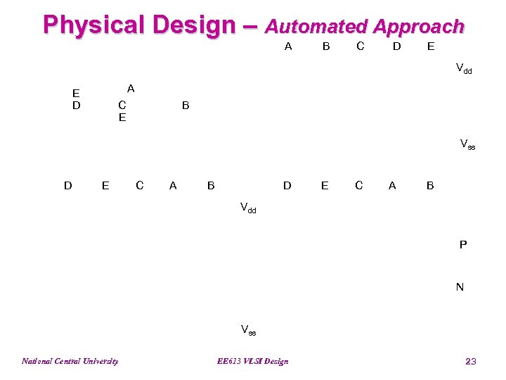 Physical Design – Automated Approach A B C D E Vdd A E D C E B Vss D E C A B Vdd P N Vss National Central University EE 613 VLSI Design 23
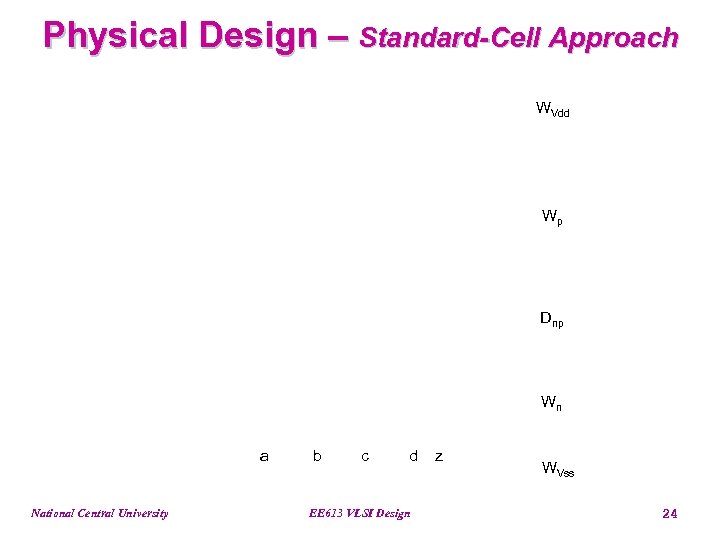 Physical Design – Standard-Cell Approach WVdd Wp Dnp Wn a National Central University b c d EE 613 VLSI Design z WVss 24
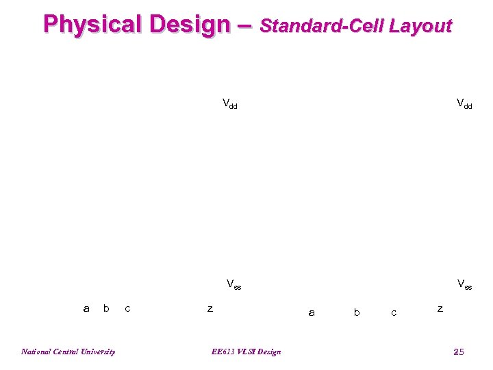 Physical Design – Standard-Cell Layout Vdd Vss a b National Central University c z EE 613 VLSI Design Vss a b c z 25
 Physical Design – Gate Array Layout (1) Vdd Vss National Central University EE 613 VLSI Design 26
 Physical Design – Gate Array Layout (2) Vdd Gate array cells Routing channels Vss National Central University EE 613 VLSI Design 27
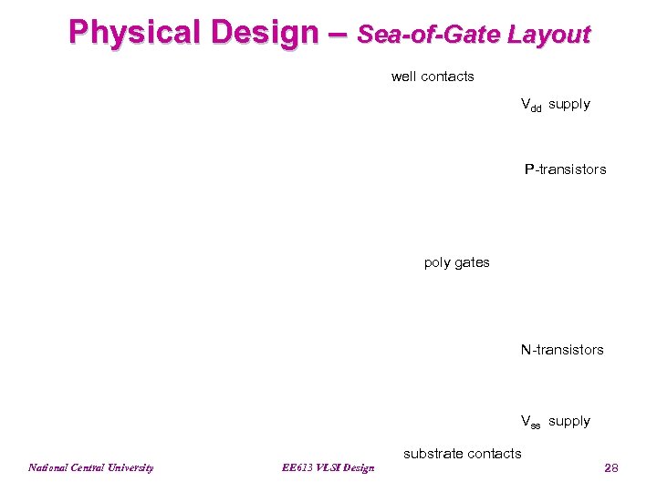 Physical Design – Sea-of-Gate Layout well contacts Vdd supply P-transistors poly gates N-transistors Vss supply substrate contacts National Central University EE 613 VLSI Design 28
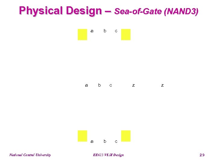 Physical Design – Sea-of-Gate (NAND 3) a a b a National Central University b c z c b z c EE 613 VLSI Design 29
 Physical Design – CMOS Layout Guidelines • Run VDD and VSS in metal at the top and bottom of the cell • • Run a vertical poly line for each gate input • Place n-gate segments close to VSS and p-gate segments close to VDD • Connection to complete the logic gate should be made in poly, metal, or, where appropriate, in diffusion Order the poly gate signals to allow the maximal connection between transistors via abutting source -drain connection. National Central University EE 613 VLSI Design 30
 Physical Design – Improvement in Density • Better use of routing layers – routes can occurs over cells • • • More “merged” source-drain connections More usage of “white” space in sparse gates Use of optimum device sizes – the use of smaller devices leads to smaller layouts National Central University EE 613 VLSI Design 31
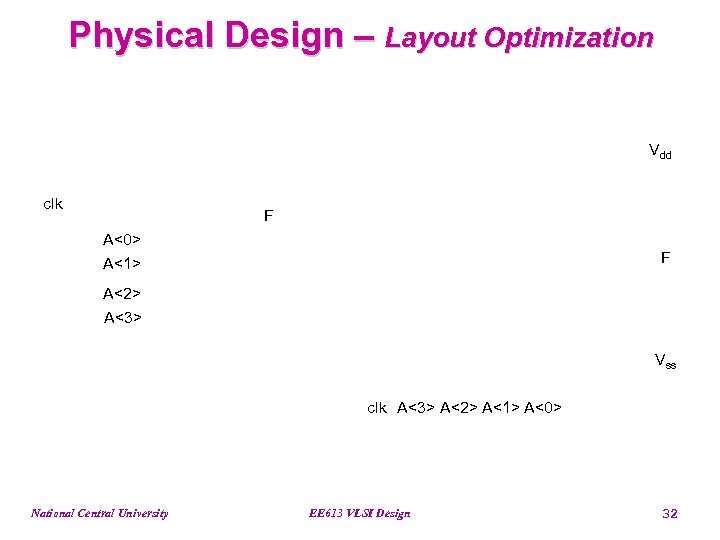 Physical Design – Layout Optimization Vdd clk F A<0> F A<1> A<2> A<3> Vss clk A<3> A<2> A<1> A<0> National Central University EE 613 VLSI Design 32
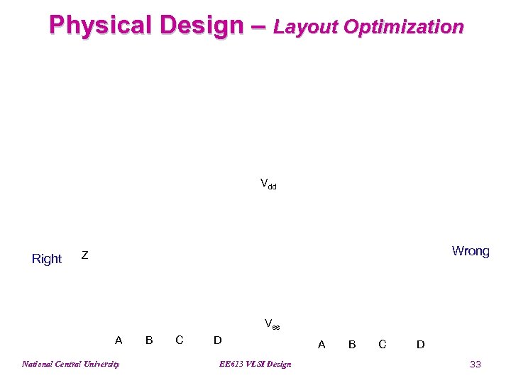 Physical Design – Layout Optimization Vdd Right Wrong Z Vss A National Central University B C D EE 613 VLSI Design A B C D 33
 Physical Design – Transmission Gate National Central University EE 613 VLSI Design 34
 Physical Design – Transmission Gate National Central University EE 613 VLSI Design 35
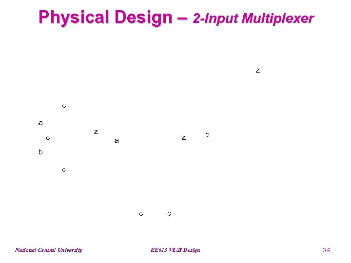 Physical Design – 2 -Input Multiplexer z c a z -c z a b b c c National Central University -c EE 613 VLSI Design 36
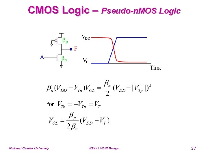 CMOS Logic – Pseudo-n. MOS Logic for National Central University EE 613 VLSI Design 37
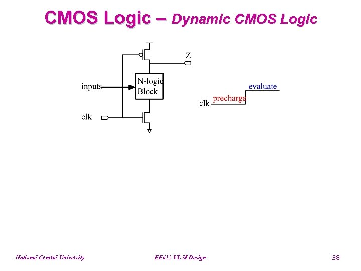 CMOS Logic – Dynamic CMOS Logic National Central University EE 613 VLSI Design 38
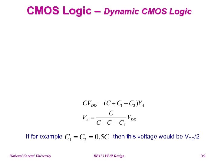 CMOS Logic – Dynamic CMOS Logic If for example National Central University then this voltage would be VDD/2 EE 613 VLSI Design 39
 CMOS Logic – Dynamic CMOS Logic National Central University EE 613 VLSI Design 40
 CMOS Logic – Clocked CMOS Logic National Central University EE 613 VLSI Design 41
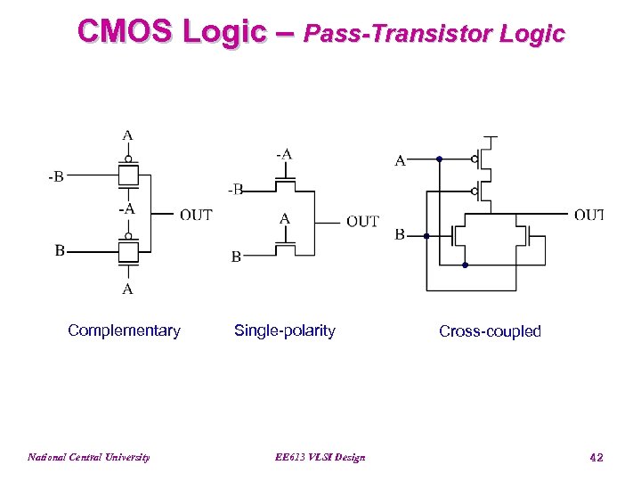 CMOS Logic – Pass-Transistor Logic Complementary National Central University Single-polarity EE 613 VLSI Design Cross-coupled 42
 CMOS Logic – CMOS Domino Logic Basic gate National Central University EE 613 VLSI Design 43
 CMOS Logic – CMOS Domino Logic Static version National Central University Latched version EE 613 VLSI Design 44
 CMOS Logic – CMOS Domino Logic National Central University EE 613 VLSI Design 45
 CMOS Logic – NP Domino Logic National Central University EE 613 VLSI Design 46
 CMOS Logic–Advantages of Dynamic Logic • • • Smaller area than fully static gates Smaller parasitic capacitance, hence higher speed Glitch free operation if designed carefully National Central University EE 613 VLSI Design 47
 CMOS Logic – CVSL Basic version National Central University A particular function EE 613 VLSI Design 48
 CMOS Logic – CVSL (abcd)=(0000) Clocked version National Central University A 4 -way XOR gate EE 613 VLSI Design 49
 Clocking Strategies – Clocked Systems Combinational Logic A simple finite state machine National Central University EE 613 VLSI Design 50
 Clocking Strategies – Clocked Systems A pipeline system National Central University EE 613 VLSI Design 51
 Clocking Strategies – Latches and Reg. Cycle time Tc National Central University EE 613 VLSI Design 52
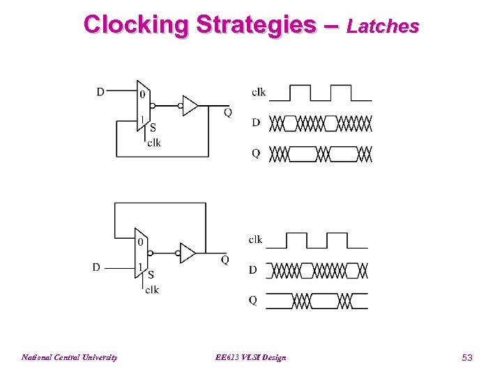 Clocking Strategies – Latches National Central University EE 613 VLSI Design 53
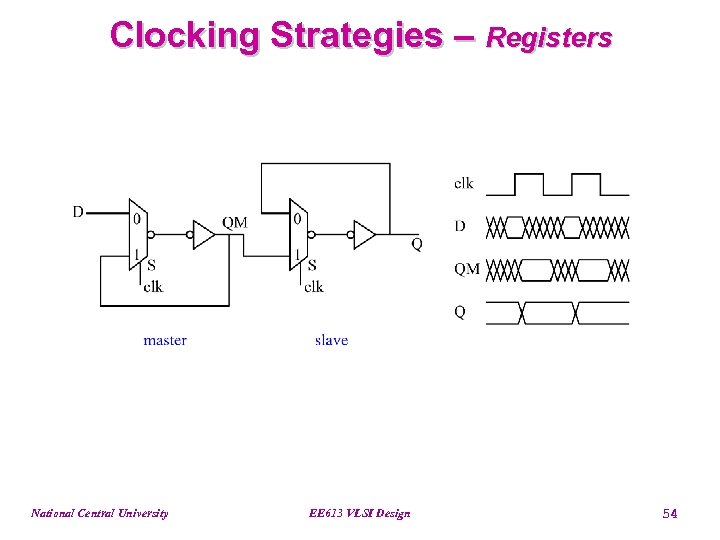 Clocking Strategies – Registers National Central University EE 613 VLSI Design 54
 Clocking Strategies – Registers National Central University EE 613 VLSI Design 55
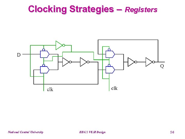 Clocking Strategies – Registers National Central University EE 613 VLSI Design 56
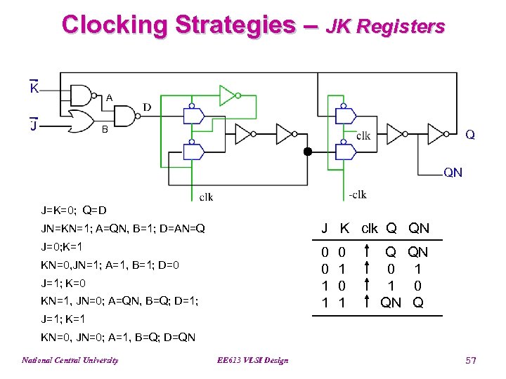 Clocking Strategies – JK Registers K A J B Q QN J=K=0; Q=D JN=KN=1; A=QN, B=1; D=AN=Q J K clk Q QN J=0; K=1 0 0 1 1 KN=0, JN=1; A=1, B=1; D=0 J=1; K=0 KN=1, JN=0; A=QN, B=Q; D=1; 0 1 QN QN 1 0 Q J=1; K=1 KN=0, JN=0; A=1, B=Q; D=QN National Central University EE 613 VLSI Design 57
 Clocking Strategies – System Timing National Central University EE 613 VLSI Design 58
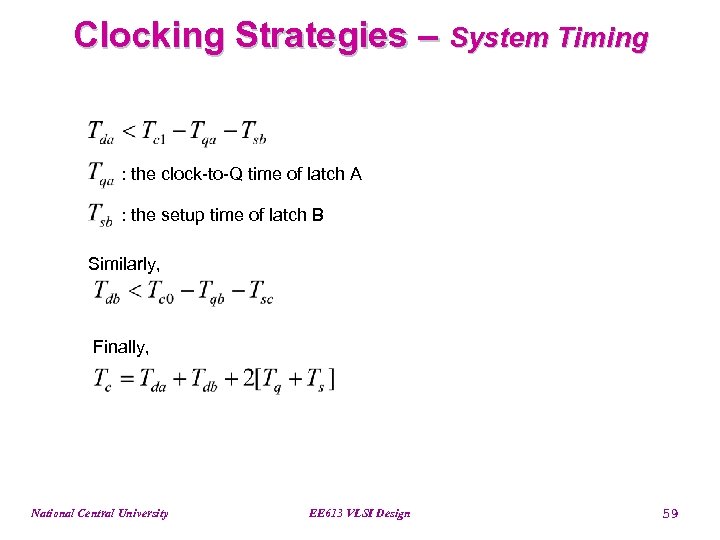 Clocking Strategies – System Timing : the clock-to-Q time of latch A : the setup time of latch B Similarly, Finally, National Central University EE 613 VLSI Design 59
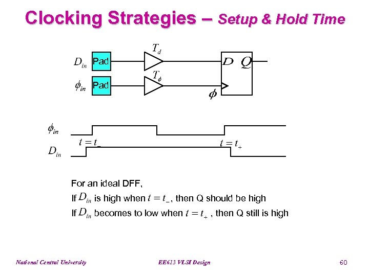 Clocking Strategies – Setup & Hold Time Pad For an ideal DFF, If is high when If becomes to low when National Central University , then Q should be high EE 613 VLSI Design , then Q still is high 60
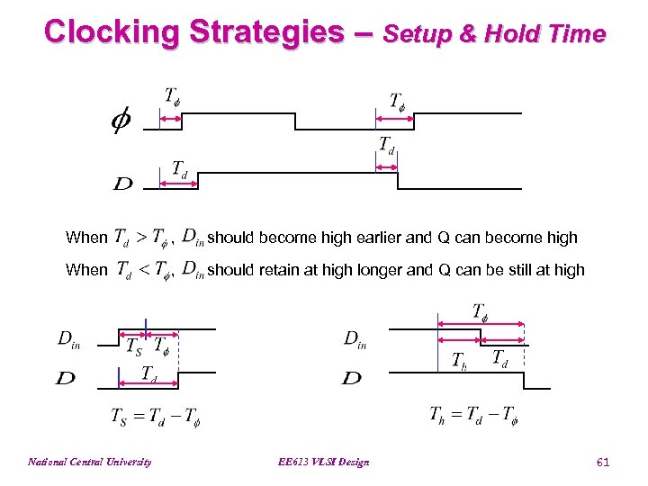 Clocking Strategies – Setup & Hold Time When , should become high earlier and Q can become high When , should retain at high longer and Q can be still at high National Central University EE 613 VLSI Design 61
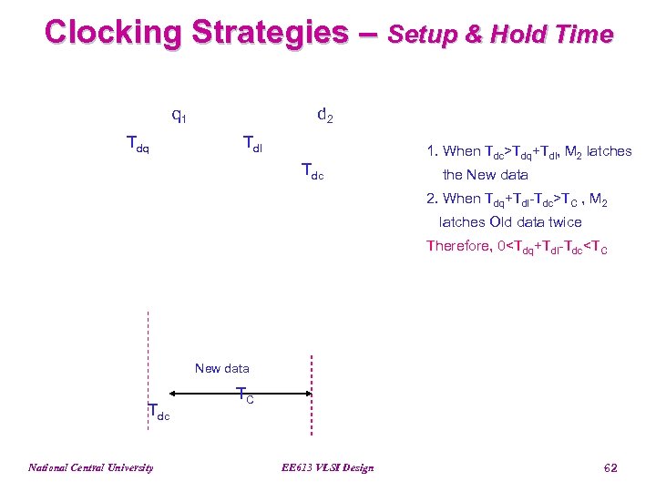 Clocking Strategies – Setup & Hold Time q 1 Tdq d 2 Tdl Tdc 1. When Tdc>Tdq+Tdl, M 2 latches the New data 2. When Tdq+Tdl-Tdc>TC , M 2 latches Old data twice Therefore, 0
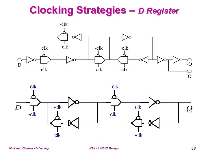 Clocking Strategies – D Register clk -clk clk National Central University -clk EE 613 VLSI Design 63
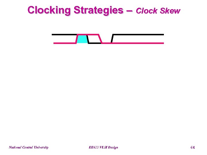 Clocking Strategies – Clock Skew National Central University EE 613 VLSI Design 64
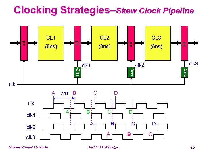 Clocking Strategies–Skew Clock Pipeline CL 2 (9 ns) (5 ns) clk 3 -2 ns 0 ns -2 ns clk 2 clk 1 FF (5 ns) CL 3 FF FF FF CL 1 clk A 7 ns B C D clk 1 clk 2 clk 3 National Central University A B C A D B A EE 613 VLSI Design C B D C 65
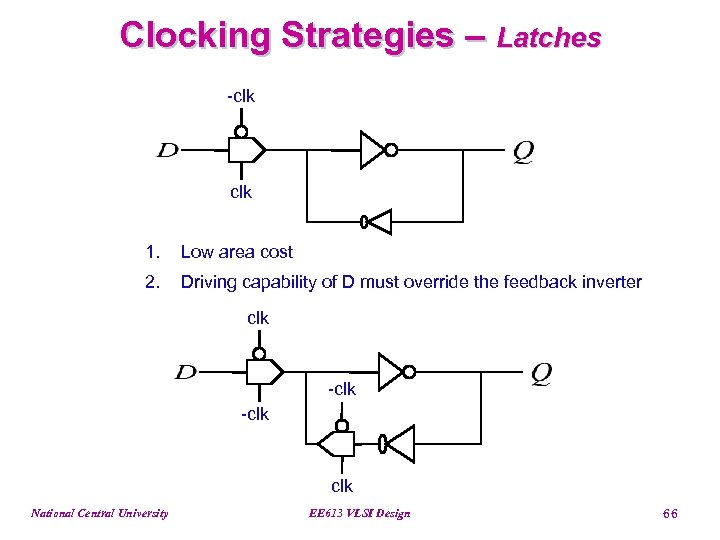 Clocking Strategies – Latches -clk 1. Low area cost 2. Driving capability of D must override the feedback inverter clk -clk National Central University EE 613 VLSI Design 66
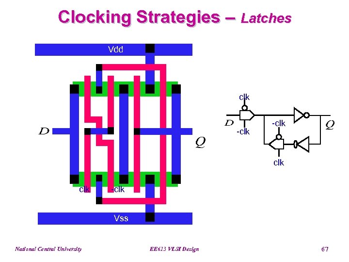 Clocking Strategies – Latches Vdd clk -clk Vss National Central University EE 613 VLSI Design 67
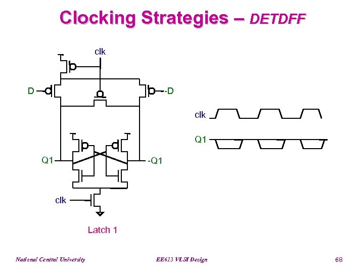 Clocking Strategies – DETDFF clk D -D clk Q 1 -Q 1 clk Latch 1 National Central University EE 613 VLSI Design 68
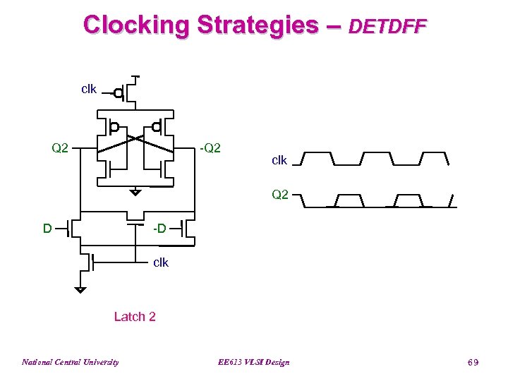 Clocking Strategies – DETDFF clk Q 2 -Q 2 clk Q 2 D -D clk Latch 2 National Central University EE 613 VLSI Design 69
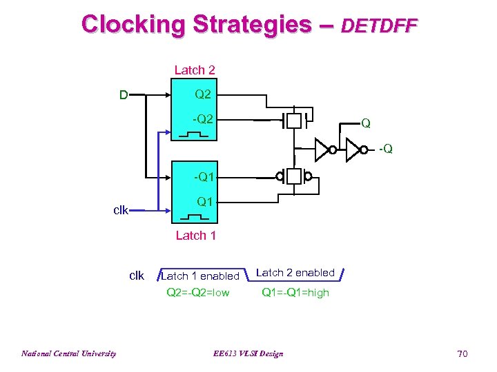 Clocking Strategies – DETDFF Latch 2 Q 2 D -Q 2 Q -Q -Q 1 clk Latch 1 clk National Central University Latch 1 enabled Q 2=-Q 2=low Latch 2 enabled Q 1=-Q 1=high EE 613 VLSI Design 70
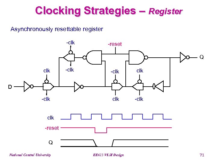 Clocking Strategies – Register Asynchronously resettable register -clk -reset Q clk -clk D -clk -reset Q National Central University EE 613 VLSI Design 71
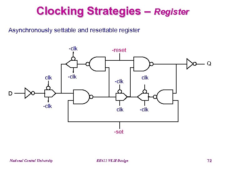 Clocking Strategies – Register Asynchronously settable and resettable register -clk -reset Q clk -clk D -clk -set National Central University EE 613 VLSI Design 72
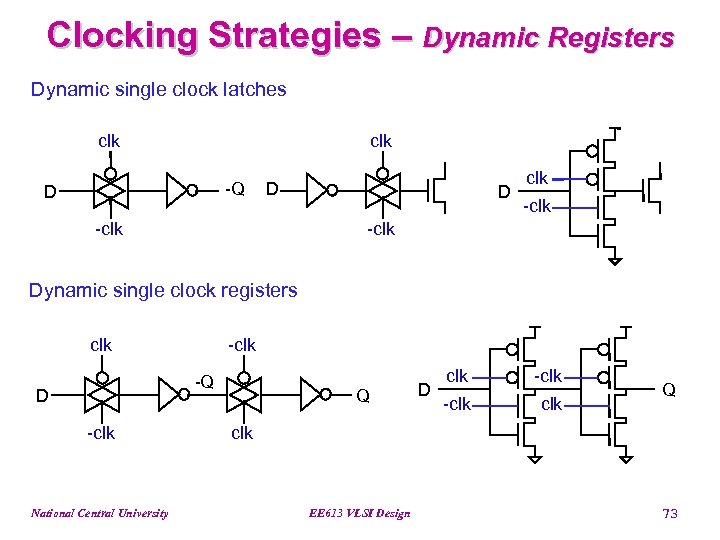 Clocking Strategies – Dynamic Registers Dynamic single clock latches clk -Q D D -clk D clk -clk Dynamic single clock registers clk -Q D -clk National Central University Q D clk -clk Q clk EE 613 VLSI Design 73
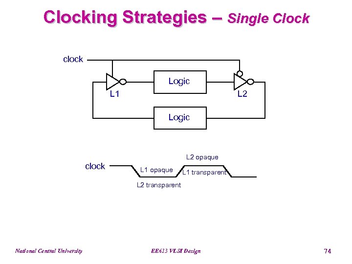 Clocking Strategies – Single Clock clock Logic L 1 L 2 Logic L 2 opaque clock L 1 opaque L 1 transparent L 2 transparent National Central University EE 613 VLSI Design 74
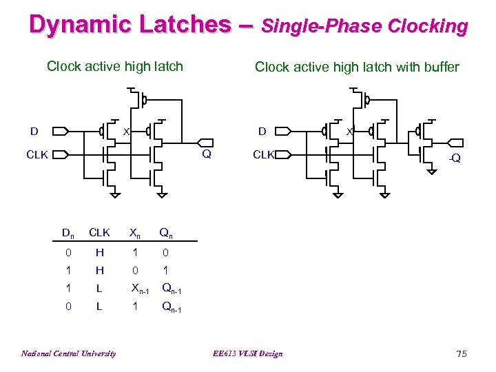 Dynamic Latches – Single-Phase Clocking Clock active high latch D Clock active high latch with buffer D X Q CLK Dn CLK Xn H 1 0 1 H 0 1 1 L Xn-1 Qn-1 0 L 1 -Q Qn 0 CLK X Qn-1 National Central University EE 613 VLSI Design 75
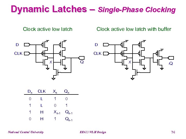 Dynamic Latches – Single-Phase Clocking Clock active low latch with buffer D D CLK Q X Dn CLK Xn L 1 0 1 L 0 1 1 H Xn-1 Qn-1 0 H 1 -Q Qn 0 X Qn-1 National Central University EE 613 VLSI Design 76
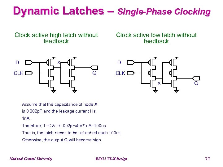 Dynamic Latches – Single-Phase Clocking Clock active high latch without feedback Clock active low latch without feedback D D X CLK Q CLK X Q Assume that the capacitance of node X is 0. 002 p. F and the leakage current I is 1 n. A. Therefore, T=CV/I=0. 002 p. Fx 5 V/1 n. A=100 us. That is, the latch needs to be refreshed each 100 us. Otherwise, the output Q will become high. National Central University EE 613 VLSI Design 77
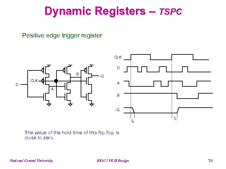 Dynamic Registers – TSPC Positive edge trigger register CLK D B D CLK -Q A A B -Q tf tr The value of the hold time of this flip flop is close to zero. National Central University EE 613 VLSI Design 78
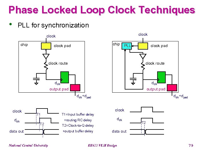 Phase Locked Loop Clock Techniques • PLL for synchronization clock chip clock pad PLL clock pad clock route dclk output pad dclk+dpad clock T 1=Input buffer delay +routing RC delay T 2 data out National Central University dclk T 2=Clock-to-Q delay +output buffer delay T 2 data out EE 613 VLSI Design 79
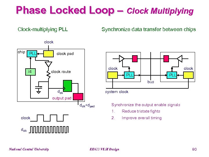 Phase Locked Loop – Clock Multiplying Clock-multiplying PLL Synchronize data transfer between chips clock chip PLL /4 clock pad clock route clock PLL bus dclk system clock output pad dclk+dpad Synchronize the output enable signals 1. clock Reduce tristate fights 2. Improve overall timing dclk National Central University EE 613 VLSI Design 80
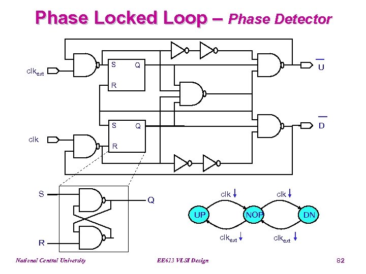
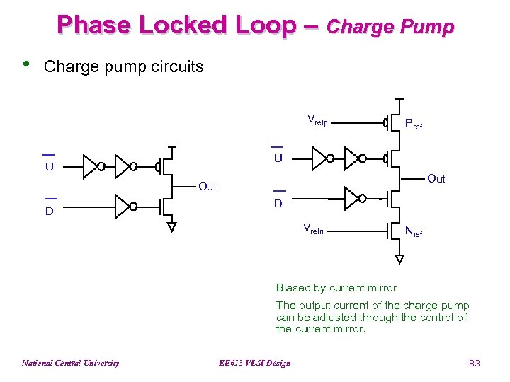
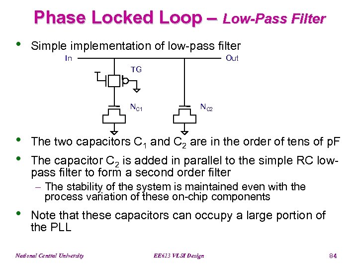
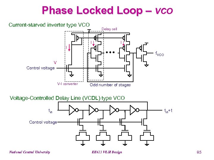
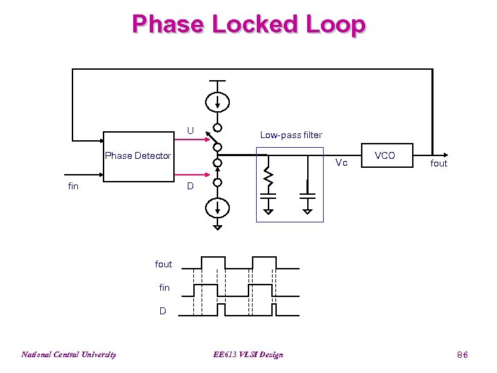
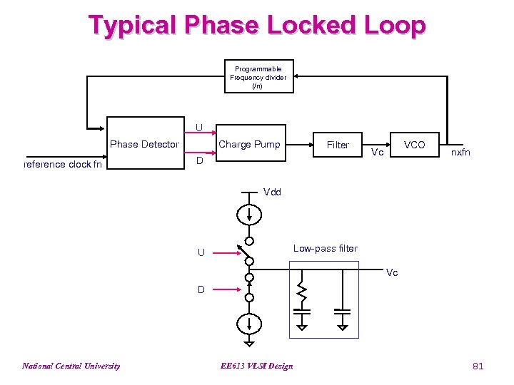 Typical Phase Locked Loop Programmable Frequency divider (/n) U Phase Detector reference clock fn Charge Pump Filter D VCO Vc nxfn Vdd Low-pass filter U Vc D National Central University EE 613 VLSI Design 81
 Phase Locked Loop – Phase Detector clkext S Q U Q D R S clk Q UP National Central University NOP clkext R EE 613 VLSI Design clk DN clkext 82
 Phase Locked Loop – Charge Pump • Charge pump circuits Vrefp Pref U U Out D D Vrefn Nref Biased by current mirror The output current of the charge pump can be adjusted through the control of the current mirror. National Central University EE 613 VLSI Design 83
 Phase Locked Loop – Low-Pass Filter • Simplementation of low-pass filter In Out TG NC 1 • • NC 2 The two capacitors C 1 and C 2 are in the order of tens of p. F The capacitor C 2 is added in parallel to the simple RC lowpass filter to form a second order filter - The stability of the system is maintained even with the process variation of these on-chip components • Note that these capacitors can occupy a large portion of the PLL National Central University EE 613 VLSI Design 84
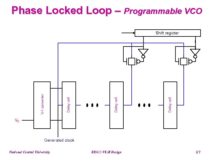
 Phase Locked Loop – VCO Current-starved inverter type VCO Delay cell I I I f. VCO V Control voltage V-I converter Odd number of stages Voltage-Controlled Delay Line (VCDL) type VCO tin+t Control voltage National Central University EE 613 VLSI Design 85
 Phase Locked Loop U Low-pass filter Phase Detector fin Vc VCO fout D fout fin D National Central University EE 613 VLSI Design 86
 Phase Locked Loop – Programmable VCO Delay cell V-I converter Shift register VC Generated clock National Central University EE 613 VLSI Design 87
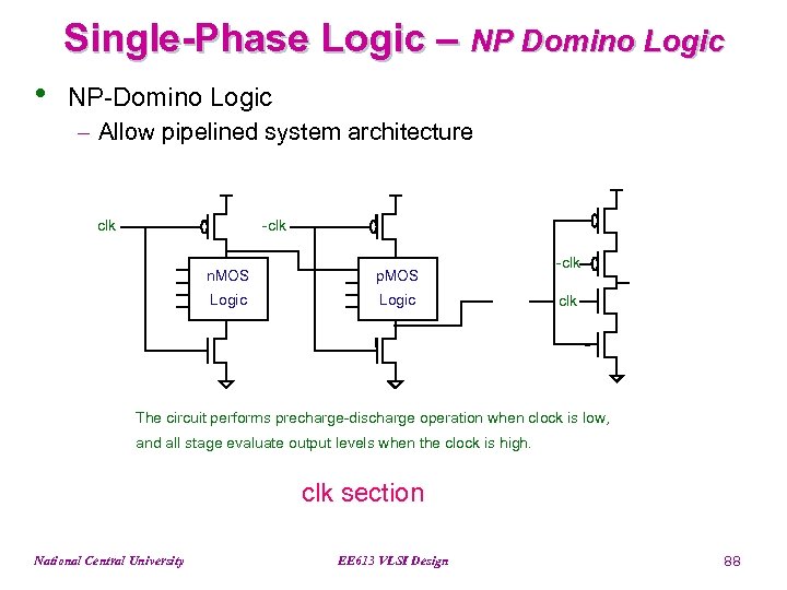 Single-Phase Logic – NP Domino Logic • NP-Domino Logic - Allow pipelined system architecture clk -clk n. MOS p. MOS Logic -clk The circuit performs precharge-discharge operation when clock is low, and all stage evaluate output levels when the clock is high. clk section National Central University EE 613 VLSI Design 88
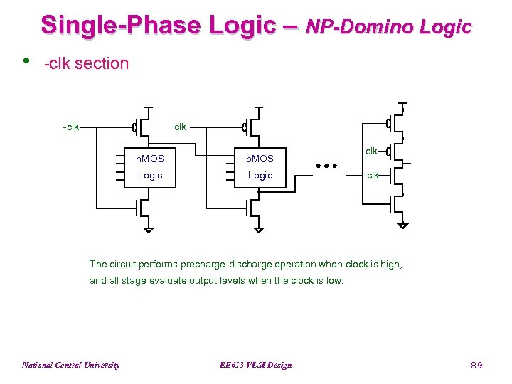 Single-Phase Logic – NP-Domino Logic • -clk section -clk n. MOS p. MOS Logic clk -clk The circuit performs precharge-discharge operation when clock is high, and all stage evaluate output levels when the clock is low. National Central University EE 613 VLSI Design 89
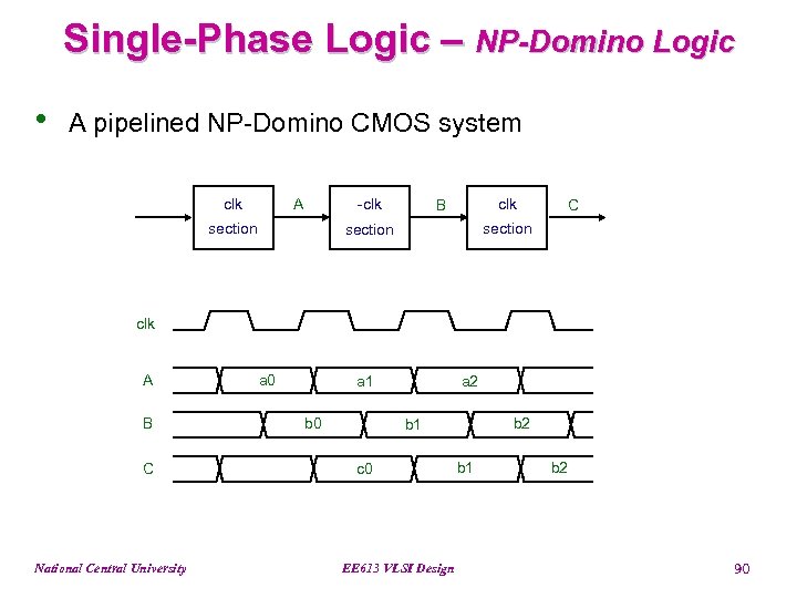 Single-Phase Logic – NP-Domino Logic • A pipelined NP-Domino CMOS system clk A -clk section clk B C section clk A B C National Central University a 0 a 2 a 1 b 0 b 2 b 1 c 0 EE 613 VLSI Design b 1 b 2 90
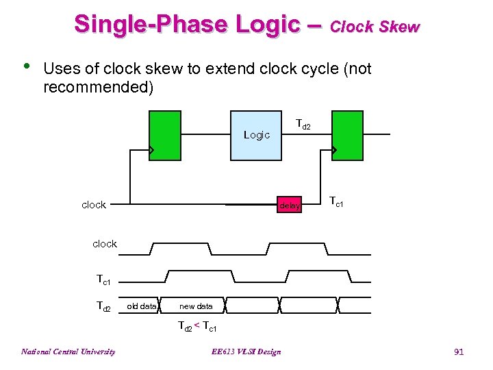 Single-Phase Logic – Clock Skew • Uses of clock skew to extend clock cycle (not recommended) Td 2 Logic clock delay Tc 1 clock Tc 1 Td 2 old data new data Td 2 < Tc 1 National Central University EE 613 VLSI Design 91
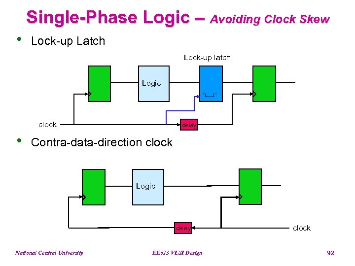 Single-Phase Logic – Avoiding Clock Skew • Lock-up Latch Lock-up latch Logic clock • delay Contra-data-direction clock Logic delay National Central University EE 613 VLSI Design clock 92
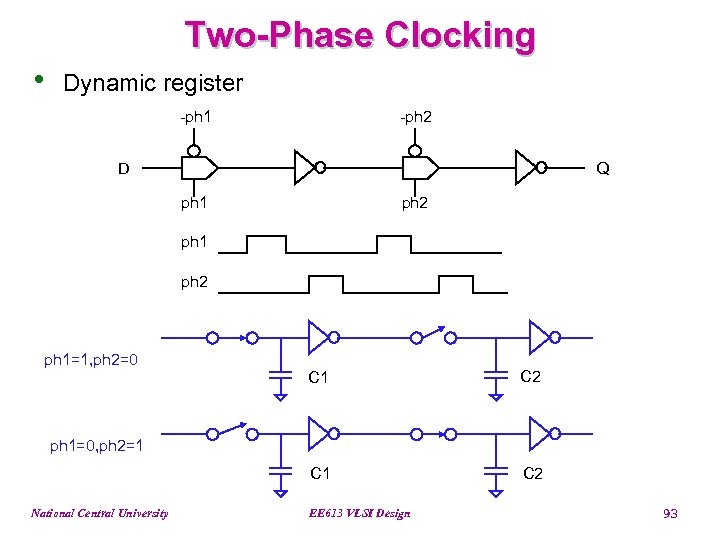 Two-Phase Clocking • Dynamic register -ph 1 -ph 2 D Q ph 1 ph 2 ph 1=1, ph 2=0 C 1 C 2 ph 1=0, ph 2=1 National Central University EE 613 VLSI Design 93
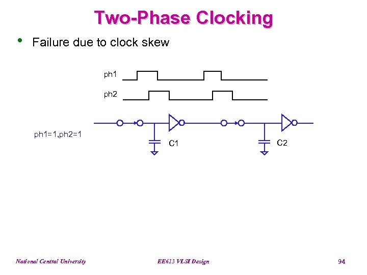 Two-Phase Clocking • Failure due to clock skew ph 1 ph 2 ph 1=1, ph 2=1 C 1 National Central University EE 613 VLSI Design C 2 94
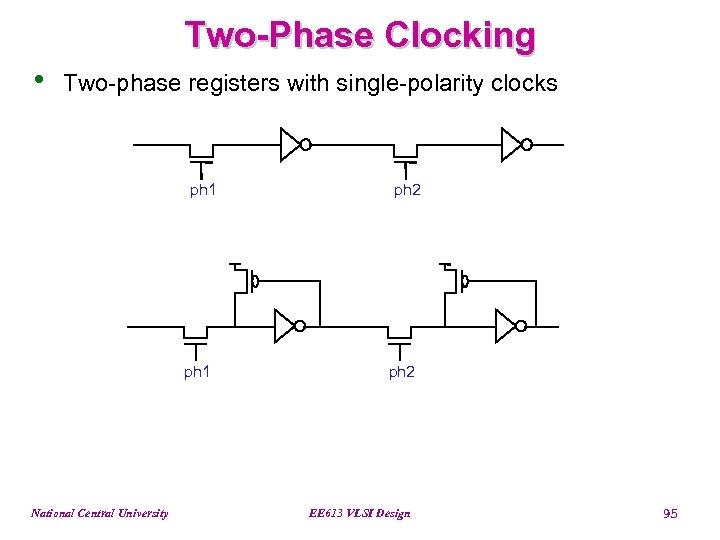 Two-Phase Clocking • Two-phase registers with single-polarity clocks ph 1 National Central University ph 2 EE 613 VLSI Design 95
 Clock Distribution • In a large CMOS chip, clock distribution is a serious problem - • Vdd=5 V Creg=2000 p. F (20 K register bits @ 0. 1 p. F) Tclk=10 ns Trise/fall=1 ns Ipeak=Cdv/dt=(2000 px 5)/1 n=10 A Pd=CVdd 2 f=2000 px 25 x 100=5 W Methods for reducing the values of Ipeak and Pd - Reduce C - Interleaving the rise/fall time National Central University EE 613 VLSI Design 96
 Clock Distribution • Clocking is a floorplanning problem because clock delay varies with position on the chip • Ways to improve clock distribution - Physical design * Make clock delays more even * At least more predictable - Circuit design * Minimizing delays using several stages of drivers • Two most common types of physical clocking networks - H tree - Balanced tree National Central University EE 613 VLSI Design 97
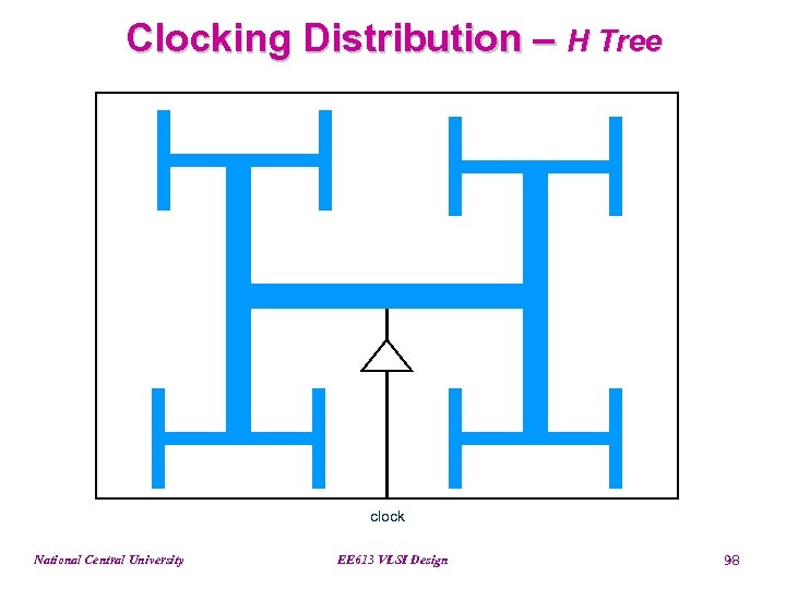 Clocking Distribution – H Tree clock National Central University EE 613 VLSI Design 98
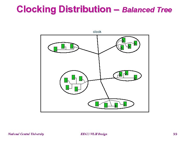 Clocking Distribution – Balanced Tree clock National Central University EE 613 VLSI Design 99
 Clocking Distribution – Reducing Power • Techniques used to reduce the high dynamic power dissipation - Use a low capacitance clock routing line such as metal 3. This layer of metal can be, for example, dedicated to clock distribution only - Using low-swing drivers at the top level of the tree or in intermediate levels National Central University EE 613 VLSI Design 100
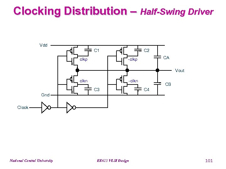 Clocking Distribution – Half-Swing Driver Vdd C 1 clkp C 2 CA -clkp Vout clkn -clkn C 3 CB C 4 Gnd Clock National Central University EE 613 VLSI Design 101
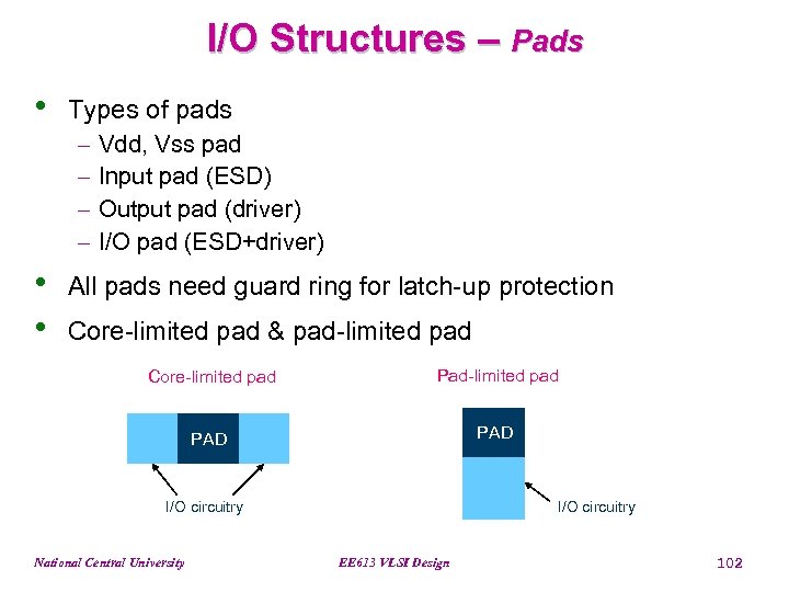 I/O Structures – Pads • Types of pads - • • Vdd, Vss pad Input pad (ESD) Output pad (driver) I/O pad (ESD+driver) All pads need guard ring for latch-up protection Core-limited pad & pad-limited pad Core-limited pad Pad-limited pad PAD I/O circuitry National Central University EE 613 VLSI Design 102
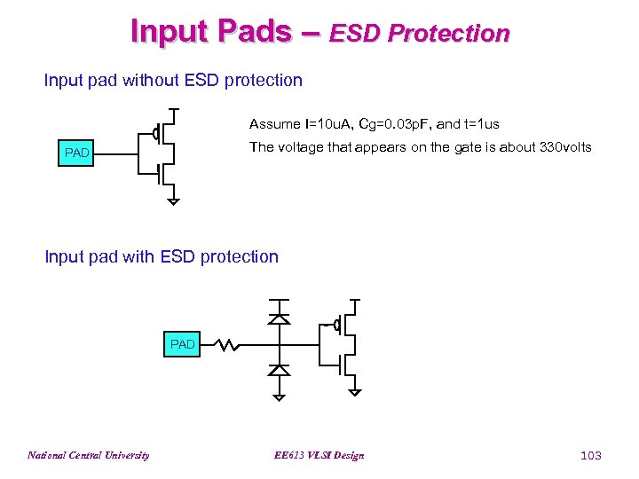 Input Pads – ESD Protection Input pad without ESD protection Assume I=10 u. A, Cg=0. 03 p. F, and t=1 us The voltage that appears on the gate is about 330 volts PAD Input pad with ESD protection PAD National Central University EE 613 VLSI Design 103
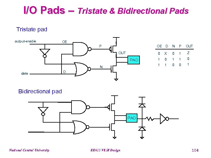 I/O Pads – Tristate & Bidirectional Pads Tristate pad output-enable OE P OE OUT N P OUT 0 N X 0 1 Z 1 0 1 PAD data D 1 0 0 1 D Bidirectional pad PAD National Central University EE 613 VLSI Design 104
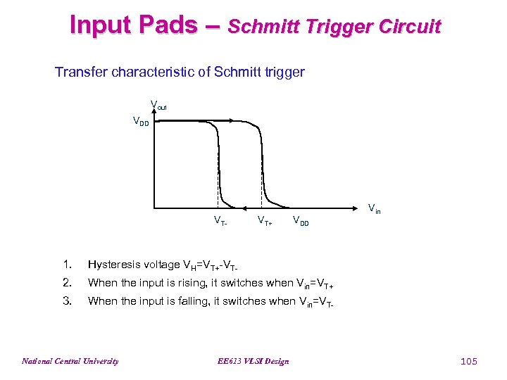 Input Pads – Schmitt Trigger Circuit Transfer characteristic of Schmitt trigger Vout VDD VT- VT+ VDD 1. Hysteresis voltage VH=VT+-VT- 2. When the input is rising, it switches when Vin=VT+ 3. Vin When the input is falling, it switches when Vin=VT- National Central University EE 613 VLSI Design 105
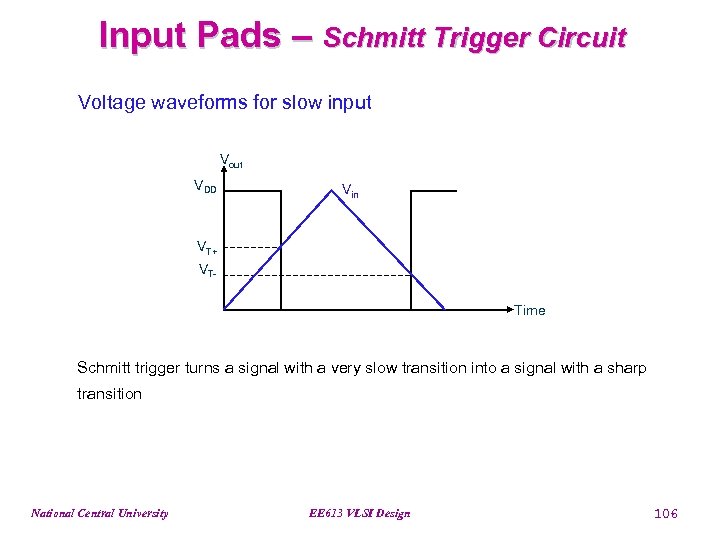 Input Pads – Schmitt Trigger Circuit Voltage waveforms for slow input Vout VDD Vin VT+ VTTime Schmitt trigger turns a signal with a very slow transition into a signal with a sharp transition National Central University EE 613 VLSI Design 106
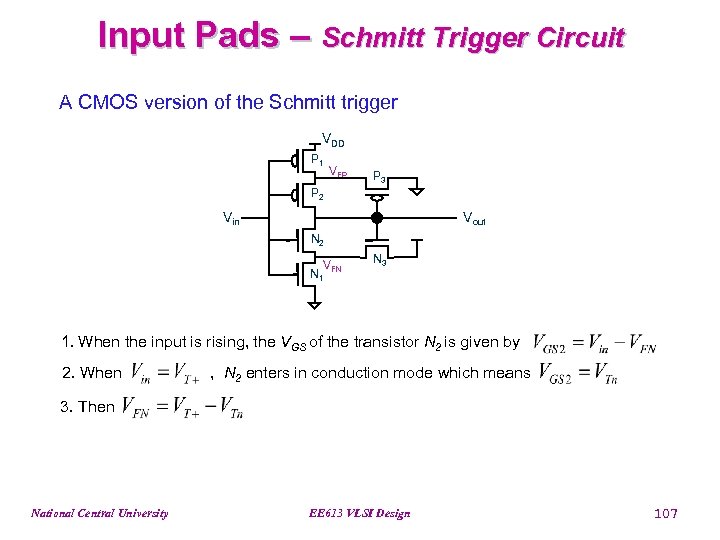 Input Pads – Schmitt Trigger Circuit A CMOS version of the Schmitt trigger VDD P 1 VFP P 3 P 2 Vin Vout N 2 VFN N 1 N 3 1. When the input is rising, the VGS of the transistor N 2 is given by 2. When , N 2 enters in conduction mode which means 3. Then National Central University EE 613 VLSI Design 107


