0f8d0cf4b629a7e874e55f6018ec985d.ppt
- Количество слайдов: 36
 Vertical integration. . . VERTEX_08 28/07 -01/08/2008 Vertical Integration of Integrated Circuits and Pixel Detectors Grzegorz DEPTUCH Fermi National Accelerator Laboratory, Batavia, IL, USA on behalf of the FERMILAB ASIC design group: R. Yarema ldr. , G. Deptuch, J. Hoff, A. Shenai, M. Trimpl, T. Zimmerman and: M. Demarteau, R. Lipton, M. Turqueti, R. Rivera and others 8 focus of this presentation is 1) introduction to 3 D integration technology 2) design of first 3 D integrated device for HEP (including results) 3) discussion email: deptuch@ieee. org 1
 Vertical integration. . . VERTEX_08 28/07 -01/08/2008 Is 3 D (vertical integration) new? 8 For decades, semiconductor manufacturers have been shrinking transistors sizes in ICs to achieve the yearly increases in speed and performance described by Moore’s Law (chip performance will double every ~18 months) - Moore’s Law exists only because the RC delay has been negligible in comparison with signal propagation delay. It turns ou that for submicron technology, RC delay becomes a dominant factor! (the change to Cu interconnects, low-k ILDs and CMP is not giving answer to the questions: how to reduce RCs? ) 2
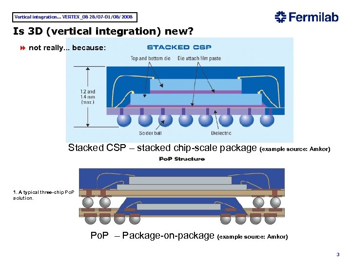 Vertical integration. . . VERTEX_08 28/07 -01/08/2008 Is 3 D (vertical integration) new? 8 not really. . . because: Stacked CSP – stacked chip-scale package (example source: Amkor) 1. A typical three-chip Po. P solution. Po. P – Package-on-package (example source: Amkor) 3
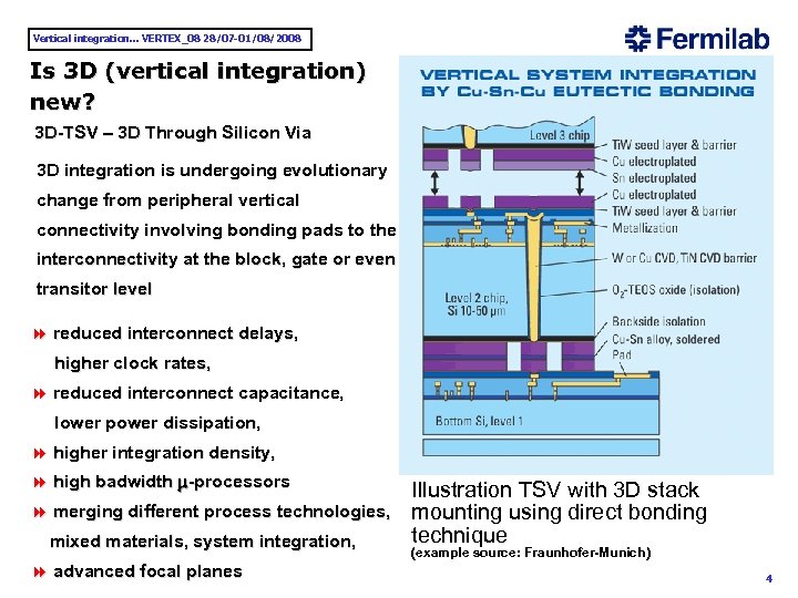 Vertical integration. . . VERTEX_08 28/07 -01/08/2008 Is 3 D (vertical integration) new? 3 D-TSV – 3 D Through Silicon Via 3 D integration is undergoing evolutionary change from peripheral vertical connectivity involving bonding pads to the interconnectivity at the block, gate or even transitor level 8 reduced interconnect delays, higher clock rates, 8 reduced interconnect capacitance, lower power dissipation, 8 higher integration density, 8 high badwidth m-processors 8 merging different process technologies, mixed materials, system integration, 8 advanced focal planes Illustration TSV with 3 D stack mounting using direct bonding technique (example source: Fraunhofer-Munich) 4
 Vertical integration. . . VERTEX_08 28/07 -01/08/2008 Challenges for 3 D-TSV technology: 3 D-TSV will be adopted , but to what extend and how quickly depends on: 8 Commercial availability of EDA tools and design methodologies, 8 Thermal concerns caused by the increased power densities, 8 Vendor adoption of TSV technology - Via first - foundries - Via last - 3 rd party vendors 8 Testability methods, known good die are availability 5
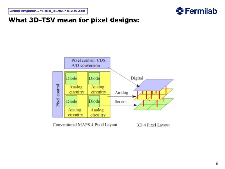 Vertical integration. . . VERTEX_08 28/07 -01/08/2008 What 3 D-TSV mean for pixel designs: 6
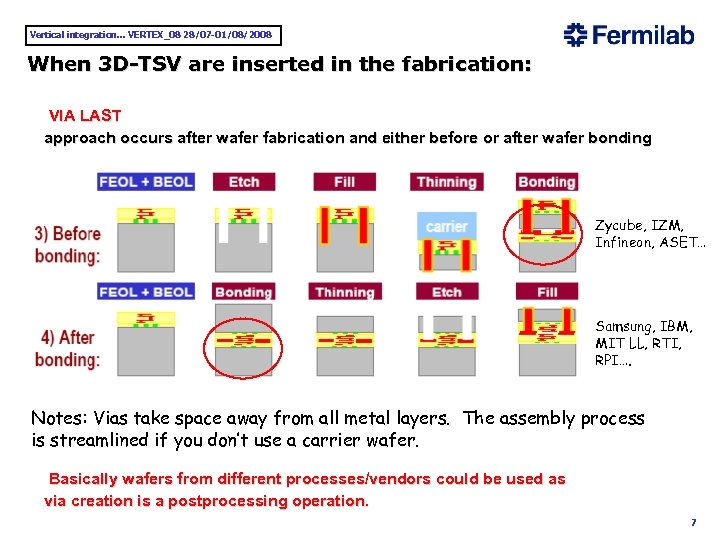 Vertical integration. . . VERTEX_08 28/07 -01/08/2008 When 3 D-TSV are inserted in the fabrication: VIA LAST approach occurs after wafer fabrication and either before or after wafer bonding Zycube, IZM, Infineon, ASET… Samsung, IBM, MIT LL, RTI, RPI…. Notes: Vias take space away from all metal layers. The assembly process is streamlined if you don’t use a carrier wafer. Basically wafers from different processes/vendors could be used as via creation is a postprocessing operation. 7
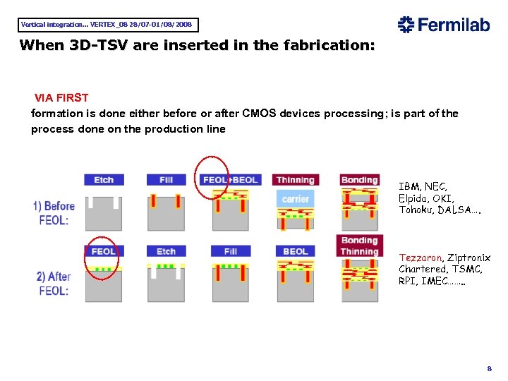 Vertical integration. . . VERTEX_08 28/07 -01/08/2008 When 3 D-TSV are inserted in the fabrication: VIA FIRST formation is done either before or after CMOS devices processing ; is part of the process done on the production line IBM, NEC, Elpida, OKI, Tohoku, DALSA…. Tezzaron, Ziptronix Chartered, TSMC, RPI, IMEC……. . 8
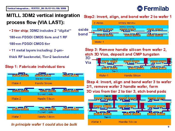 Vertical integration. . . VERTEX_08 28/07 -01/08/2008 MITLL 3 DM 2 vertical integration process flow (VIA LAST): • 3 tier chip; 3 DM 2 includes 2 “digital” 180 -nm FDSOI CMOS tiers and 1 RF Step 2: Invert, align, and bond wafer 2 to wafer 1 oxide bond 180 -nm FDSOI CMOS tier • 11 metal layers including: 2 -μmthick RF backmetal, Tier-2 backmetal Step 1: Fabricate individual tiers Step 3: Remove handle silicon from wafer 2, etch 3 D Vias, deposit and CMP tungsten 3 D Via Step 4: Invert, align and bond wafer 3 to wafer 2/1, remove wafer 3 handle wafer, form 3 D vias from tier 2 to tier 3, etch bond pads In principle wafer 1 could also be bulk 9
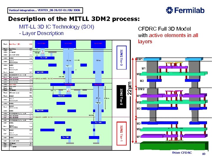 Vertical integration. . . VERTEX_08 28/07 -01/08/2008 Description of the MITLL 3 DM 2 process: MIT-LL 3 D IC Technology (SOI) - Layer Description CFDRC Full 3 D Model with active elements in all layers BM 1 22 mm M 2 M 3 BM 2 M 1 M 2 M 3 M 2 M 1 from CFDRC 10
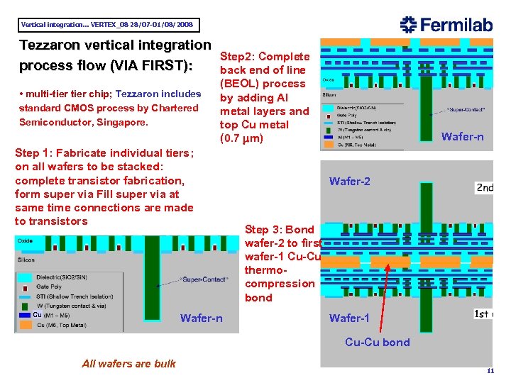 Vertical integration. . . VERTEX_08 28/07 -01/08/2008 Tezzaron vertical integration process flow (VIA FIRST): • multi-tier chip; Tezzaron includes standard CMOS process by Chartered Semiconductor, Singapore. Step 2: Complete back end of line (BEOL) process by adding Al metal layers and top Cu metal (0. 7 mm) Step 1: Fabricate individual tiers; on all wafers to be stacked: complete transistor fabrication, form super via Fill super via at same time connections are made to transistors Cu Wafer-n Wafer-2 Step 3: Bond wafer-2 to first wafer-1 Cu-Cu thermocompression bond Wafer-1 Cu-Cu bond All wafers are bulk 11
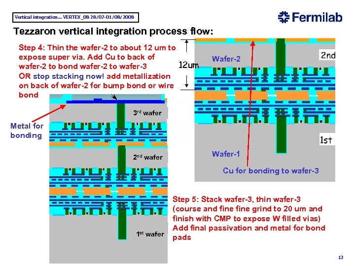 Vertical integration. . . VERTEX_08 28/07 -01/08/2008 Tezzaron vertical integration process flow: Step 4: Thin the wafer-2 to about 12 um to expose super via. Add Cu to back of 12 um wafer-2 to bond wafer-2 to wafer-3 OR stop stacking now! add metallization on back of wafer-2 for bump bond or wire bond Wafer-2 3 rd wafer Metal for bonding 2 nd wafer Wafer-1 Cu for bonding to wafer-3 1 st wafer Step 5: Stack wafer-3, thin wafer-3 (course and fine grind to 20 um and finish with CMP to expose W filled vias) Add final passivation and metal for bond pads 12
 Vertical integration. . . VERTEX_08 28/07 -01/08/2008 3 D-Integration activities at FERMILAB 8 FERMILAB work on vertical integration technologies started in 2006. 8 Efforts include: - design of 3 D integrated circuit exploitng 3 D TSV, - wafer thinning and investigations of interconnectivity RO/detector (low profile, low material budget, high density, interconnects), - design of monolithic detector/readout systems in So. I on HR handle wafer. 8 3 D - integration related work: - design of 3 D integrated readout circuit with architecure for ILC (VIP vertically integrated pixel) in 0. 18 mm MITLL 3 DM 2 process (Oct. 2006) – tests performed, - new VIP 2, 0. 15 mm MITLL 3 DM 3 process (tape out Sept. 30 2008) - new 3 D design exploring commercial 3 D integration technology by Tezzaron built on Chartered Sem. 0. 13 mm CMOS process – FERMILAB hosts MPW (reticle shared between interested users) - wafer thinning and laser annealing for low material budget detectors – underway with different vendors (IZM, RTI, Ziptronix, MITLL), - investigation of low mass, high density bonding. 13
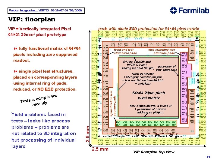 Vertical integration. . . VERTEX_08 28/07 -01/08/2008 VIP: floorplan pads with diode ESD protection for 64× 64 pixel matrix VIP = Vertically Integrated Pixel 64× 64 20 mm 2 pixel prototype 8 fully functional matrix of 64× 64 pixels including zero suppresed readout, front-end test structures pads drivers data. Clk and inj. Clk (30 mm) + analog readout (60 mm) 8 single pixel test structures, placed on corresponding layers using internal ring of pads, reduced, or NO ESD protection. generator of row addresses sparsification test structure pads ramp generator + 5 bit gray counter (60 mm) + test read. All and read. Addr 0 + serializer 64× 64 20 mm pitch pixel matrix time stamp distrib. & readout + generator of column addresses (40 mm) 2. 5 mm lished ccomp a Tests ly recent Yield problems faced in tests – looks like process problems – problems are not related to 3 D integration but processing of individual layers time stamping test structure pads 2. 5 mm VIP floorplan top view 14
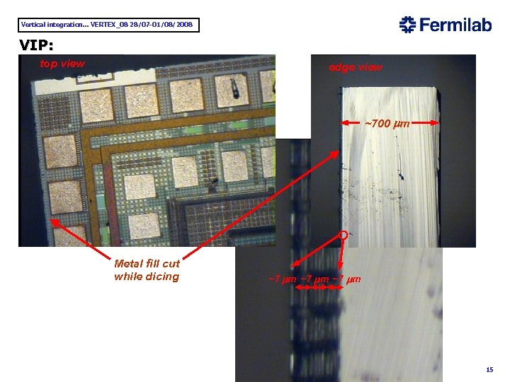 Vertical integration. . . VERTEX_08 28/07 -01/08/2008 VIP: top view edge view ~700 mm Metal fill cut while dicing ~7 mm 15
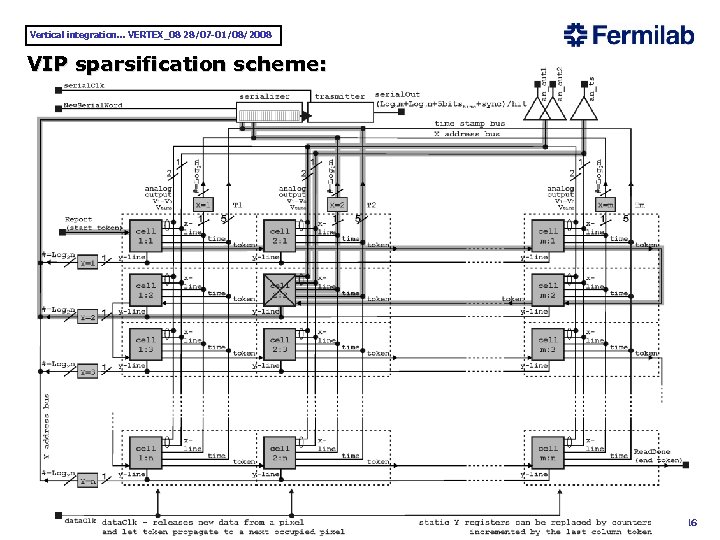 Vertical integration. . . VERTEX_08 28/07 -01/08/2008 VIP sparsification scheme: 16
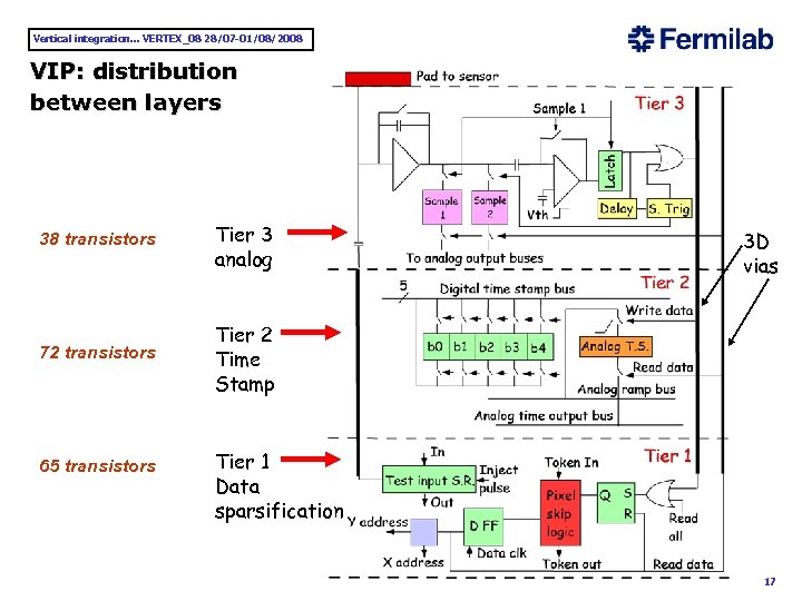 Vertical integration. . . VERTEX_08 28/07 -01/08/2008 VIP: distribution between layers 38 transistors Tier 3 analog 72 transistors Tier 2 Time Stamp 65 transistors 3 D vias Tier 1 Data sparsification 17
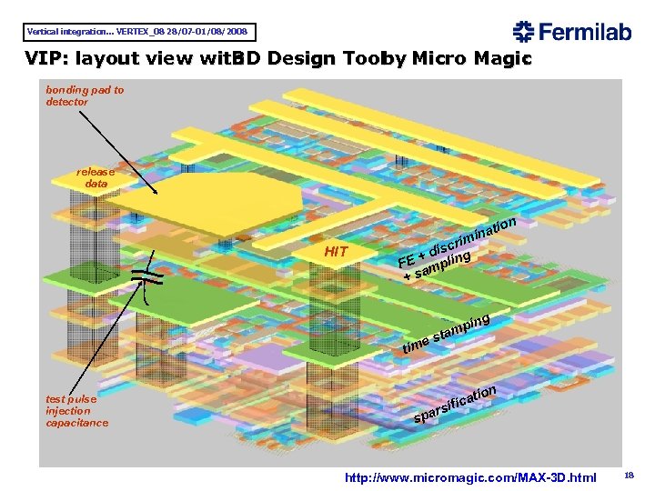 Vertical integration. . . VERTEX_08 28/07 -01/08/2008 VIP: layout view with Design Tool Micro Magic 3 D by : bonding pad to detector release data HIT ion at min cri dis ng + FE mpli a +s g in mp ta es tim test pulse injection capacitance rs spa ion at ific http: //www. micromagic. com/MAX-3 D. html 18
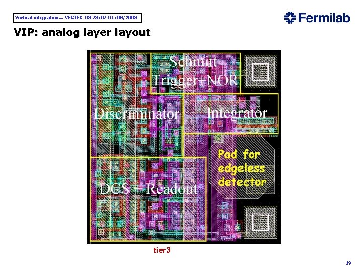 Vertical integration. . . VERTEX_08 28/07 -01/08/2008 VIP: analog layer layout tier 3 19
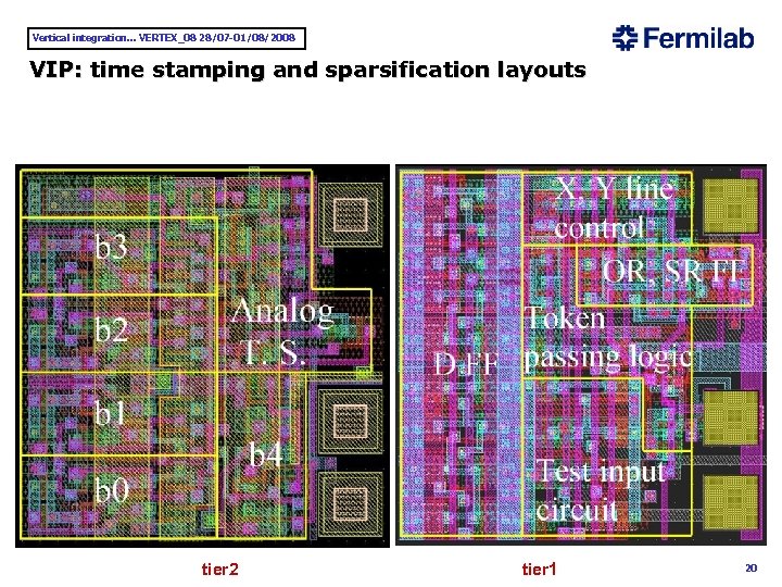 Vertical integration. . . VERTEX_08 28/07 -01/08/2008 VIP: time stamping and sparsification layouts tier 2 tier 1 20
 Vertical integration. . . VERTEX_08 28/07 -01/08/2008 Full array results: 8 poor fabrication yield: 1 testable chip among 23 tested (problem seems to be related to fabrication of individual tiers, 3 D TSV and 3 D assembly seem to be successful, 8 tests performed: - propagation of readout token, - threshold scan, - input test charge scan, - digital and analog time stamping, - full sparsified data readout, - Fixed Pattern Noise and temporal noise measurements (limited due to S/H) 8 tests used in definition of guidelines for submission of VIP 2 MIT-LL 3 DM 3 09/30/08. 21
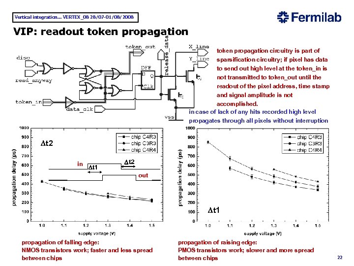 Vertical integration. . . VERTEX_08 28/07 -01/08/2008 VIP: readout token propagation circuitry is part of sparsification circuitry; if pixel has data to send out high level at the token_in is not transmitted to token_out until the readout of the pixel address, time stamp and signal amplitude is not accomplished. in case of lack of any hits recorded high level propagates through all pixels without interruption Dt 2 in Dt 1 Dt 2 out Dt 1 propagation of falling edge: NMOS transistors work; faster and less spread between chips propagation of raising edge: PMOS transistors work; slower and more spread between chips 22
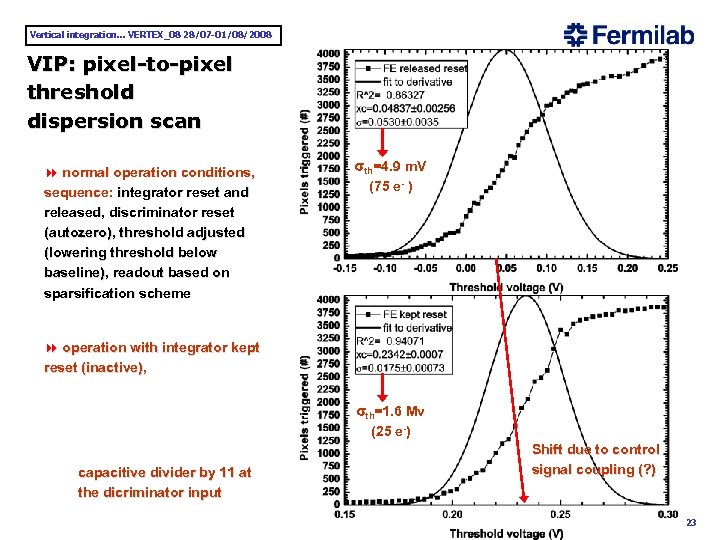 Vertical integration. . . VERTEX_08 28/07 -01/08/2008 VIP: pixel-to-pixel threshold dispersion scan 8 normal operation conditions, sequence: integrator reset and released, discriminator reset (autozero), threshold adjusted (lowering threshold below baseline), readout based on sparsification scheme sth=4. 9 m. V (75 e- ) 8 operation with integrator kept reset (inactive), sth=1. 6 Mv (25 e-) capacitive divider by 11 at the dicriminator input Shift due to control signal coupling (? ) 23
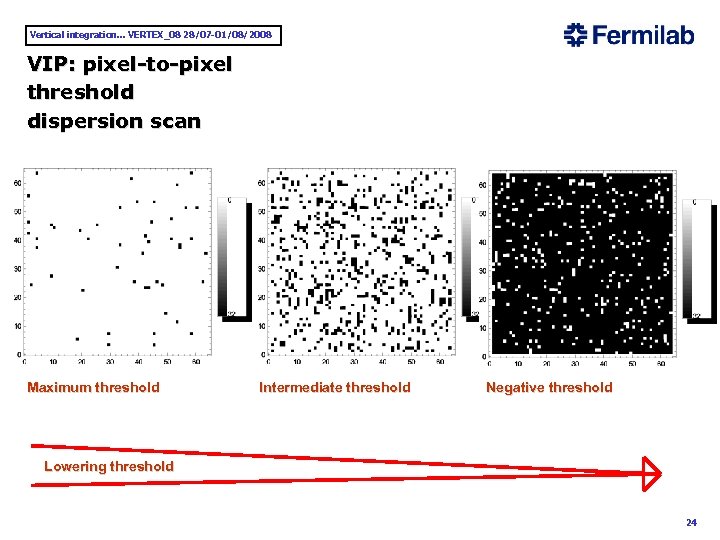 Vertical integration. . . VERTEX_08 28/07 -01/08/2008 VIP: pixel-to-pixel threshold dispersion scan Maximum threshold Intermediate threshold Negative threshold Lowering threshold 24
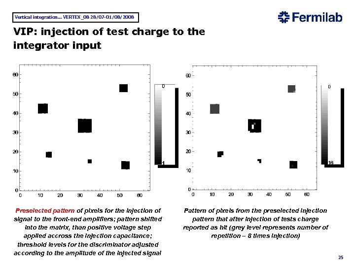 Vertical integration. . . VERTEX_08 28/07 -01/08/2008 VIP: injection of test charge to the integrator input Preselected pattern of pixels for the injection of signal to the front-end amplifiers; pattern shifted into the matrix, than positive voltage step applied accross the injection capacitance; threshold levels for the discriminator adjusted according to the amplitude of the injected signal Pattern of pixels from the preselected injection pattern that after injection of tests charge reported as hit (grey level represents number of repetition – 8 times injection) 25
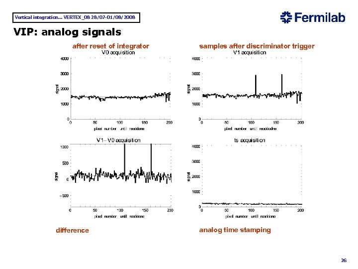 Vertical integration. . . VERTEX_08 28/07 -01/08/2008 VIP: analog signals after reset of integrator difference samples after discriminator trigger analog time stamping 26
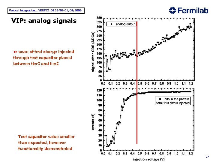 Vertical integration. . . VERTEX_08 28/07 -01/08/2008 VIP: analog signals 8 scan of test charge injected through test capacitor placed between tier 3 and tier 2 Test capacitor value smaller than expected, however functionality demonstrated 27
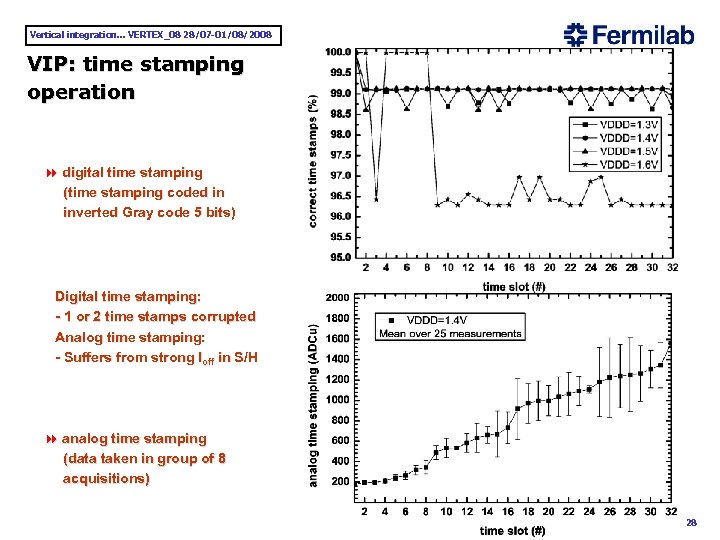 Vertical integration. . . VERTEX_08 28/07 -01/08/2008 VIP: time stamping operation 8 digital time stamping (time stamping coded in inverted Gray code 5 bits) Digital time stamping: - 1 or 2 time stamps corrupted Analog time stamping: - Suffers from strong Ioff in S/H 8 analog time stamping (data taken in group of 8 acquisitions) 28
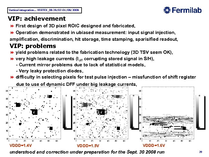 Vertical integration. . . VERTEX_08 28/07 -01/08/2008 VIP: achievement 8 First design of 3 D pixel ROIC designed and fabricated, 8 Operation demonstrated in ubiased measurement: input signal injection, amplification, discrimination, hit storage, time stamping, sparisified readout, VIP: problems 8 yield problems related to the fabrication technology (3 D TSV seem OK), 8 very high leakage currents (Ioff corrupting stored signal in S/H), - Current mirror problems due to lack of statistical models, - Very leaky protection diodes, 8 difficulty in selecting pixels for test pulse injection – missfunction of shift register due to use of dynamic DFF under big leakage currents, VDDD=1. 4 V VDDD=1. 5 V VDDD=1. 6 V understood and correction under preparation for the Sept. 30 2008 run 29
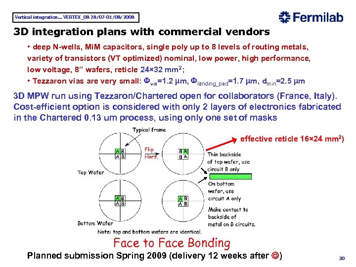 Vertical integration. . . VERTEX_08 28/07 -01/08/2008 3 D integration plans with commercial vendors • deep N-wells, Mi. M capacitors, single poly up to 8 levels of routing metals, variety of transistors (VT optimized) nominal, low power, high performance, low voltage, 8” wafers, reticle 24× 32 mm 2; • Tezzaron vias are very small: Fvia=1. 2 mm, Flanding_pad=1. 7 mm, dmin=2. 5 mm 3 D MPW run using Tezzaron/Chartered open for collaborators (France, Italy). Cost-efficient option is considered with only 2 layers of electronics fabricated in the Chartered 0. 13 um process, using only one set of masks effective reticle 16× 24 mm 2) Face to Face Bonding Planned submission Spring 2009 (delivery 12 weeks after J) 30
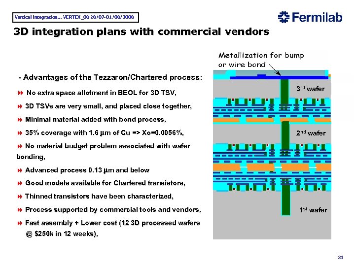 Vertical integration. . . VERTEX_08 28/07 -01/08/2008 3 D integration plans with commercial vendors - Advantages of the Tezzaron/Chartered process: 8 No extra space allotment in BEOL for 3 D TSV, 3 rd wafer 8 3 D TSVs are very small, and placed close together, 8 Minimal material added with bond process, 8 35% coverage with 1. 6 mm of Cu => Xo=0. 0056%, 2 nd wafer 8 No material budget problem associated with wafer bonding, 8 Advanced process 0. 13 mm and below 8 Good models available for Chartered transistors, 8 Thinned transistors have been characterized, 8 Process supported by commercial tools and vendors, 1 st wafer 8 Fast assembly + Lower cost (12 3 D processed wafers @ $250 k in 12 weeks), 31
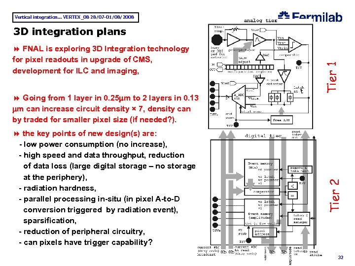 Vertical integration. . . VERTEX_08 28/07 -01/08/2008 8 Going from 1 layer in 0. 25 mm to 2 layers in 0. 13 mm can increase circuit density × 7, density can by traded for smaller pixel size (if needed? ). 8 the key points of new design(s) are: - low power consumption (no increase), - high speed and data throughput, reduction of data loss (large digital storage – no storage at the periphery), - radiation hardness, - parallel processing in-situ (in pixel A-to-D conversion triggered by radiation event), sparsification, - reduction of peripheral circuitry, - can pixels have trigger capability? Tier 2 8 FNAL is exploring 3 D Integration technology for pixel readouts in upgrade of CMS, development for ILC and imaging, Tier 1 3 D integration plans 32
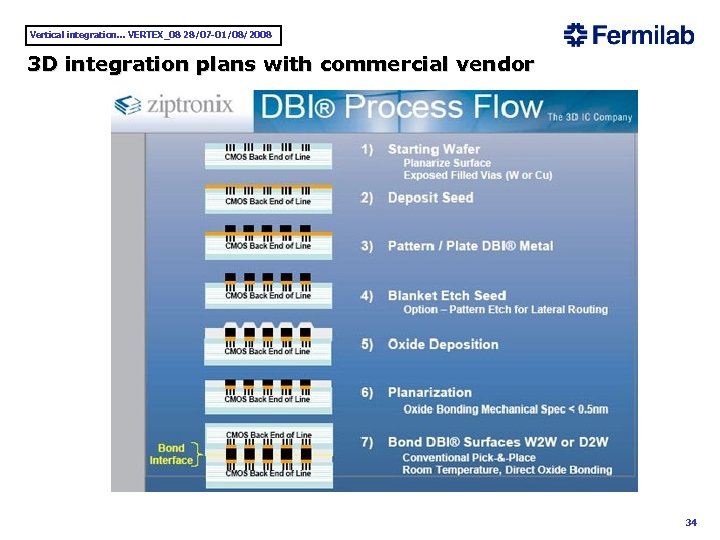
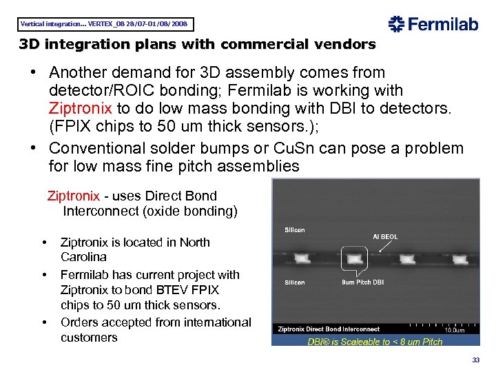 Vertical integration. . . VERTEX_08 28/07 -01/08/2008 3 D integration plans with commercial vendors • Another demand for 3 D assembly comes from detector/ROIC bonding; Fermilab is working with Ziptronix to do low mass bonding with DBI to detectors. (FPIX chips to 50 um thick sensors. ); • Conventional solder bumps or Cu. Sn can pose a problem for low mass fine pitch assemblies Ziptronix - uses Direct Bond Interconnect (oxide bonding) • • • Ziptronix is located in North Carolina Fermilab has current project with Ziptronix to bond BTEV FPIX chips to 50 um thick sensors. Orders accepted from international customers 33
 Vertical integration. . . VERTEX_08 28/07 -01/08/2008 3 D integration plans with commercial vendor 34
 Vertical integration. . . VERTEX_08 28/07 -01/08/2008 Conclusions: 8 3 D Integration is very attractive for highly granular detector systems, 8 Bonding is low temperature process, adds limited amount of high-Z material, 8 3 D-Integration may extend use of certain detector type (MAPS), 8 3 D-Integration is starting to be available in industry, 8 Commercial vendors like Tezzaron-Charted lead to lower costs, faster fabrication cycle, high yield, 8 The proposal from Fermilab, to use commercial vendors, received considerable attention and is leading to a collaboration between various groups within HEP to explore the Tezzaron 3 D process, 8 Groups in Italy, France, and the United States will be designing chips in the Tezzaron 3 D process for possible application ILC, SLHC, etc. 8 First run exploiting 3 D-Integration technology with MIT-LL (SOI based) process showed feasibility of the design, 8 One more submission in MIT-LL is envisaged, however main effort will be allocated to Tezzaron/Chartered process, 8 Dedicated EDA tools required – will our community be able to afford? 35
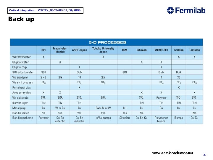 Vertical integration. . . VERTEX_08 28/07 -01/08/2008 Back up www. semiconductor. net 36


