78d57e15572f12ca4f1210b31ea5dec5.ppt
- Количество слайдов: 17
 UV Sensitive very high PDE Si. PMs with very low X-talk Razmik Mirzoyan 1, Pavel Buzhan 2, Boris Dolgoshein 2, Elena Popova 2, Masahiro Teshima 1 1 - Max-Planck-Institute for Physics, Munich, Germany 2 - National Research Nuclear University MEPh. I, Moscow, Russia
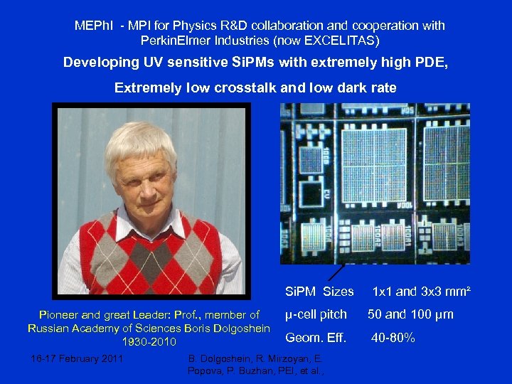 MEPh. I - MPI for Physics R&D collaboration and cooperation with Perkin. Elmer Industries (now EXCELITAS) Developing UV sensitive Si. PMs with extremely high PDE, Extremely low crosstalk and low dark rate Si. PM Sizes Pioneer and great Leader: Prof. , member of Russian Academy of Sciences Boris Dolgoshein 1930 -2010 16 -17 February 2011 1 x 1 and 3 x 3 mm² µ-cell pitch 50 and 100 µm Geom. Eff. 40 -80% B. Dolgoshein, R. Mirzoyan, E. Popova, P. Buzhan, PEI, et al. ,
 Current status of Si. PM • Currently there is a lot of enthusiasm about the new devices but the deep understanding is not simple, it comes only slowly • One of the main problems of Si. PMs is its low PDE, that is not easy to measure. It shall be disentangled from the cross-talk and after-pulsing. • The after-pulsing in PMTs is a ~1% effect on single ph. e. level, while for example, for currently existing MPPC’s from Hamamatsu it is a 20 -30 % (depending on type and the applied over-voltage) effect. • Often the real value of PDE is significantly lower than the claimed (advertised) one. The reasons are a) the low applied overvoltage, b) neglecting of the cross-talk (X-talk) and c) of the after-pulsing. Saturday 11 June 2011, TIPP-2011, Chicago R. Mirzoyan: UV sensitive high PDE, low X-talk Si. PM 3
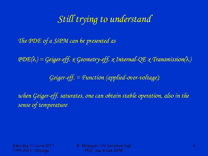 Still trying to understand The PDE of a Si. PM can be presented as PDE(l) = Geiger-eff. x Geometry-eff. x Internal-QE x Transmission( l) Geiger-eff. = Function (applied-over-voltage); when Geiger-eff. saturates, one can obtain stable operation, also in the sense of temperature Saturday 11 June 2011, TIPP-2011, Chicago R. Mirzoyan: UV sensitive high PDE, low X-talk Si. PM 4
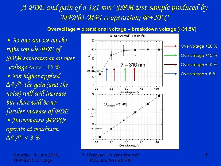 A PDE and gain of a 1 x 1 mm² Si. PM test-sample produced by MEPh. I-MPI cooperation; @+20°C Overvoltage = operational voltage – breakdown voltage (~31. 5 V) • As one can see on the right top the PDE of Si. PM saturates at an over -voltage DV/V ~15 % • For higher applied DV/V the gain (and the noise) will still increase but there will be no further increase of PDE • Hamamatsu MPPCs operate at maximum DV/V < 3 % Saturday 11 June 2011, TIPP-2011, Chicago Overvoltage +20 % Overvoltage +15 % Overvoltage +10 % Overvoltage + 5 % R. Mirzoyan: UV sensitive high PDE, low X-talk Si. PM 5
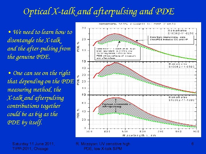 Optical X-talk and afterpulsing and PDE • We need to learn how to disentangle the X-talk and the after-pulsing from the genuine PDE. • One can see on the right that depending on the PDE measuring method, the X-talk and afterpulsing contributions together could be as big as the PDE by itself. Saturday 11 June 2011, TIPP-2011, Chicago R. Mirzoyan: UV sensitive high PDE, low X-talk Si. PM 6
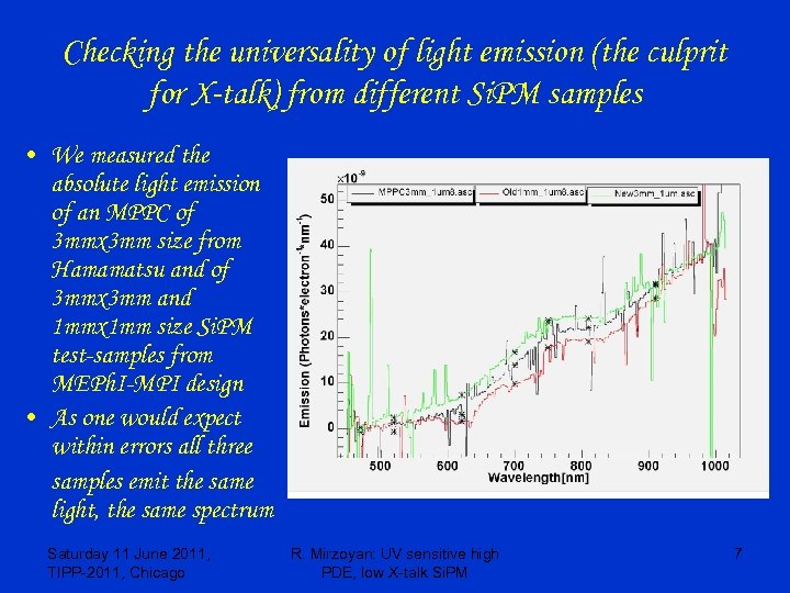 Checking the universality of light emission (the culprit for X-talk) from different Si. PM samples • We measured the absolute light emission of an MPPC of 3 mmx 3 mm size from Hamamatsu and of 3 mmx 3 mm and 1 mmx 1 mm size Si. PM test-samples from MEPh. I-MPI design • As one would expect within errors all three samples emit the same light, the same spectrum Saturday 11 June 2011, TIPP-2011, Chicago R. Mirzoyan: UV sensitive high PDE, low X-talk Si. PM 7
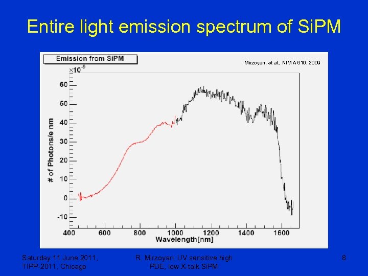 Entire light emission spectrum of Si. PM Mirzoyan, et al. , NIM A 610, 2009 Saturday 11 June 2011, TIPP-2011, Chicago R. Mirzoyan: UV sensitive high PDE, low X-talk Si. PM 8
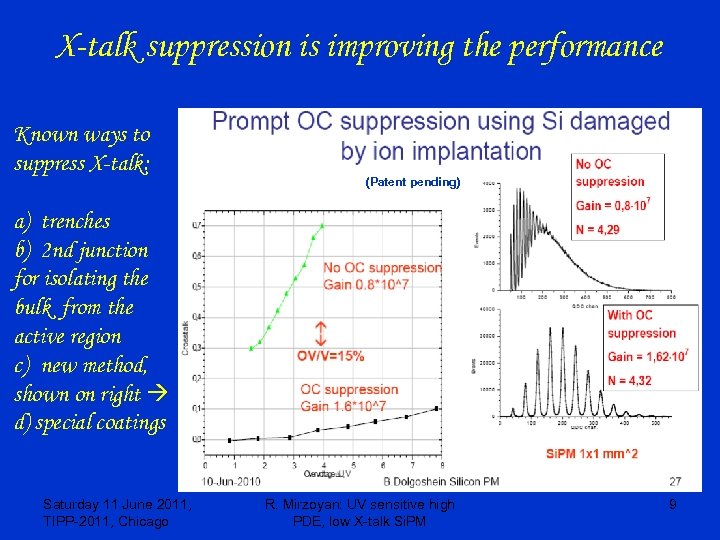 X-talk suppression is improving the performance Known ways to suppress X-talk: (Patent pending) a) trenches b) 2 nd junction for isolating the bulk from the active region c) new method, shown on right d) special coatings Saturday 11 June 2011, TIPP-2011, Chicago R. Mirzoyan: UV sensitive high PDE, low X-talk Si. PM 9
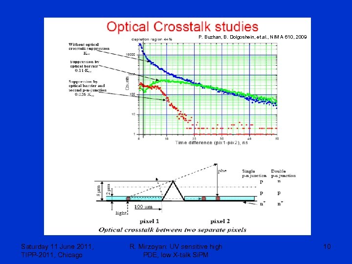 P. Buzhan, B. Dolgoshein, et al. , NIM A 610, 2009 Saturday 11 June 2011, TIPP-2011, Chicago R. Mirzoyan: UV sensitive high PDE, low X-talk Si. PM 10
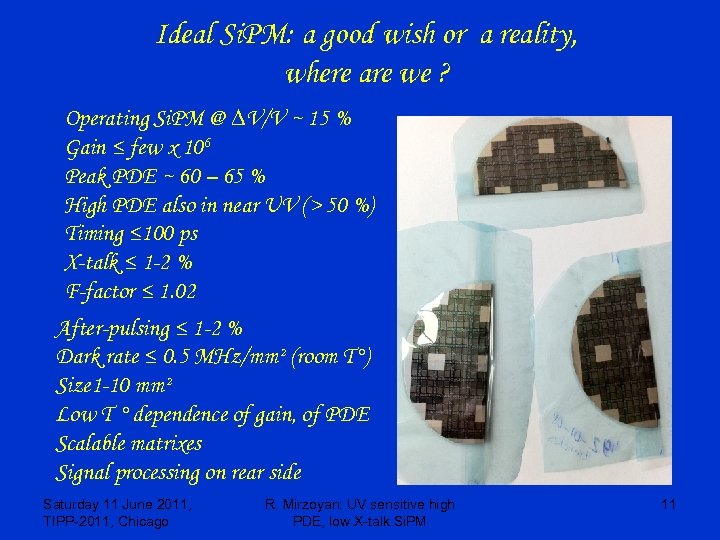 Ideal Si. PM: a good wish or a reality, where are we ? Operating Si. PM @ DV/V ~ 15 % Gain ≤ few x 106 Peak PDE ~ 60 – 65 % High PDE also in near UV (> 50 %) Timing ≤ 100 ps X-talk ≤ 1 -2 % F-factor ≤ 1. 02 After-pulsing ≤ 1 -2 % Dark rate ≤ 0. 5 MHz/mm² (room T°) Size 1 -10 mm² Low T ° dependence of gain, of PDE Scalable matrixes Signal processing on rear side Saturday 11 June 2011, TIPP-2011, Chicago R. Mirzoyan: UV sensitive high PDE, low X-talk Si. PM 11
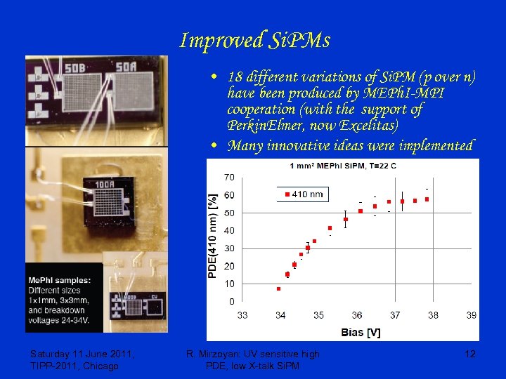 Improved Si. PMs • 18 different variations of Si. PM (p over n) have been produced by MEPh. I-MPI cooperation (with the support of Perkin. Elmer, now Excelitas) • Many innovative ideas were implemented Saturday 11 June 2011, TIPP-2011, Chicago R. Mirzoyan: UV sensitive high PDE, low X-talk Si. PM 12
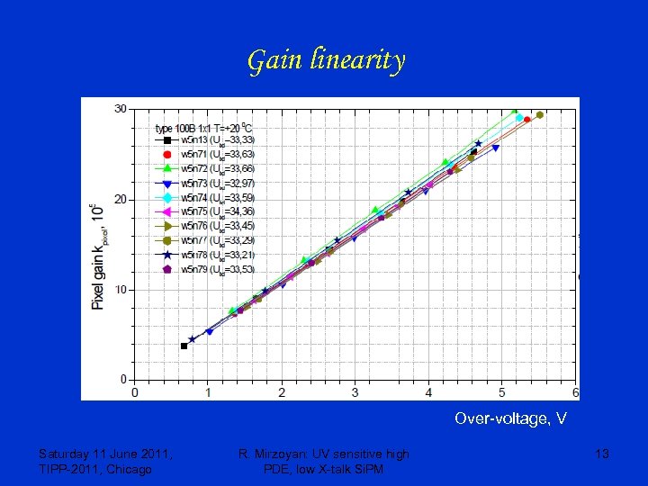 Gain linearity Over-voltage, V Saturday 11 June 2011, TIPP-2011, Chicago R. Mirzoyan: UV sensitive high PDE, low X-talk Si. PM 13
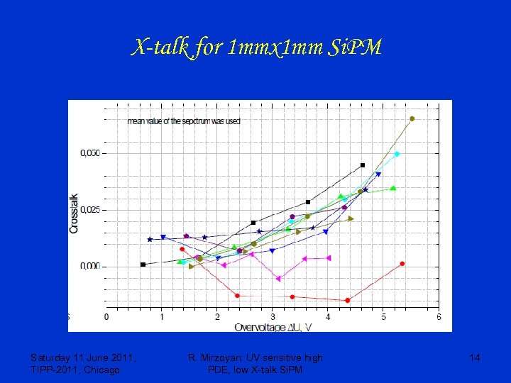 X-talk for 1 mmx 1 mm Si. PM Saturday 11 June 2011, TIPP-2011, Chicago R. Mirzoyan: UV sensitive high PDE, low X-talk Si. PM 14
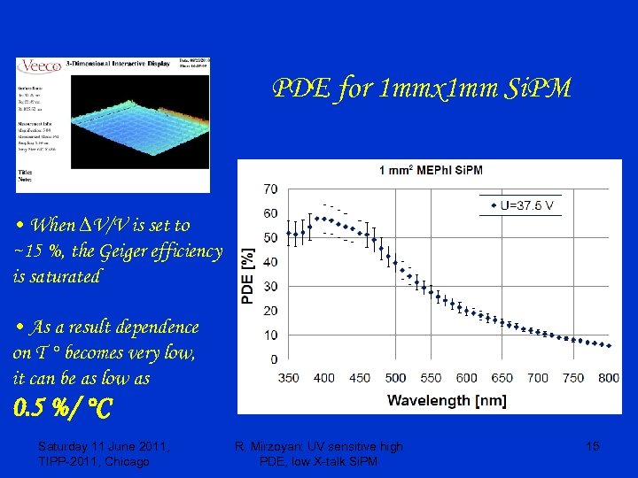 PDE for 1 mmx 1 mm Si. PM • When DV/V is set to ~15 %, the Geiger efficiency is saturated • As a result dependence on T ° becomes very low, it can be as low as 0. 5 %/ °C Saturday 11 June 2011, TIPP-2011, Chicago R. Mirzoyan: UV sensitive high PDE, low X-talk Si. PM 15
 Conclusions • In a time scale of 1 -2 years from now one can buy Si. PMs with really outstanding characteristics, probably from several manufacturers. • Their sizes could span 1 -10 mm (in remote future perhaps even larger) • Si. PM cost will be reduced due to the availability of full CMOS designs. Several USD per mm² is not very unrealistic. • These devices are going to substitute classical PMTs and APD in many (but of course not all) applications, including those in physics instrumentation in, for example, nuclear medicine (time-of-flight PET, …). • We could demonstrate samples with max. PDE of 50 -60 %, X-talk in the range of < 2 -5 % and a very high PDE also in the UV when operated at ~15 % over-voltage Saturday 11 June 2011, TIPP-2011, Chicago R. Mirzoyan: UV sensitive high PDE, low X-talk Si. PM 16
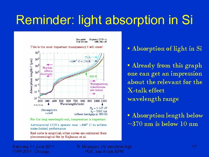 Reminder: light absorption in Si • Absorption of light in Si • Already from this graph one can get an impression about the relevant for the X-talk effect wavelength range • Absorption length below ~370 nm is below 10 nm Saturday 11 June 2011, TIPP-2011, Chicago R. Mirzoyan: UV sensitive high PDE, low X-talk Si. PM 17


