3d9d76739af692be4bed6efc14cd6cba.ppt
- Количество слайдов: 37
 Un/Do. Pack: Re-Clustering of Large System-on-Chip Designs with Interconnect Variation for Low-Cost FPGAs Marvin Tom* Xilinx Inc. (marvin. tom@xilinx. com) San Jose, CA, USA *Work performed at University of British Columbia David Leong University of British Columbia (davel@ece. ubc. ca) Vancouver, BC, Canada Guy Lemieux University of British Columbia (lemieux@ece. ubc. ca) Vancouver, BC, Canada
 Overview • Introduction, Goals and Motivation – Reduce channel width, lower cost, make circuits “routable” • Benchmark Circuits – Varying amount of interconnect variation • Un/Do. Pack CAD Tool: – Iterative channel width reduction by whitespace insertion • Results • Conclusion 2
 Overview • Introduction, Goals and Motivation – Reduce channel width, lower cost, make circuits “routable” • Benchmark Circuits – Varying amount of interconnect variation • Un/Do. Pack CAD Tool: – Iterative channel width reduction by whitespace insertion • Results • Conclusion 3
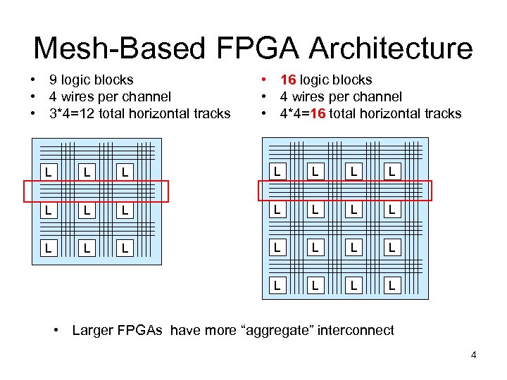 Mesh-Based FPGA Architecture • 9 logic blocks • 4 wires per channel • 3*4=12 total horizontal tracks • 16 logic blocks • 4 wires per channel • 4*4=16 total horizontal tracks L L L L L L L • Larger FPGAs have more “aggregate” interconnect 4
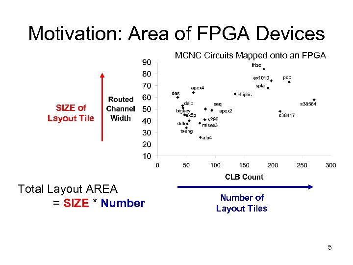 Motivation: Area of FPGA Devices MCNC Circuits Mapped onto an FPGA SIZE of Layout Tile Total Layout AREA = SIZE * Number of Layout Tiles 5
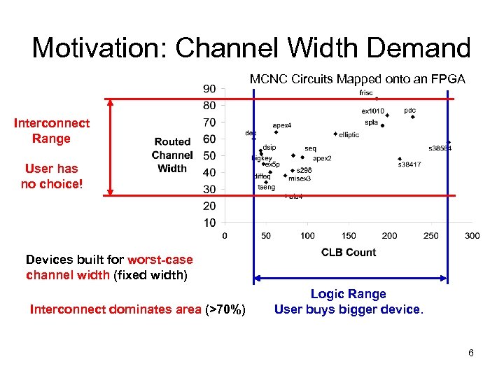 Motivation: Channel Width Demand MCNC Circuits Mapped onto an FPGA Interconnect Range User has no choice! Devices built for worst-case channel width (fixed width) Interconnect dominates area (>70%) Logic Range User buys bigger device. 6
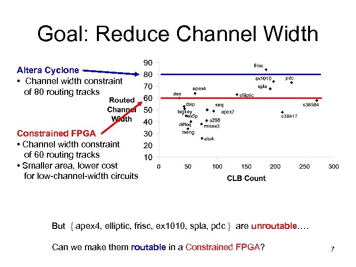 Goal: Reduce Channel Width Altera Cyclone • Channel width constraint of 80 routing tracks Constrained FPGA • Channel width constraint of 60 routing tracks • Smaller area, lower cost for low-channel-width circuits But { apex 4, elliptic, frisc, ex 1010, spla, pdc } are unroutable…. Can we make them routable in a Constrained FPGA? 7
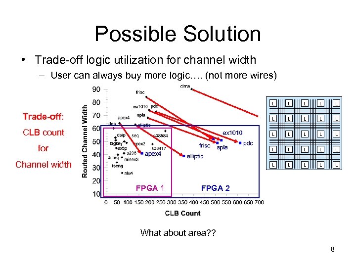 Possible Solution • Trade-off logic utilization for channel width – User can always buy more logic…. (not more wires) L L L L Trade-off: L L L L CLB count L L L L L for L L L L L Channel width L L L FPGA 1 FPGA 2 What about area? ? 8
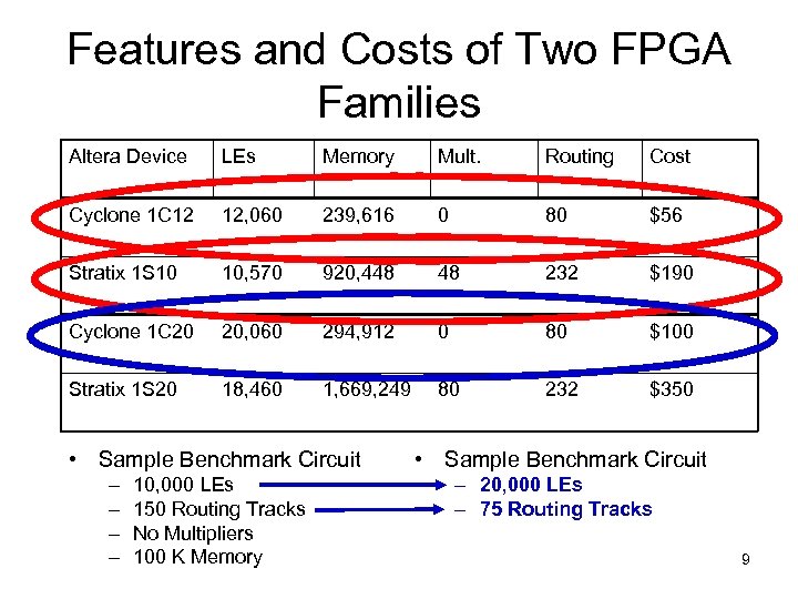 Features and Costs of Two FPGA Families Altera Device LEs Memory Mult. Routing Cost Cyclone 1 C 12 12, 060 239, 616 0 80 $56 Stratix 1 S 10 10, 570 920, 448 48 232 $190 Cyclone 1 C 20 20, 060 294, 912 0 80 $100 Stratix 1 S 20 18, 460 1, 669, 249 80 232 $350 • Sample Benchmark Circuit – – 10, 000 LEs 150 Routing Tracks No Multipliers 100 K Memory • Sample Benchmark Circuit – 20, 000 LEs – 75 Routing Tracks 9
 Overview • Introduction, Goals and Motivation – Reduce channel width, lower cost, make circuits “routable” • Benchmark Circuits – Varying amount of interconnect variation • Un/Do. Pack CAD Tool: – Iterative channel width reduction by whitespace insertion • Results • Conclusion 10
 GNL Circuit Benchmark Suite • Create benchmark circuits with variation – So. C <==> Randomly integrate/stitch together “IP Blocks” – IP Blocks have varied interconnect needs • Generate Netlist (GNL) – Stroobandt @ Ghent University – Synthetic benchmark generator • GNL circuits generated hierarchically – Root # I/Os, # IP blocks – Second Level 20 IP blocks, # LEs, Rent parameter 11
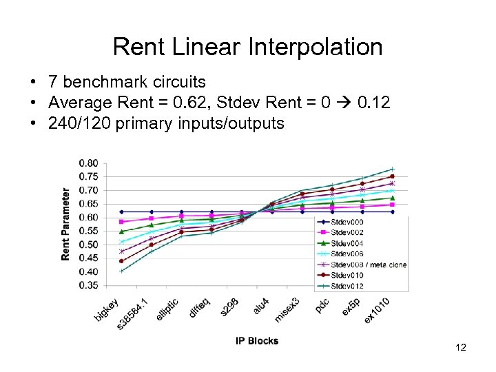 Rent Linear Interpolation • 7 benchmark circuits • Average Rent = 0. 62, Stdev Rent = 0 0. 12 • 240/120 primary inputs/outputs 12
 Overview • Introduction, Goals and Motivation – Reduce channel width, lower cost, make circuits “routable” • Benchmark Circuits – Varying amount of interconnect variation • Un/Do. Pack CAD Tool: – Iterative channel width reduction by whitespace insertion • Results • Conclusion 13
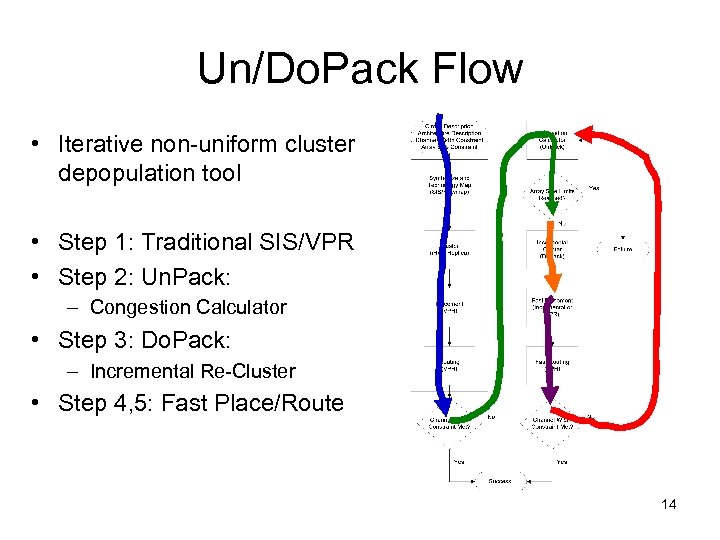 Un/Do. Pack Flow • Iterative non-uniform cluster depopulation tool • Step 1: Traditional SIS/VPR • Step 2: Un. Pack: – Congestion Calculator • Step 3: Do. Pack: – Incremental Re-Cluster • Step 4, 5: Fast Place/Route 14
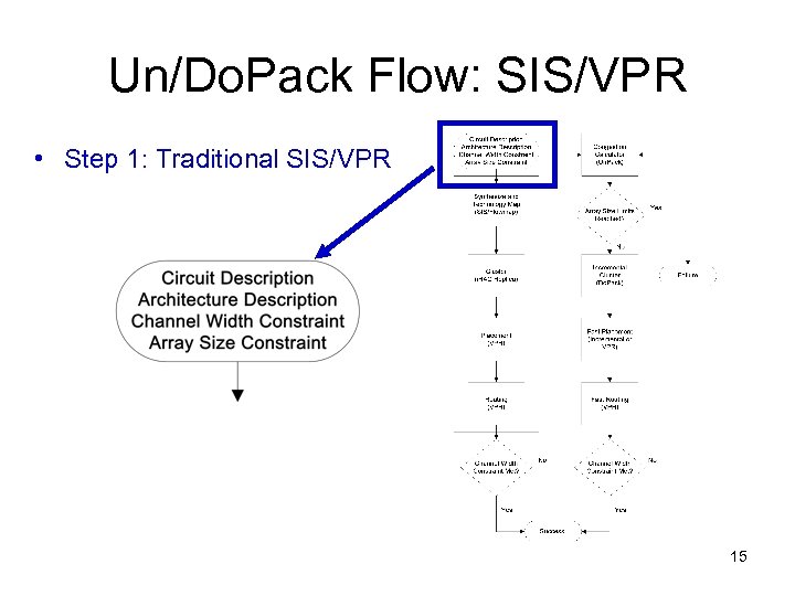 Un/Do. Pack Flow: SIS/VPR • Step 1: Traditional SIS/VPR 15
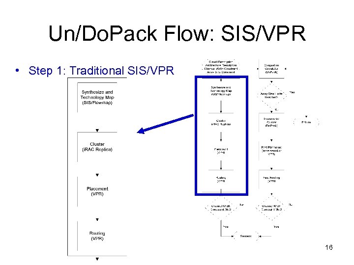 Un/Do. Pack Flow: SIS/VPR • Step 1: Traditional SIS/VPR 16
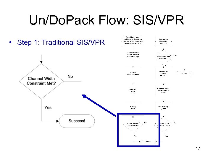 Un/Do. Pack Flow: SIS/VPR • Step 1: Traditional SIS/VPR 17
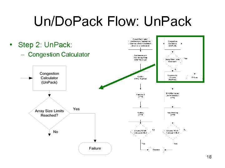 Un/Do. Pack Flow: Un. Pack • Step 2: Un. Pack: – Congestion Calculator 18
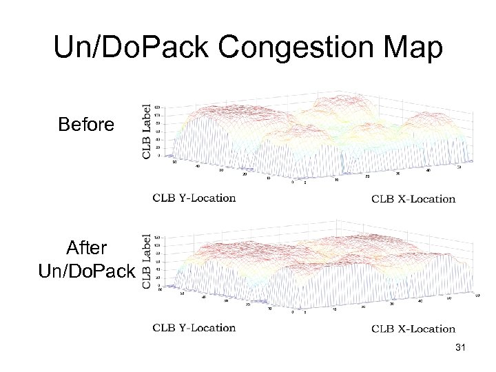
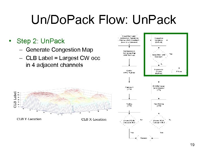 Un/Do. Pack Flow: Un. Pack • Step 2: Un. Pack – Generate Congestion Map – CLB Label = Largest CW occ in 4 adjacent channels 19
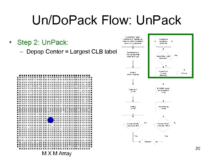 Un/Do. Pack Flow: Un. Pack • Step 2: Un. Pack: – Depop Center = Largest CLB label M X M Array 20
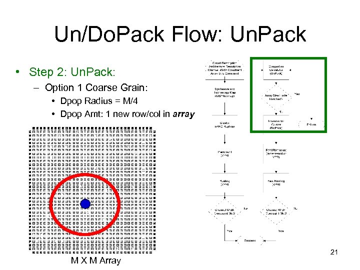 Un/Do. Pack Flow: Un. Pack • Step 2: Un. Pack: – Option 1 Coarse Grain: • Dpop Radius = M/4 • Dpop Amt: 1 new row/col in array M X M Array 21
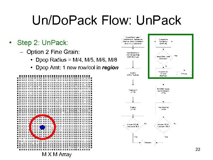 Un/Do. Pack Flow: Un. Pack • Step 2: Un. Pack: – Option 2 Fine Grain: • Dpop Radius = M/4, M/5, M/6, M/8 • Dpop Amt: 1 new row/col in region M X M Array 22
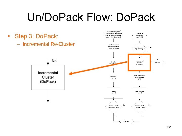 Un/Do. Pack Flow: Do. Pack • Step 3: Do. Pack: – Incremental Re-Cluster 23
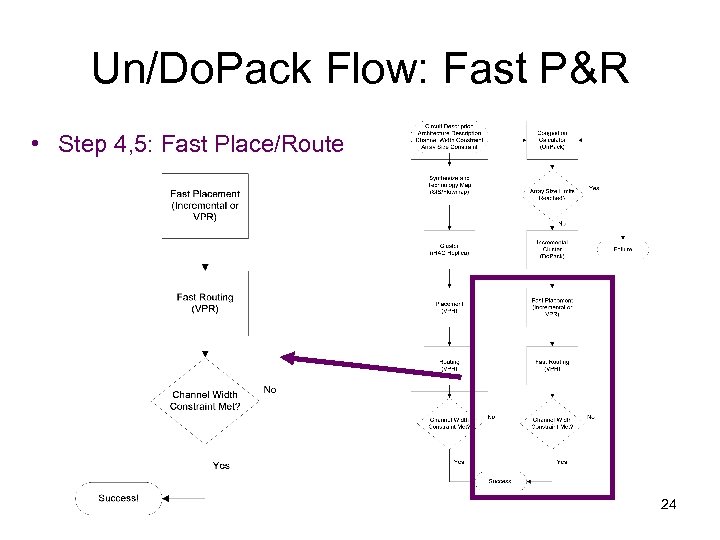 Un/Do. Pack Flow: Fast P&R • Step 4, 5: Fast Place/Route 24
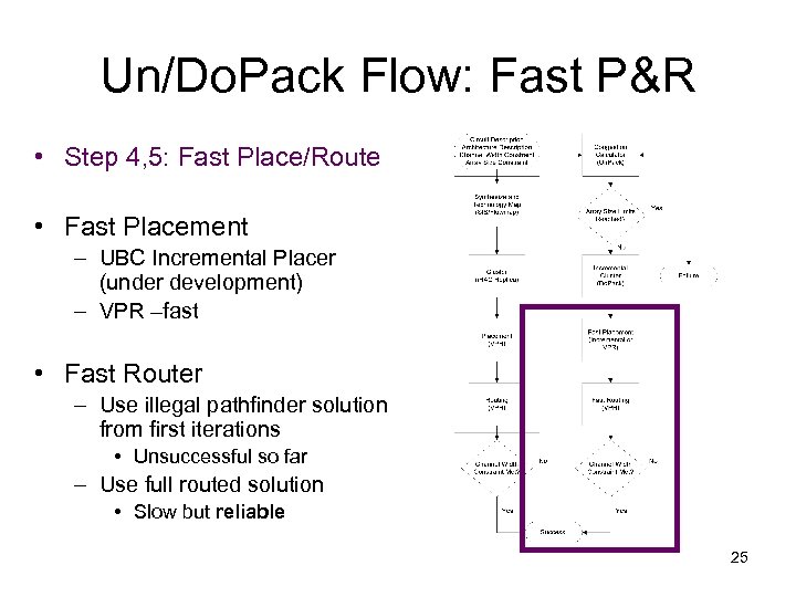 Un/Do. Pack Flow: Fast P&R • Step 4, 5: Fast Place/Route • Fast Placement – UBC Incremental Placer (under development) – VPR –fast • Fast Router – Use illegal pathfinder solution from first iterations • Unsuccessful so far – Use full routed solution • Slow but reliable 25
 Overview • Introduction, Goals and Motivation – Reduce channel width, lower cost, make circuits “routable” • Benchmark Circuits – Varying amount of interconnect variation • Un/Do. Pack CAD Tool: – Iterative channel width reduction by whitespace insertion • Results • Conclusion 26
 Un/Do. Pack: Baseline Flow • • Un. Pack: Coarse grained congestion calculator Do. Pack: i. RAC replica Fast Place: UBC Incremental Placer Fast Route: None • FPGA Architecture: – – LUT size (k) = 6 Cluster size (N) = 16 Inputs per cluster (I) = 51 Wires of length (L) = 4 27
 Area of GNL Benchmarks 28
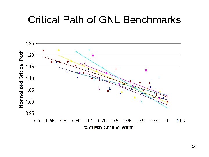
 Interconnect Variation: Impact on FPGA Architecture Design High Variation Circuits Require Wide Channel Width 29
 Critical Path of GNL Benchmarks 30
 Un/Do. Pack Congestion Map Before After Un/Do. Pack 31
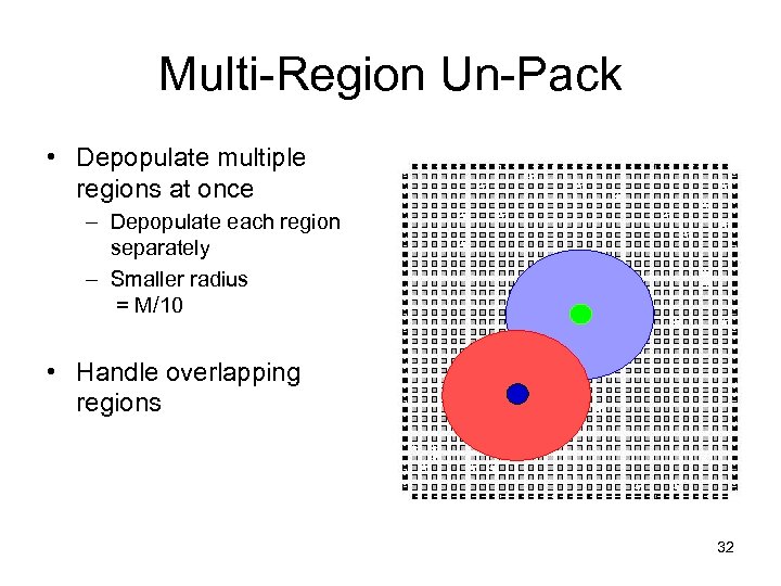 Multi-Region Un-Pack • Depopulate multiple regions at once – Depopulate each region separately – Smaller radius = M/10 • Handle overlapping regions 32
 Normalized Area 33
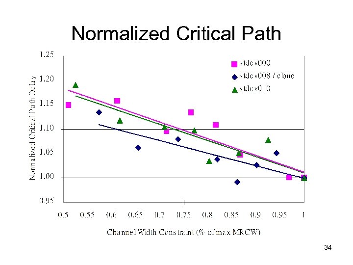 Normalized Critical Path 34
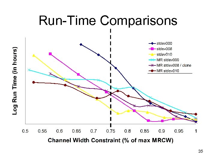 Run-Time Comparisons 35
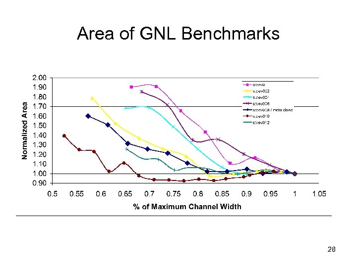
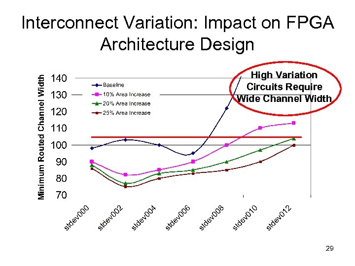
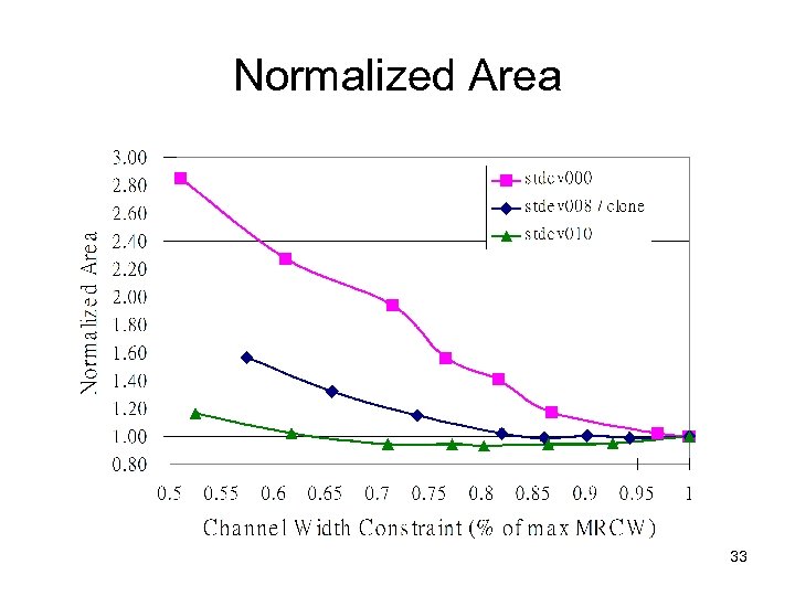
 Conclusion • Un/Do. Pack: FPGA CAD flow – Find “local” congestion depopulate reduced interconnect demand • FPGA benchmark circuit “suite” – Stdev: Used to vary interconnect demand • Discoveries… – “Non-uniform” depopulation limits area inflation – “Interconnect variation” important for area inflation and FPGA architecture design – “Routing closure” achieved by re-clustering and incremental place & route • UNROUTABLE circuits made ROUTABLE buy an FPGA with MORE LOGIC!!! 36
 End of Talk


