8a01ca15465104b8c7a8a15e8fe24f6a.ppt
- Количество слайдов: 54
 UK Si. Ge Research Programme Review Meeting, 3 rd April, 2003 Advanced Silicon/Silicon-Germanium Device Simulations John Barker in collaboration with Asenov, Mirela Borici, Scott Roy, Jeremy Watling, Richard Wilkins, Lianfeng Yang Nanoelectronics Research Centre Department of Electronics and Electrical Engineering University of Glasgow
 Outline • Is silicon near its end? • Physics, Modelling and Simulation • Interface Roughness • Silicon-Germanium studies • Advanced Simulation methodology • Advanced Devices • Fully quantum atomistic simulation • Summary
 1. Is silicon near its end? 1978: red brick wall 0. 25µm limit, alternatives included magnetic bubble logic conv. & quantum devices based on Ga. As and In. P! House of Commons Select Committee (2002) Red brick wall between 2005 -2007 Fundamental limit: 2015 Theory Limit: 10 -20 nm Suggests: single electronics, magnetic and atomic devices carbon nanotubes, quantum computing and other radical alternatives to CMOS be pursued Concentrate on microprocessor design and architecture
 Atomic scale MOSFET in the near future ? ? We still firmly believe the Si route is the best
 Reality check: Scaling of MOSFETs to decanano dimensions House of Lords The accelerating road map!
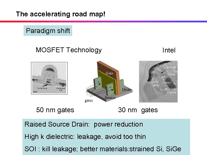 The accelerating road map! Paradigm shift MOSFET Technology 50 nm gates Intel 30 nm gates Raised Source Drain: power reduction High k dielectric: leakage, avoid too thin SOI : kill leakage; better materials: strained Si, Si. Ge
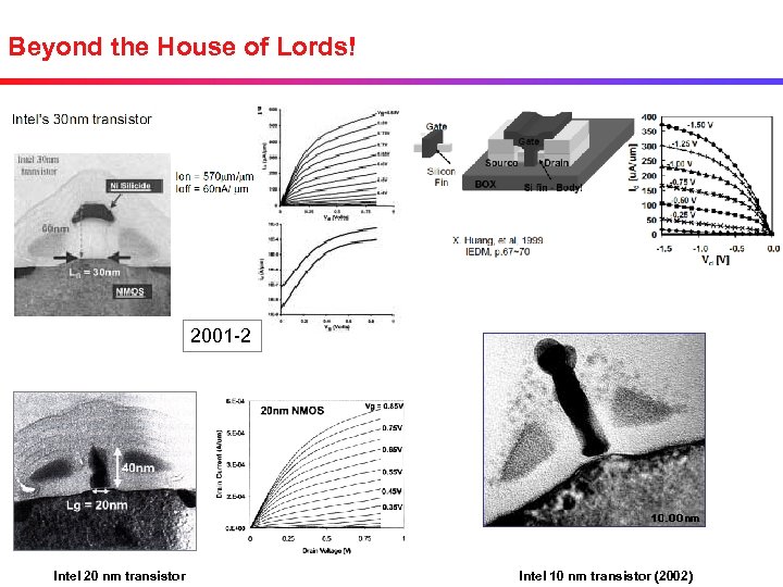 Beyond the House of Lords! 2001 -2 Intel 20 nm transistor Intel 10 nm transistor (2002)
 The IBM 6 nm silicon transistor (IEDM 2002) demonstrated
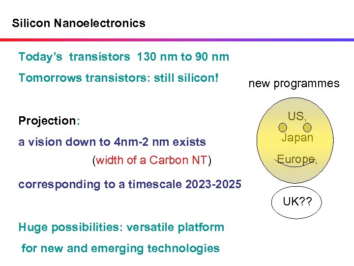 Silicon Nanoelectronics Today’s transistors 130 nm to 90 nm Tomorrows transistors: still silicon! new programmes US, Projection: a vision down to 4 nm-2 nm exists (width of a Carbon NT) Japan Europe, corresponding to a timescale 2023 -2025 UK? ? Huge possibilities: versatile platform for new and emerging technologies
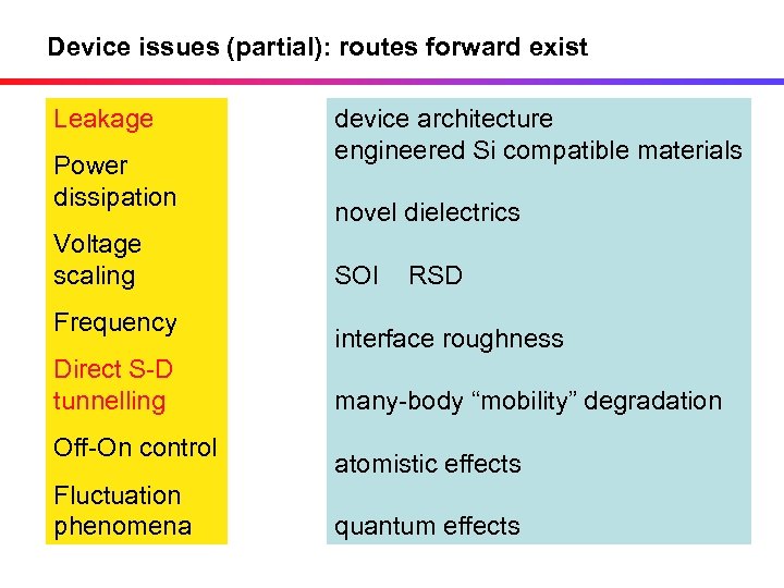 Device issues (partial): routes forward exist Leakage Power dissipation Voltage scaling Frequency Direct S-D tunnelling Off-On control Fluctuation phenomena device architecture engineered Si compatible materials novel dielectrics SOI RSD interface roughness many-body “mobility” degradation atomistic effects quantum effects
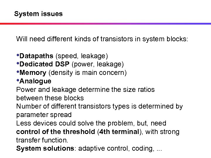 System issues Will need different kinds of transistors in system blocks: • Datapaths (speed, leakage) • Dedicated DSP (power, leakage) • Memory (density is main concern) • Analogue Power and leakage determine the size ratios between these blocks Number of different transistors types is determined by parameter spread Less devices could solve the problem, but, need control of the threshold (4 th terminal), with strong transfer function. System solutions: adaptive control, coding, . . .
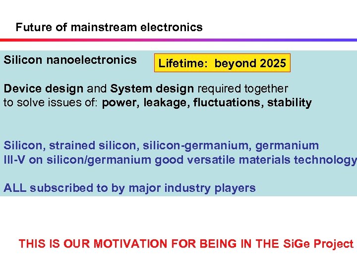 Future of mainstream electronics Silicon nanoelectronics Lifetime: beyond 2025 Device design and System design required together to solve issues of: power, leakage, fluctuations, stability Silicon, strained silicon, silicon-germanium, germanium III-V on silicon/germanium good versatile materials technology ALL subscribed to by major industry players THIS IS OUR MOTIVATION FOR BEING IN THE Si. Ge Project
 2. Physics, modelling and simulation Why is simulation useful? • Part of the design-optimisation cycle • Extraction of circuit parameters • Calibration and extension of commercial tools • Develop device physics and architecture • Getting ahead of the game.
 Summary of Progress (2002 -2003) - see also posters Simulation tools Development of a fully bipolar (electrons and holes) 2 -D Full-Band Monte Carlo device simulator for Si/strained Si/Si. Ge that includes degeneracy, high doping effects, advanced screening potential models, quantum 30 nm. Device Physics and new Simulation tools – – – Investigation of carrier transport and scattering at interfaces New non-perturbative models for interface roughness scattering Effects of degeneracy, high doping, band-gap narrowing Advanced screening models Quantum transport extensions: density gradient, quantum potential, Wigner function, Green function Atomistic studies: classical , semi-classical and full quantum transport Design - optimisation with partners – – Layer and device design for consortium partners Modelling and scaling study of high linearity MODFETs, based on experimental data from Daimler Chrysler Applications to partners and industry Si. Ge MODFETs, RF devices, Si, strained Si and Si. Ge well tempered devices, double gate devices, atomistic devices. Course on Device Modelling
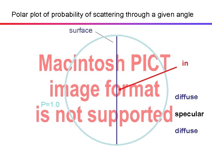
 4. Interface Roughness: new non-perturbative model • An extension of semi-classical Boltzmann-Fuchs theory, that is suitable for efficient inclusion within the Monte Carlo framework. • Probability of specular or diffuse scattering is chosen according to the carrier k-vector and incident scattering angle. This overcomes one of the major failings of the traditional semi-classical model. The scattering from a rough surface, has strong randomizing effects, resulting in a broad distribution over the emergent angles, while scattering from a smoother interface has a high probability at emergent angles close to specular
 Diffuse scattering, depends on the autocorrelation function considered. Gaussian auto-covariance RMS height: 0. 5 nm 3 nm Exponential auto-covariance Correlation Length: Lc =
 Polar plot of probability of scattering through a given angle surface in P=1. 0 diffuse specular diffuse
 Semi-classical model versus ab-initio quantum calculations
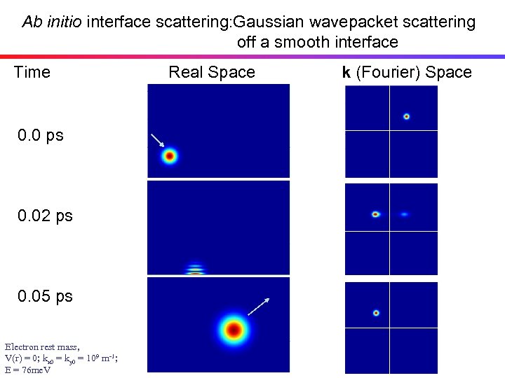 Ab initio interface scattering: Gaussian wavepacket scattering off a smooth interface Time Real Space 0. 0 ps Initial Motion of Wave Packet 0. 02 ps 0. 05 ps Electron rest mass, V(r) = 0; kx 0 = ky 0 = 109 m-1; E = 76 me. V k (Fourier) Space
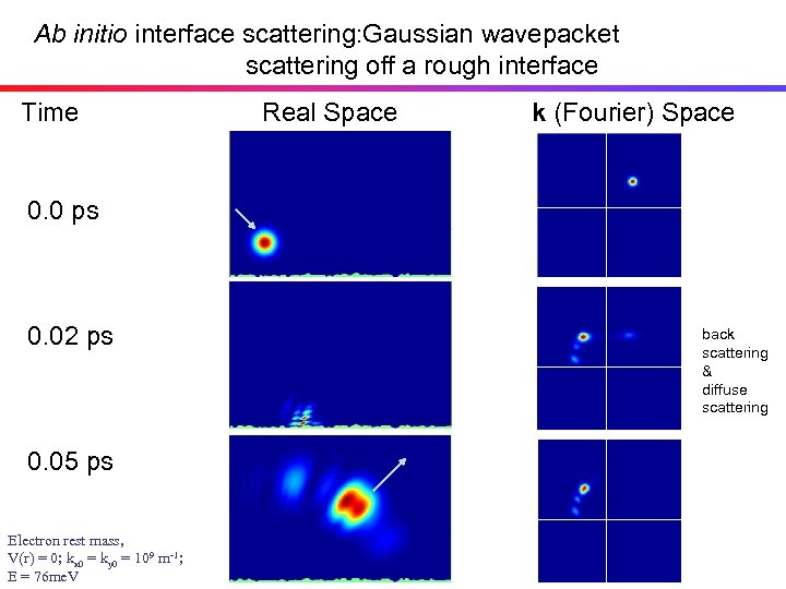 Ab initio interface scattering: Gaussian wavepacket scattering off a rough interface Time Real Space k (Fourier) Space 0. 0 ps Initial Motion of Wave Packet 0. 02 ps 0. 05 ps Electron rest mass, V(r) = 0; kx 0 = ky 0 = 109 m-1; E = 76 me. V back scattering & diffuse scattering
 4. Silicon-Germanium Studies: 2 examples • Simulation of 67 nm IBM Relaxed and Strained Si n-MOSFET. Provides test for interface roughness simulations • Optimizations of Si/Si. Ge 70 nm MODFET for RF and high linearity applications: using Daimler-Chrysler data (part of support for experimental RF and linear systems programme) Other work: see posters
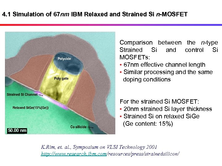 4. 1 Simulation of 67 nm IBM Relaxed and Strained Si n-MOSFET Comparison between the n-type Strained Si and control Si MOSFETs: • 67 nm effective channel length • Similar processing and the same doping conditions For the strained Si MOSFET: • 20 nm strained Si layer thickness • Strained Si on relaxed Si. Ge (Ge content: 15%) K. Rim, et. al. , Symposium on VLSI Technology 2001 http: //www. research. ibm. com/resources/press/strainedsilicon/
 Id-Vg Current Characteristics: Monte Carlo v Experiment
 Id-Vg Current Characteristics (higher fields)
 Channel Velocities: Monte Carlo Electron Velocities along the channel of IBM 67 nm Si n-MOSFET, V =V =1 V
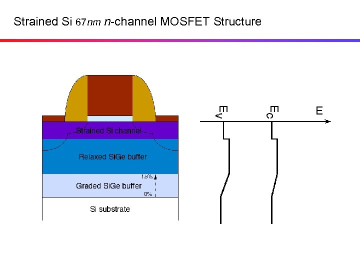 Strained Si 67 nm n-channel MOSFET Structure
 Id-Vg Current Characteristics for strained Si n-MOSFET
 Study 2: Optimizations of Si/Si. Ge MODFET for RF and high linearity applications • Based on the understanding of a Daimler-Chrysler 70 nm Si/Si. Ge MODFET • Aim for high RF performance and high linearity: • RF: f. T=f(gm, Cg, etc); fmax=f(f. T, gm, Cgs, Cgd, gds, etc) • Linearity: PIP 3=4 gm/(gm 2 RL) High is Good • Trade-off designs between f. T and linearity • Gate-to-channel distance • Gate position (Lgs/Lds) • Doping in the channel (MODFETs vs. DCFETs) • Effects of scaling on RF performance and linearity L. Yang, A. Asenov, M. Boriçi, J. R. Watling, J. R. Barker, S. Roy, K. Elgaid 1, I. Thayne, T. Hackbarth
 Device Structure • MODFET • Daimler. Chrysler structure • double-side modulation doping • high mobility • MODFET with doped channel • sandwich-like doped channel • reduced mobility • high carrier density • Doped Channel FET (DCFET) • sandwich-like doped channel • without modulation doping • high carrier density • lower mobility
 Calibrations of drift-diffusion simulators Calibrated Id-Vg characteristics of Daimler. Chrysler 70 nm Si/Si. Ge MODFET
 One example: Effects of the gate-to-channel distance small d is worst for linearity but good for RF Effects of the gate-to-channel distance d on the linearity (PIP 3); the inset is the effect of d on the transconductance gm
 Results • Trade-off designs for RF performance and linearity • Gate-to-channel distance d: decreasing d enhances RF, but lowers linearity • Gate position Lgs/Lds: increasing Lgs/Lds achieves high linearity, but reduces gm and drive current ID • Doped channel – leads to good linearity, although gives a decrease for gm and drive current ID • Scaling • improved RF performance • slightly decreased linearity
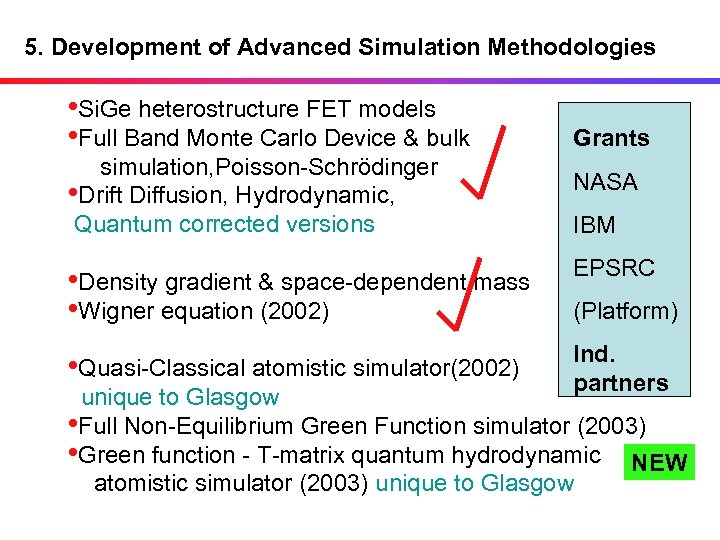 5. Development of Advanced Simulation Methodologies • Si. Ge heterostructure FET models • Full Band Monte Carlo Device & bulk simulation, Poisson-Schrödinger • Drift Diffusion, Hydrodynamic, Quantum corrected versions Grants NASA IBM • Density gradient & space-dependent mass • Wigner equation (2002) EPSRC • Quasi-Classical atomistic simulator(2002) Ind. partners (Platform) unique to Glasgow • Full Non-Equilibrium Green Function simulator (2003) • Green function - T-matrix quantum hydrodynamic NEW atomistic simulator (2003) unique to Glasgow
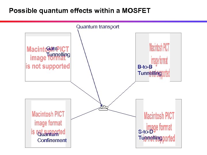 Possible quantum effects within a MOSFET Quantum transport Gate Tunnelling B-to-B Tunnelling Quantum Confinement S-to-D Tunnelling
 6. Advanced Devices • • Intel have announced conventional MOSFETs scaled down to 10 nm, and IBM have even announced a 6 nm channel length. The scaling of this design below 10 nm is likely to require intolerably thin gate oxides and unacceptably high channel doping, therefore advocating a departure from the conventional MOSFET concept. 4 nm Double gate MOSFET: An Artist’s Impression • One of the most promising new device structures is the doublegate MOSFET, with the possibility of scaling to 10 nm and below, where direct source-drain tunnelling will become a real possibility.
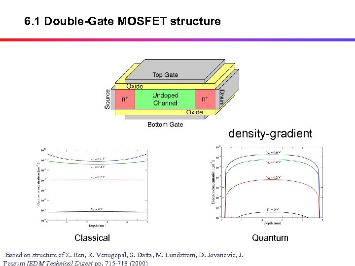 6. 1 Double-Gate MOSFET structure density-gradient Classical Based on structure of Z. Ren, R. Venugopal, S. Datta, M. Lundstrom, D. Jovanovic, J. Fossum IEDM Technical Digest pp. 715 -718 (2000) Quantum
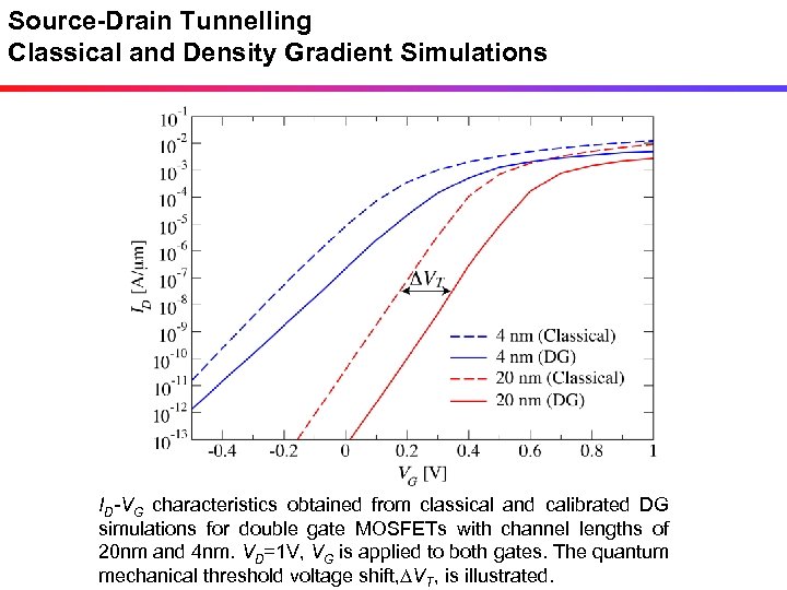 Source-Drain Tunnelling Classical and Density Gradient Simulations ID-VG characteristics obtained from classical and calibrated DG simulations for double gate MOSFETs with channel lengths of 20 nm and 4 nm. VD=1 V, VG is applied to both gates. The quantum mechanical threshold voltage shift, VT, is illustrated.
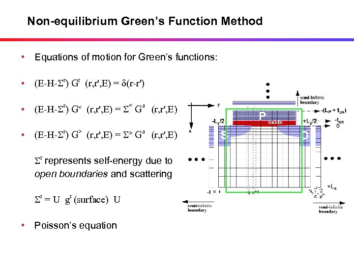 Non-equilibrium Green’s Function Method • Equations of motion for Green’s functions: • (E-H-Sr) Gr (r, r', E) = d(r-r') • (E-H-Sr) G< (r, r', E) = S< Ga (r, r', E) • (E-H-Sr) G> (r, r', E) = S> Ga (r, r', E) Sr represents self-energy due to open boundaries and scattering Sr = U gr (surface) U • Poisson’s equation
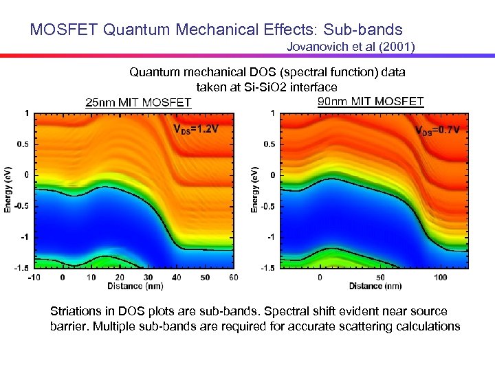 MOSFET Quantum Mechanical Effects: Sub-bands Jovanovich et al (2001) Quantum mechanical DOS (spectral function) data taken at Si-Si. O 2 interface Striations in DOS plots are sub-bands. Spectral shift evident near source barrier. Multiple sub-bands are required for accurate scattering calculations
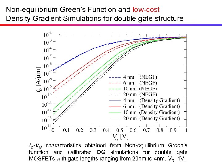 Non-equilibrium Green’s Function and low-cost Density Gradient Simulations for double gate structure ID-VG characteristics obtained from Non-equilibrium Green’s function and calibrated DG simulations for double gate MOSFETs with gate lengths ranging from 20 nm to 4 nm. VD=1 V.
 6. 2 The transition to atomistic devices need more advanced simulation tools 4 nm
 Atomistic effects: being studied in depth at Glasgow Discrete nature of charge Discrete nature of dopants Line edge roughness Interface roughness Atomic segregation Discrete many-body carrier interactions Fischetti asenov et al
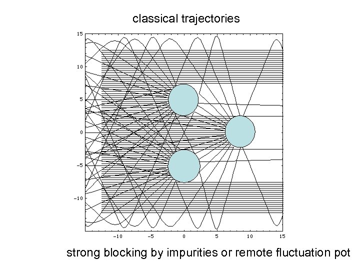
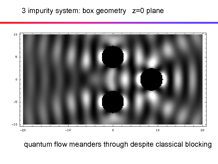
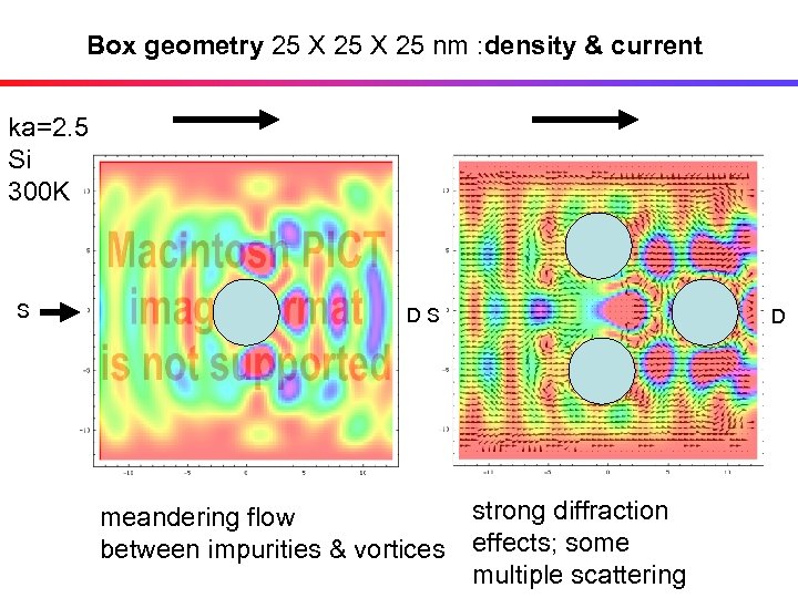
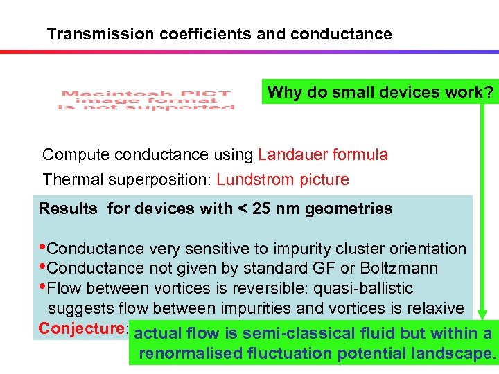
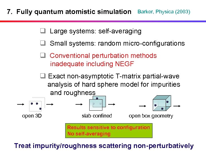 7. Fully quantum atomistic simulation Barker, Physica (2003) q Large systems: self-averaging q Small systems: random micro-configurations q Conventional perturbation methods inadequate including NEGF q Exact non-asymptotic T-matrix partial-wave analysis of hard sphere model for impurities and roughness open 3 D slab confined open box geometry Results sensitive to configuration No self-averaging Treat impurity/roughness scattering non-perturbatively
 Random impurity potential: the Kohn and Luttinger ansatz Fourier transform structure factor ensemble average standard GF theory
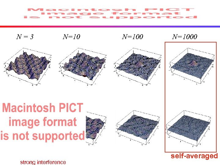 N=3 N=10 strong interference N=1000 self-averaged
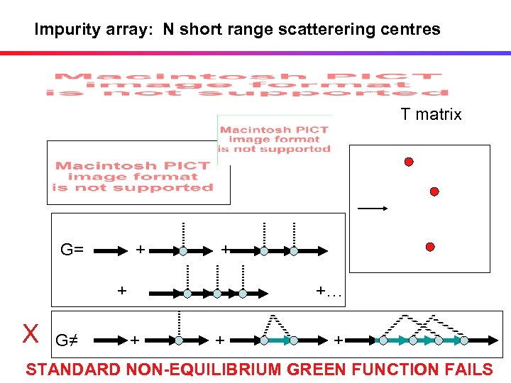 Impurity array: N short range scatterering centres T matrix G= + + + X G≠ +… + + + STANDARD NON-EQUILIBRIUM GREEN FUNCTION FAILS
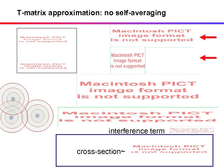 T-matrix approximation: no self-averaging interference term cross-section~
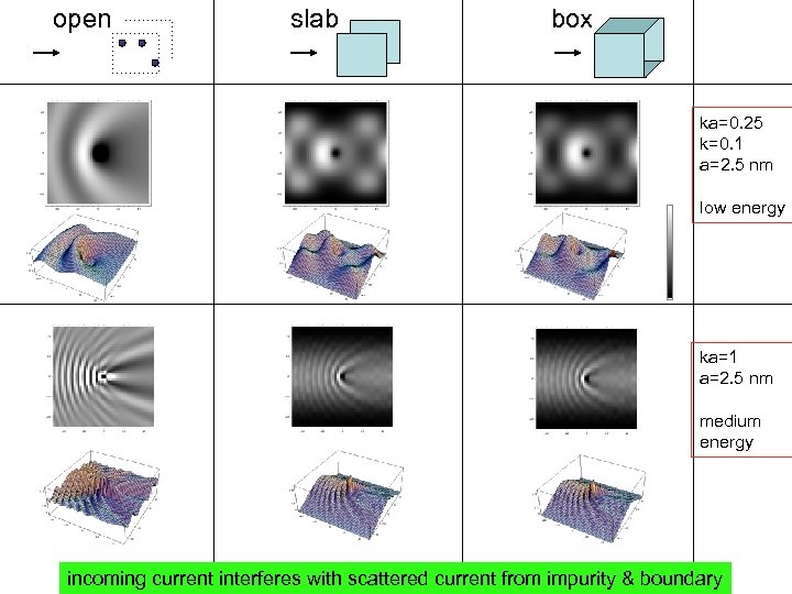 open slab box ka=0. 25 k=0. 1 a=2. 5 nm low energy ka=1 a=2. 5 nm medium energy incoming current interferes with scattered current from impurity & boundary
 classical trajectories strong blocking by impurities or remote fluctuation pot
 3 impurity system: box geometry z=0 plane quantum flow meanders through despite classical blocking
 Box geometry 25 X 25 nm : density & current ka=2. 5 Si 300 K S DS meandering flow between impurities & vortices D strong diffraction effects; some multiple scattering
 Transmission coefficients and conductance Why do small devices work? Compute conductance using Landauer formula Thermal superposition: Lundstrom picture Results for devices with < 25 nm geometries • Conductance very sensitive to impurity cluster orientation • Conductance not given by standard GF or Boltzmann • Flow between vortices is reversible: quasi-ballistic suggests flow between impurities and vortices is relaxive Conjecture: actual flow is semi-classical fluid but within a renormalised fluctuation potential landscape.
 8. Summary • A new interface roughness scattering model developed: gives good agreement with 67 nm n-channel Si and Strained Si MOSFETs. • Design and scaling studies provide useful results for RF and linear devices • A state-of-the-art Monte Carlo simulator • Practical and new ab initio quantum simulation tools • Role of atomicity and fluctuations • Advanced device studies down to 4 nm scale • Silicon nanoelectronics has a great future -lets not ignore it!
 END
END


