35677735e419de4b1bcf7841dab67851.ppt
- Количество слайдов: 24
 Tracking Detector Material Issues for the s. LHC Hartmut F. -W. Sadrozinski SCIPP, UC Santa Cruz, CA 95064 Hartmut F. -W. Sadrozinski, US ATLAS Upgrade Meeting Nov 10, 2005 1
 Outline of the talk - Motivation for R&D in new Detector Materials - Radiation Damage - Initial Results with p-type Detectors - Expected Performance - R&D Plan - Much of the data from RD 50 http: //rd 50. web. cern. ch/rd 50/ - In collaboration with Mara Bruzzi and Abe Seiden - Presumably this is relevant for both strips and pixels - Will not discuss 3 -D detectors here Announcement: 2 nd Trento Workshop on Advanced Detector Design (focus on 3 -D and p-type SSD) Feb 15. – 16. 2006 Hartmut F. -W. Sadrozinski, US ATLAS Upgrade Meeting Nov 10, 2005 2
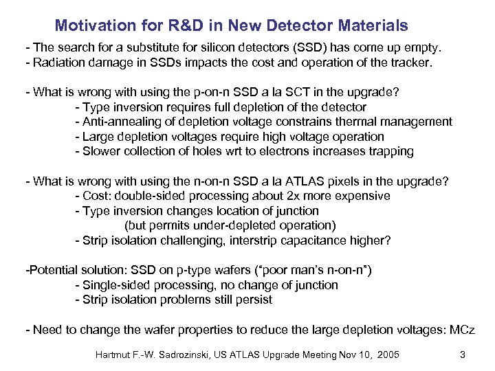 Motivation for R&D in New Detector Materials - The search for a substitute for silicon detectors (SSD) has come up empty. - Radiation damage in SSDs impacts the cost and operation of the tracker. - What is wrong with using the p-on-n SSD a la SCT in the upgrade? - Type inversion requires full depletion of the detector - Anti-annealing of depletion voltage constrains thermal management - Large depletion voltages require high voltage operation - Slower collection of holes wrt to electrons increases trapping - What is wrong with using the n-on-n SSD a la ATLAS pixels in the upgrade? - Cost: double-sided processing about 2 x more expensive - Type inversion changes location of junction (but permits under-depleted operation) - Strip isolation challenging, interstrip capacitance higher? -Potential solution: SSD on p-type wafers (“poor man’s n-on-n”) - Single-sided processing, no change of junction - Strip isolation problems still persist - Need to change the wafer properties to reduce the large depletion voltages: MCz Hartmut F. -W. Sadrozinski, US ATLAS Upgrade Meeting Nov 10, 2005 3
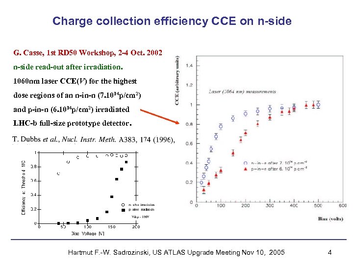 Charge collection efficiency CCE on n-side G. Casse, 1 st RD 50 Workshop, 2 -4 Oct. 2002 n-side read-out after irradiation. 1060 nm laser CCE(V) for the highest dose regions of an n-in-n (7. 1014 p/cm 2) and p-in-n (6. 1014 p/cm 2) irradiated LHC-b full-size prototype detector. Hartmut F. -W. Sadrozinski, US ATLAS Upgrade Meeting Nov 10, 2005 4
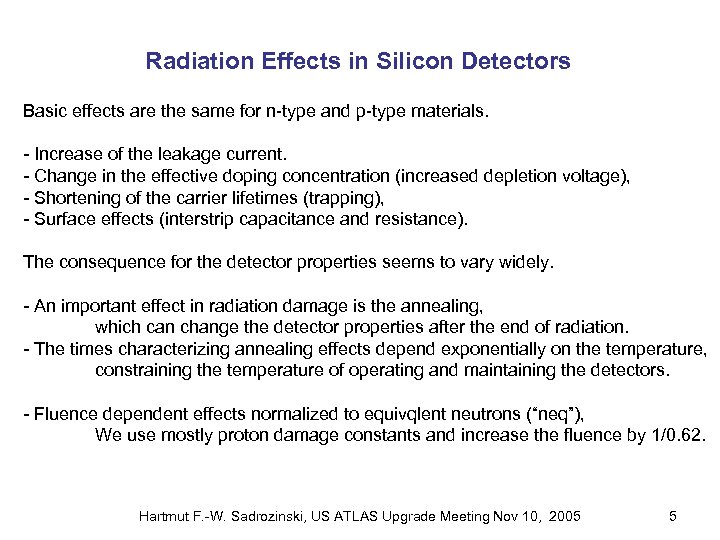 Radiation Effects in Silicon Detectors Basic effects are the same for n-type and p-type materials. - Increase of the leakage current. - Change in the effective doping concentration (increased depletion voltage), - Shortening of the carrier lifetimes (trapping), - Surface effects (interstrip capacitance and resistance). The consequence for the detector properties seems to vary widely. - An important effect in radiation damage is the annealing, which can change the detector properties after the end of radiation. - The times characterizing annealing effects depend exponentially on the temperature, constraining the temperature of operating and maintaining the detectors. - Fluence dependent effects normalized to equivqlent neutrons (“neq”), We use mostly proton damage constants and increase the fluence by 1/0. 62. Hartmut F. -W. Sadrozinski, US ATLAS Upgrade Meeting Nov 10, 2005 5
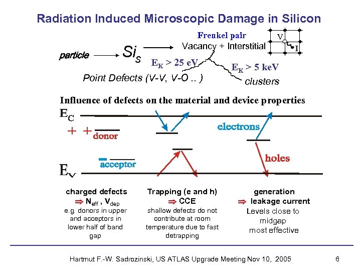 Radiation Induced Microscopic Damage in Silicon particle Sis Frenkel pair Vacancy + Interstitial EK > 25 e. V Point Defects (V-V, V-O. . ) V I EK > 5 ke. V clusters Influence of defects on the material and device properties charged defects Neff , Vdep e. g. donors in upper and acceptors in lower half of band gap Trapping (e and h) CCE shallow defects do not contribute at room temperature due to fast detrapping generation leakage current Levels close to midgap most effective Hartmut F. -W. Sadrozinski, US ATLAS Upgrade Meeting Nov 10, 2005 6
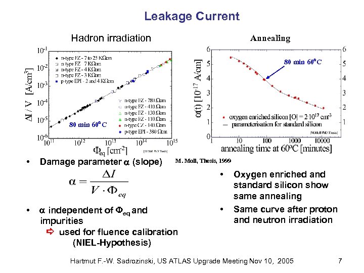 Leakage Current Hadron irradiation Annealing 80 min 60 C • Damage parameter (slope) M. Moll, Thesis, 1999 • • independent of eq and impurities used for fluence calibration (NIEL-Hypothesis) • Oxygen enriched and standard silicon show same annealing Same curve after proton and neutron irradiation Hartmut F. -W. Sadrozinski, US ATLAS Upgrade Meeting Nov 10, 2005 7
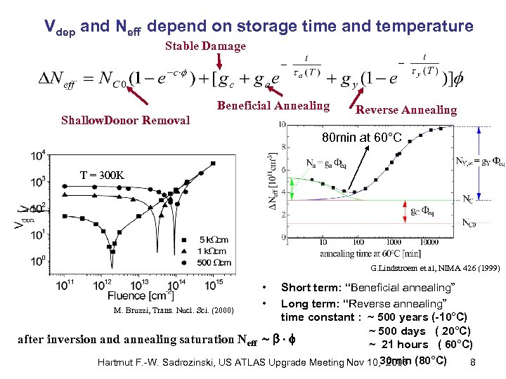 Vdep and Neff depend on storage time and temperature Stable Damage Beneficial Annealing Shallow. Donor Removal Reverse Annealing 80 min at 60°C T = 300 K G. Lindstroem et al, NIMA 426 (1999) • • Short term: “Beneficial annealing” Long term: “Reverse annealing” M. Bruzzi, Trans. Nucl. Sci. (2000) time constant : ~ 500 years (-10°C) ~ 500 days ( 20°C) after inversion and annealing saturation Neff b f ~ 21 hours ( 60°C) Hartmut F. -W. Sadrozinski, US ATLAS Upgrade Meeting Nov 10, 30 min (80°C) 2005 8
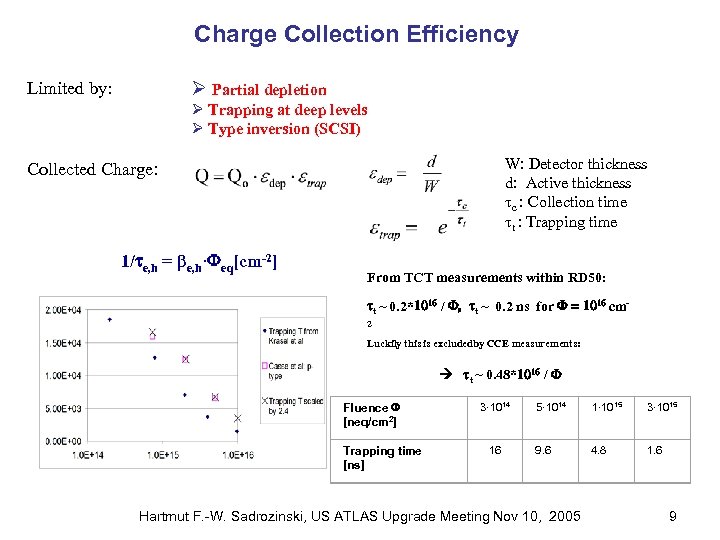 Charge Collection Efficiency Ø Partial depletion Limited by: Ø Trapping at deep levels Ø Type inversion (SCSI) W: Detector thickness d: Active thickness tc : Collection time tt : Trapping time Collected Charge: 1/ e, h = βe, h· eq[cm-2] From TCT measurements within RD 50: t ~ 0. 2*1016 / , t ~ 0. 2 ns for = 1016 cm 2 Luckily this is excludedby CCE measurements: t ~ 0. 48*1016 / Fluence [neq/cm 2] Trapping time [ns] 3· 1014 16 5· 1014 1· 1015 3· 1015 9. 6 4. 8 1. 6 Hartmut F. -W. Sadrozinski, US ATLAS Upgrade Meeting Nov 10, 2005 9
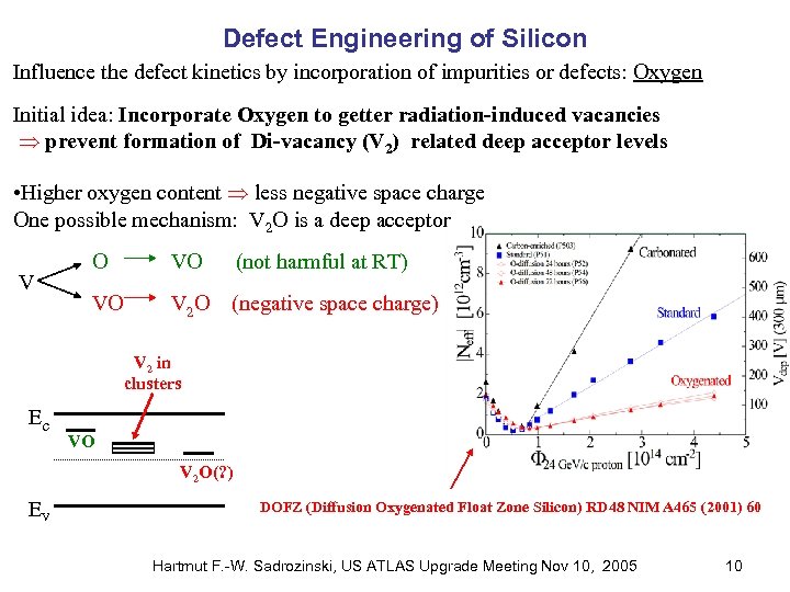 Defect Engineering of Silicon Influence the defect kinetics by incorporation of impurities or defects: Oxygen Initial idea: Incorporate Oxygen to getter radiation-induced vacancies prevent formation of Di-vacancy (V 2) related deep acceptor levels • Higher oxygen content less negative space charge One possible mechanism: V 2 O is a deep acceptor O VO (not harmful at RT) V VO V 2 O (negative space charge) V 2 in clusters Ec VO V 2 O(? ) EV DOFZ (Diffusion Oxygenated Float Zone Silicon) RD 48 NIM A 465 (2001) 60 Hartmut F. -W. Sadrozinski, US ATLAS Upgrade Meeting Nov 10, 2005 10
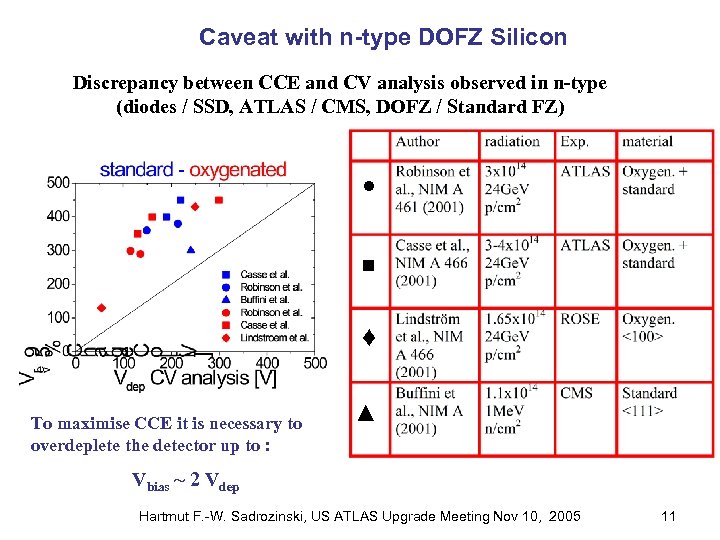 Caveat with n-type DOFZ Silicon Discrepancy between CCE and CV analysis observed in n-type (diodes / SSD, ATLAS / CMS, DOFZ / Standard FZ) ● ■ ♦ To maximise CCE it is necessary to overdeplete the detector up to : ▲ Vbias ~ 2 Vdep Hartmut F. -W. Sadrozinski, US ATLAS Upgrade Meeting Nov 10, 2005 11
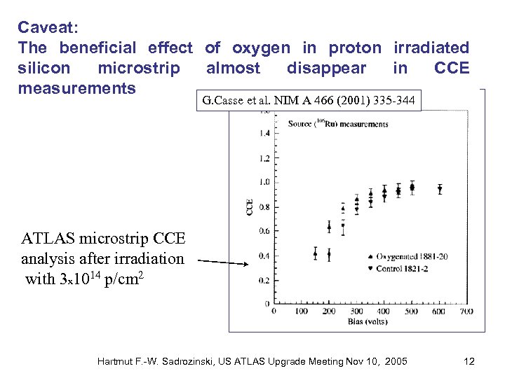 Caveat: The beneficial effect of oxygen in proton irradiated silicon microstrip almost disappear in CCE measurements G. Casse et al. NIM A 466 (2001) 335 -344 ATLAS microstrip CCE analysis after irradiation with 3 x 10¹⁴ p/cm 2 Hartmut F. -W. Sadrozinski, US ATLAS Upgrade Meeting Nov 10, 2005 12
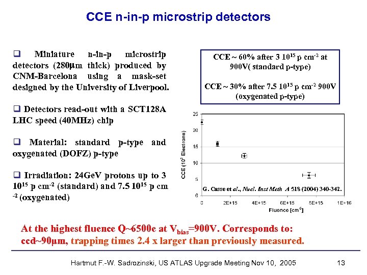 CCE n-in-p microstrip detectors q Miniature n-in-p microstrip detectors (280 mm thick) produced by CNM-Barcelona using a mask-set designed by the University of Liverpool. CCE ~ 60% after 3 1015 p cm-2 at 900 V( standard p-type) CCE ~ 30% after 7. 5 1015 p cm-2 900 V (oxygenated p-type) q Detectors read-out with a SCT 128 A LHC speed (40 MHz) chip q Material: standard p-type and oxygenated (DOFZ) p-type q Irradiation: 24 Ge. V protons up to 3 1015 p cm-2 (standard) and 7. 5 1015 p cm -2 (oxygenated) G. Casse et al. , Nucl. Inst Meth A 518 (2004) 340 -342. At the highest fluence Q~6500 e at Vbias=900 V. Corresponds to: ccd~90µm, trapping times 2. 4 x larger than previously measured. Hartmut F. -W. Sadrozinski, US ATLAS Upgrade Meeting Nov 10, 2005 13
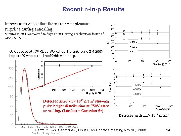 Recent n-in-p Results Important to check that there are no unpleasant surprises during annealing. Minutes at 80 o. C converted to days at 20 o. C using acceleration factor of 7430 (M. Moll). G. Casse et al. , 6 th RD 50 Workshop, Helsinki June 2 -4 2005 http: //rd 50. web. cern. ch/rd 50/6 th-workshop/. Detector after 7. 5× 10¹⁵ p/cm 2 showing pulse height distribution at 750 V after annealing. (Landau + Gaussian fit) Detector with 1. 1× 10¹⁵ p/cm 2 Hartmut F. -W. Sadrozinski, US ATLAS Upgrade Meeting Nov 10, 2005 14
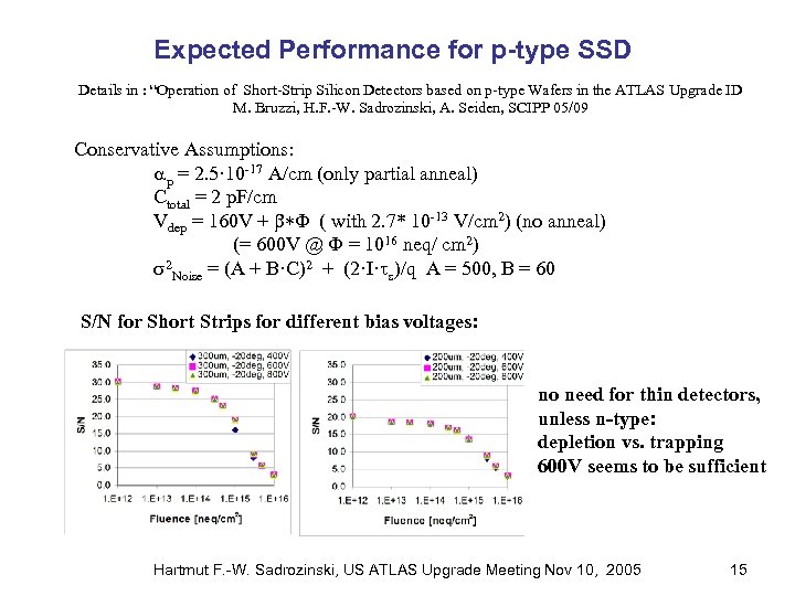 Expected Performance for p-type SSD Details in : “Operation of Short-Strip Silicon Detectors based on p-type Wafers in the ATLAS Upgrade ID M. Bruzzi, H. F. -W. Sadrozinski, A. Seiden, SCIPP 05/09 Conservative Assumptions: ap = 2. 5· 10 -17 A/cm (only partial anneal) Ctotal = 2 p. F/cm Vdep = 160 V + b*F ( with 2. 7* 10 -13 V/cm 2) (no anneal) (= 600 V @ F = 1016 neq/ cm 2) s 2 Noise = (A + B·C)2 + (2·I·ts)/q A = 500, B = 60 S/N for Short Strips for different bias voltages: no need for thin detectors, unless n-type: depletion vs. trapping 600 V seems to be sufficient Hartmut F. -W. Sadrozinski, US ATLAS Upgrade Meeting Nov 10, 2005 15
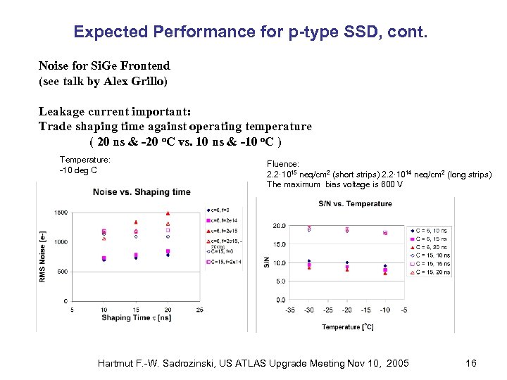 Expected Performance for p-type SSD, cont. Noise for Si. Ge Frontend (see talk by Alex Grillo) Leakage current important: Trade shaping time against operating temperature ( 20 ns & -20 o. C vs. 10 ns & -10 o. C ) Temperature: -10 deg C Fluence: 2. 2· 1015 neq/cm 2 (short strips) 2. 2· 1014 neq/cm 2 (long strips) The maximum bias voltage is 600 V Hartmut F. -W. Sadrozinski, US ATLAS Upgrade Meeting Nov 10, 2005 16
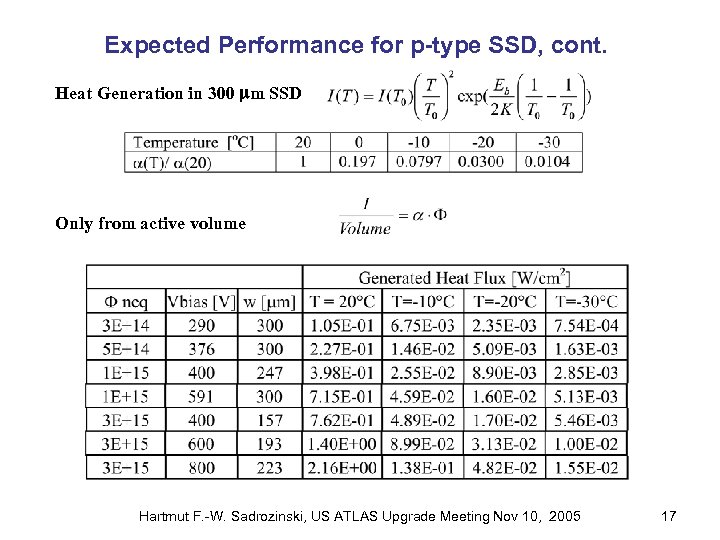 Expected Performance for p-type SSD, cont. Heat Generation in 300 mm SSD Only from active volume Hartmut F. -W. Sadrozinski, US ATLAS Upgrade Meeting Nov 10, 2005 17
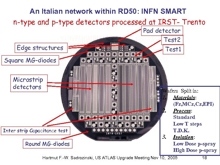 An Italian network within RD 50: INFN SMART n-type and p-type detectors processed at IRST- Trento Edge structures Pad detector Test 2 Test 1 Square MG-diodes Microstrip detectors Inter strip Capacitance test Round MG-diodes Wafers Split in: 1. Materials: (Fz, MCz, EPI) 2. Process: Standard Low T steps T. D. K. 3. Isolation: Low Dose p-spray High Dose p-spray Hartmut F. -W. Sadrozinski, US ATLAS Upgrade Meeting Nov 10, 2005 18
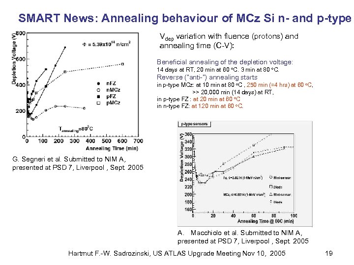 SMART News: Annealing behaviour of MCz Si n- and p-type Vdep variation with fluence (protons) and annealing time (C-V): Beneficial annealing of the depletion voltage: 14 days at RT, 20 min at 60 o. C. 3 min at 80 o. C. Reverse (“anti-”) annealing starts in p-type MCz: at 10 min at 80 o. C , 250 min (=4 hrs) at 60 o. C, >> 20, 000 min (14 days) at RT, in p-type FZ : at 20 min at 60 o. C in n-type FZ: at 120 min at 60 o. C. G. Segneri et al. Submitted to NIM A, presented at PSD 7, Liverpool , Sept. 2005 A. Macchiolo et al. Submitted to NIM A, presented at PSD 7, Liverpool , Sept. 2005 Hartmut F. -W. Sadrozinski, US ATLAS Upgrade Meeting Nov 10, 2005 19
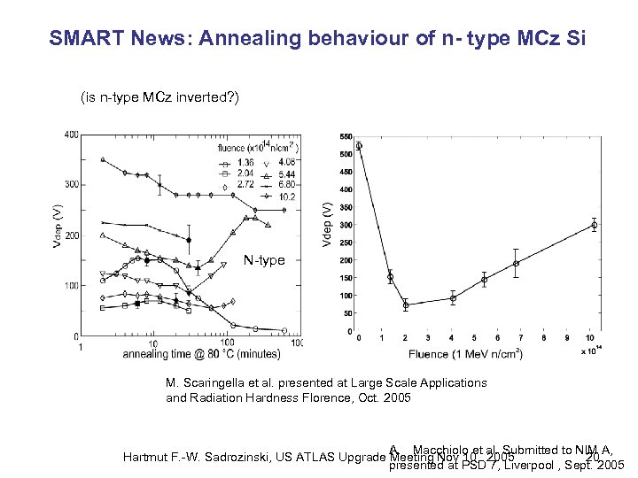 SMART News: Annealing behaviour of n- type MCz Si (is n-type MCz inverted? ) N-type M. Scaringella et al. presented at Large Scale Applications and Radiation Hardness Florence, Oct. 2005 A. Macchiolo et al. Submitted to NIM A, Hartmut F. -W. Sadrozinski, US ATLAS Upgrade Meeting Nov 10, 2005 20 presented at PSD 7, Liverpool , Sept. 2005
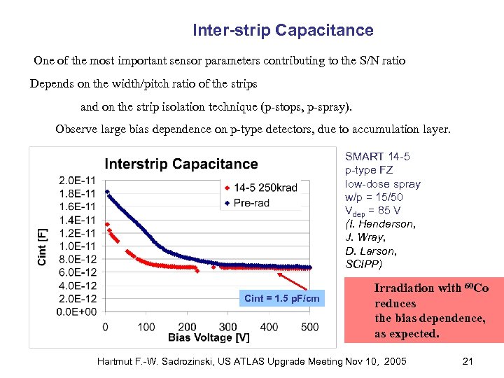 Inter-strip Capacitance One of the most important sensor parameters contributing to the S/N ratio Depends on the width/pitch ratio of the strips and on the strip isolation technique (p-stops, p-spray). Observe large bias dependence on p-type detectors, due to accumulation layer. SMART 14 -5 p-type FZ low-dose spray w/p = 15/50 Vdep = 85 V (I. Henderson, 100 mm pitch J. Wray, D. Larson, SCIPP) Cint = 1. 5 p. F/cm 100 mm pitch Irradiation with 60 Co reduces the bias dependence, as expected. Hartmut F. -W. Sadrozinski, US ATLAS Upgrade Meeting Nov 10, 2005 21
 Status § Radiation hard materials for tracker detectors at Super. LHC are under study by the CERN RD 50 collaboration. Fluence range to be covered with optimised S/N is in the range 1014 -1016 cm-2. At fluences up to 1015 cm-2 (Mid and Outer layers of a SLHC detector) the change of the depletion voltage and the large area to be covered by detectors is the major problem. § High resistivity MCz n-type and p-type Si are most promising materials. § Quite encouragingly, at higher fluences results seem better than first extrapolated from lower fluence: longer trapping times ( p-FZ, p-DOFZ) delayed and reduced reverse annealing ( MCz SMART) sublinear growth of the Vdep with fluence ( p - MCz&FZ) delayed/supressed type inversion ( p- MCZ&FZ, MCz n- protons) § The annealing behavior in both n- and p-type SSD needs to be verified with CCE measurements. Hartmut F. -W. Sadrozinski, US ATLAS Upgrade Meeting Nov 10, 2005 22
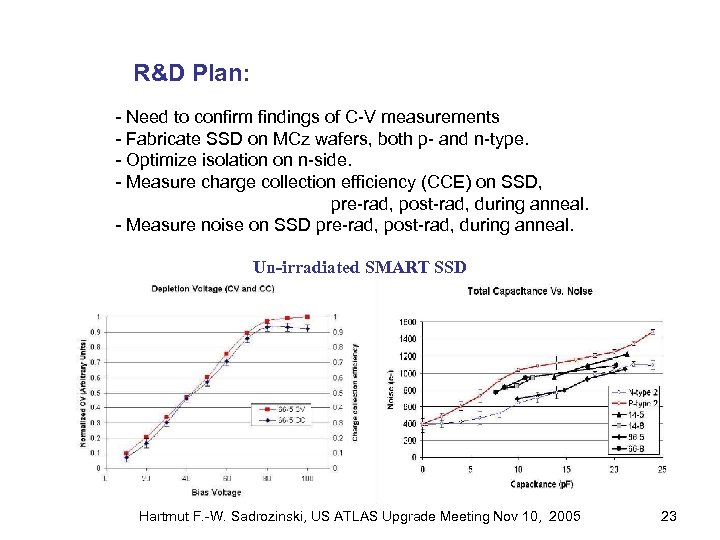 R&D Plan: - Need to confirm findings of C-V measurements - Fabricate SSD on MCz wafers, both p- and n-type. - Optimize isolation on n-side. - Measure charge collection efficiency (CCE) on SSD, pre-rad, post-rad, during anneal. - Measure noise on SSD pre-rad, post-rad, during anneal. Un-irradiated SMART SSD Hartmut F. -W. Sadrozinski, US ATLAS Upgrade Meeting Nov 10, 2005 23
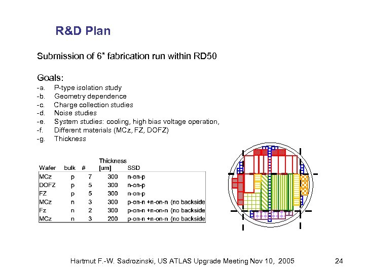 R&D Plan Submission of 6” fabrication run within RD 50 Goals: -a. P-type isolation study -b. Geometry dependence -c. Charge collection studies -d. Noise studies -e. System studies: cooling, high bias voltage operation, -f. Different materials (MCz, FZ, DOFZ) -g. Thickness Hartmut F. -W. Sadrozinski, US ATLAS Upgrade Meeting Nov 10, 2005 24


