148e2ba8028d3287b1d802fd9ae141e1.ppt
- Количество слайдов: 21
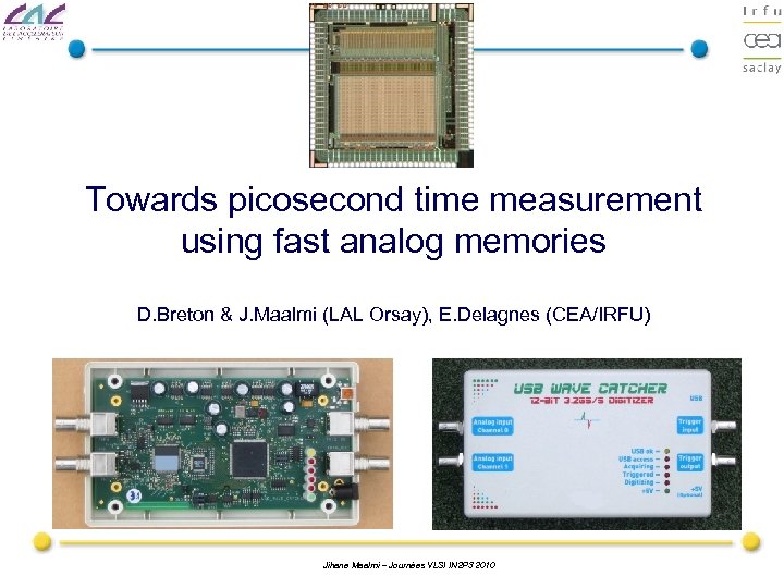 Towards picosecond time measurement using fast analog memories D. Breton & J. Maalmi (LAL Orsay), E. Delagnes (CEA/IRFU) Jihane Maalmi – Journées VLSI IN 2 P 3 2010
 Introduction Why picosecond time measurements? • for Time Of Flight (TOF) detectors in High Energy Physics >> to identify particles (detector goal ~ 25 ps rms) • Medical Imaging : Positron Emission Tomography (PET) >> Time of flight information reduces noise in image • … Goal: measuring the arrival time of fast pulses or time distance between two pulses with a precision better than 10 ps at high scale and low cost For a few channels, just buy a high-end oscilloscope ! Jihane Maalmi – Journées VLSI IN 2 P 3 2010
 State of the art • Existing electronics for time measurement based on Constant Fraction discriminators (CFD) associated with Time to Digital Converters (TDC). • Time resolution of ASICs based on CFDs (no time walk): ~ 30 ps – Pb : one cannot implement a pure delay line in an ASIC. • TDC with voltage ramp: best solution for resolution (~ 10 ps) – Usually used with a Wilkinson ADC for power and simplicity reasons => limited by dead time which can be a problem for high rate experiments • TDC with digital counters and Delay Line Loops (DLL): ~ 25 ps – advantage: produces directly the encoded digital value • Reminder: overall timing resolution is given by the quadratic sum of the discriminator and TDC timing resolutions => > 30 ps • Digital treatment of the digitized signal: – ADCs > 1 GS/s => power, output data rate, need of high-end FPGAs – High Speed Analog Memories: low cost with very low power consumption Jihane Maalmi – Journées VLSI IN 2 P 3 2010
 Why Analog Memories ? • Analog memories look like perfect candidates for high precision time measurements: – – – – They catch the whole signal waveform There is no need for precise discriminators TDC is built-in (position in the memory gives the time) Only the useful information is digitized (vs ADCs) Any type of digital processing can be used Only a few samples/hit are necessary => this limits the dead time Simultaneous write/read operation is feasible, which removes the dead time if necessary • But they have to be carefully designed to reach such a high level of performance … Jihane Maalmi – Journées VLSI IN 2 P 3 2010
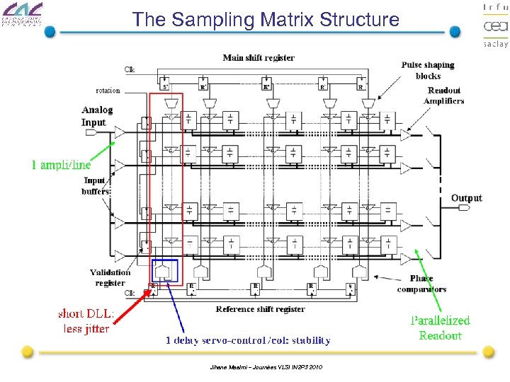 The Sampling Matrix Structure Jihane Maalmi – Journées VLSI IN 2 P 3 2010
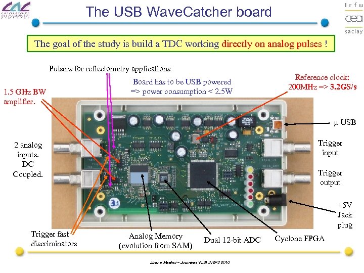 The USB Wave. Catcher board The goal of the study is build a TDC working directly on analog pulses ! Pulsers for reflectometry applications 1. 5 GHz BW amplifier. Board has to be USB powered => power consumption < 2. 5 W Reference clock: 200 MHz => 3. 2 GS/s µ USB Trigger input 2 analog inputs. DC Coupled. Trigger output +5 V Jack plug Trigger fast discriminators Analog Memory (evolution from SAM) Dual 12 -bit ADC Jihane Maalmi – Journées VLSI IN 2 P 3 2010 Cyclone FPGA
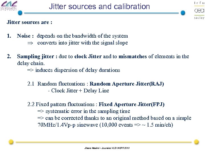 Jitter sources and calibration Jitter sources are : 1. Noise : depends on the bandwidth of the system Þ converts into jitter with the signal slope 2. Sampling jitter : due to clock Jitter and to mismatches of elements in the delay chain. => induces dispersion of delay durations 2. 1 Random fluctuations : Random Aperture Jitter(RAJ) - Clock Jitter + Delay Line 2. 2 Fixed pattern fluctuations : Fixed Aperture Jitter(FPJ) => systematic error in the sampling time => can be corrected thanks to an original method based on a simple 70 MHz/1. 4 Vp-p sinewave (10, 000 events => ~ 1. 5 min/ch) Jihane Maalmi – Journées VLSI IN 2 P 3 2010
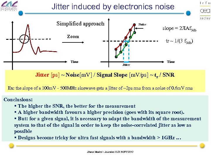 Jitter induced by electronics noise Simplified approach Noise Zoom Time slope = 2 ЛAf 3 db tr ~ 1/(3 f 3 db) Jitter Time Jitter [ps] ~ Noise[m. V] / Signal Slope [m. V/ps] ~ tr / SNR Ex: the slope of a 100 m. V - 500 MHz sinewave gets a jitter of ~2 ps rms from a noise of 0. 6 m. V rms Conclusions: § The higher the SNR, the better for the measurement § A higher bandwidth favours a higher precision (goes with its square root). § But: for a given signal, it is necessary to adapt the bandwidth of the measurement system to that of the signal in order to keep the noise-correlated jitter as low as possible § Designs become tricky for ultra fast signals with a bandwidth > 1 GHz … Jihane Maalmi – Journées VLSI IN 2 P 3 2010
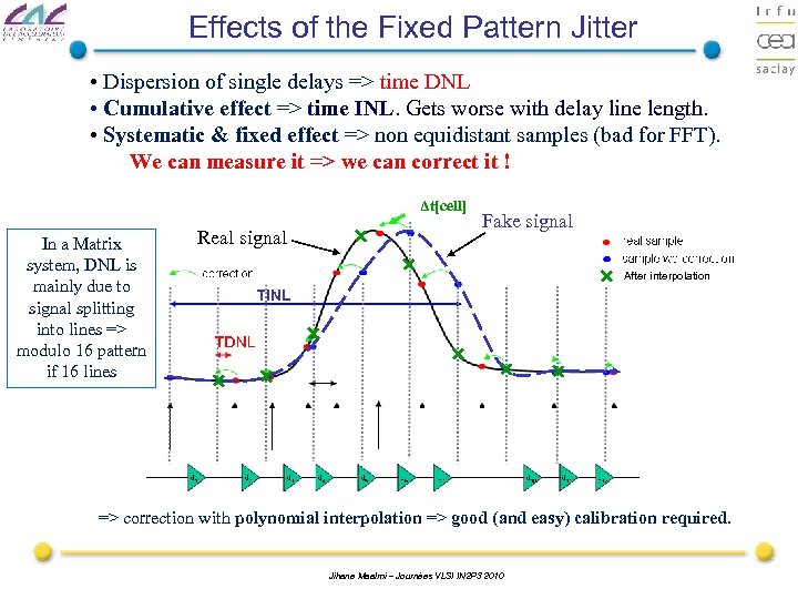 Effects of the Fixed Pattern Jitter • Dispersion of single delays => time DNL • Cumulative effect => time INL. Gets worse with delay line length. • Systematic & fixed effect => non equidistant samples (bad for FFT). We can measure it => we can correct it ! Δt[cell] In a Matrix system, DNL is mainly due to signal splitting into lines => modulo 16 pattern if 16 lines Real signal Fake signal After interpolation => correction with polynomial interpolation => good (and easy) calibration required. Jihane Maalmi – Journées VLSI IN 2 P 3 2010
![Time calibration ØMethod: search of zero-crossing segments of a sine wave => length[position] § Time calibration ØMethod: search of zero-crossing segments of a sine wave => length[position] §](https://present5.com/presentation/148e2ba8028d3287b1d802fd9ae141e1/image-10.jpg) Time calibration ØMethod: search of zero-crossing segments of a sine wave => length[position] § Length[position] is proportional to time step duration assuming that: • sine wave is a straight line (bias ~ 2 ps rms). ØSine wave characteristics: 70 MHz -1. 4 Vpp § Higher frequency => may be bothered by slew rate § Lower frequency => lower slope => more jitter because of noise ØHistogram of Length[position]: § Mean_Length[position]: Fixed Pattern => DNL => INL § Sigma_Length[position]: Random effect => Random Jitter Jihane Maalmi – Journées VLSI IN 2 P 3 2010
Time calibration ØMethod: search of zero-crossing segments of a sine wave => length[position] § Length[position] is proportional to time step duration assuming that: • sine wave is a straight line (bias ~ 2 ps rms). ØSine wave characteristics: 70 MHz -1. 4 Vpp § Higher frequency => may be bothered by slew rate § Lower frequency => lower slope => more jitter because of noise ØHistogram of Length[position]: § Mean_Length[position]: Fixed Pattern => DNL => INL § Sigma_Length[position]: Random effect => Random Jitter Jihane Maalmi – Journées VLSI IN 2 P 3 2010
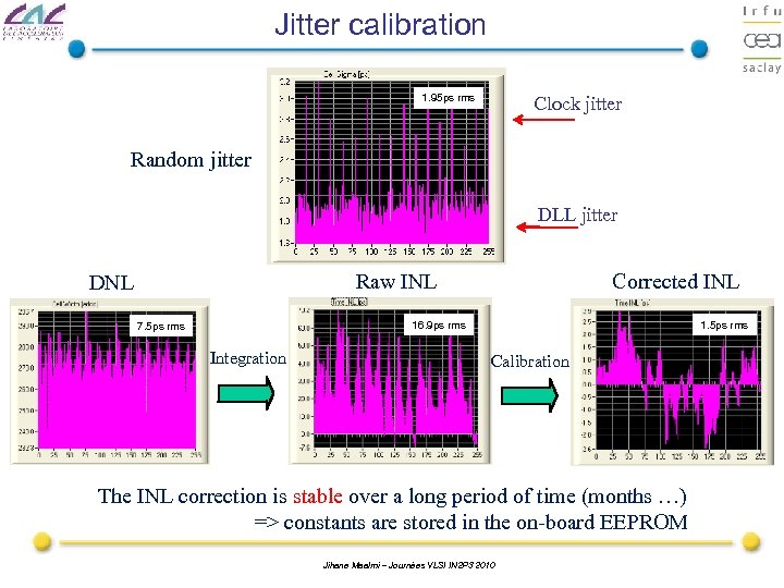 Jitter calibration 1. 95 ps rms Clock jitter Random jitter DLL jitter Corrected INL Raw INL DNL 16. 9 ps rms 7. 5 ps rms Integration 1. 5 ps rms Calibration The INL correction is stable over a long period of time (months …) => constants are stored in the on-board EEPROM Jihane Maalmi – Journées VLSI IN 2 P 3 2010
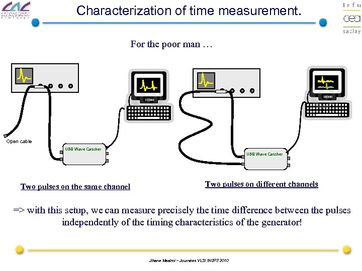 Characterization of time measurement. For the poor man … Open cable USB Wave Catcher Two pulses on the same channel Two pulses on different channels => with this setup, we can measure precisely the time difference between the pulses independently of the timing characteristics of the generator! Jihane Maalmi – Journées VLSI IN 2 P 3 2010
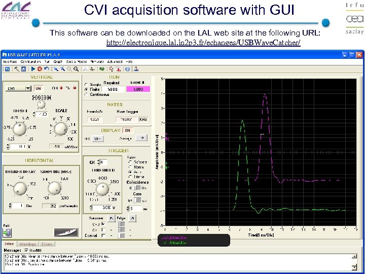 CVI acquisition software with GUI This software can be downloaded on the LAL web site at the following URL: http: //electronique. lal. in 2 p 3. fr/echanges/USBWave. Catcher/ Jihane Maalmi – Journées VLSI IN 2 P 3 2010
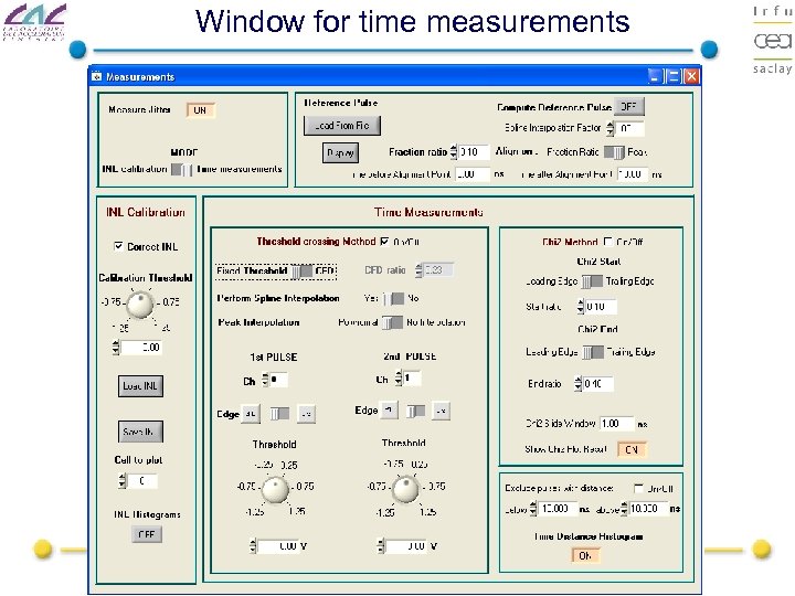 Window for time measurements Jihane Maalmi – Journées VLSI IN 2 P 3 2010
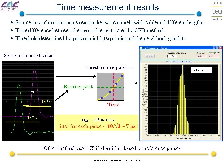 Time measurement results. • Source: asynchronous pulse sent to the two channels with cables of different lengths. • Time difference between the two pulses extracted by CFD method. • Threshold determined by polynomial interpolation of the neighboring points. Spline and normalization Threshold interpolation Ratio to peak 0. 23 Time σΔt ~ 10 ps rms jitter for each pulse ~ 10/√ 2 ~ 7 ps ! Other method used: Chi 2 algorithm based on reference pulses. Jihane Maalmi – Journées VLSI IN 2 P 3 2010 9. 64 ps rms
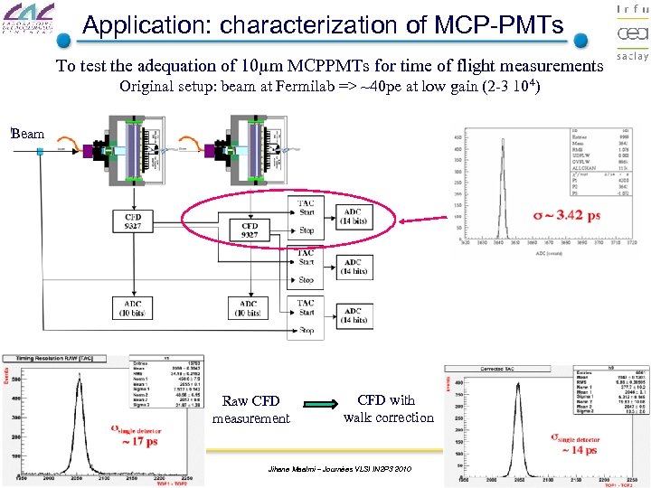 Application: characterization of MCP-PMTs To test the adequation of 10µm MCPPMTs for time of flight measurements Original setup: beam at Fermilab => ~40 pe at low gain (2 -3 104) Beam Raw CFD measurement CFD with walk correction Jihane Maalmi – Journées VLSI IN 2 P 3 2010
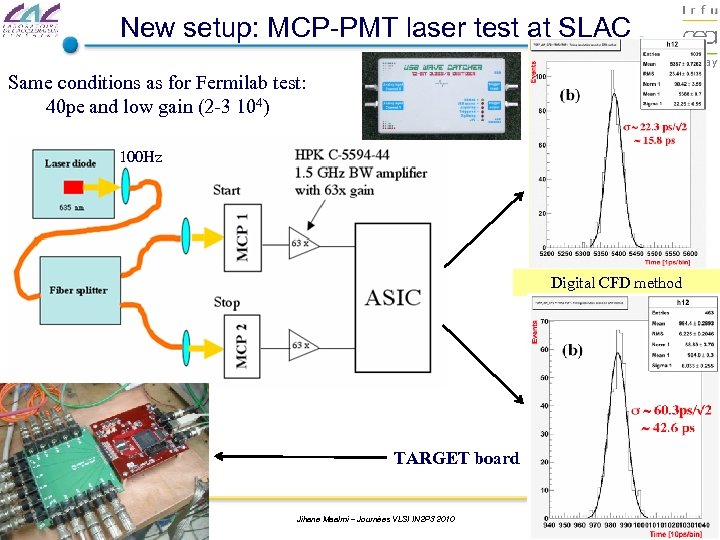 New setup: MCP-PMT laser test at SLAC Same conditions as for Fermilab test: 40 pe and low gain (2 -3 104) 100 Hz Digital CFD method TARGET board Jihane Maalmi – Journées VLSI IN 2 P 3 2010
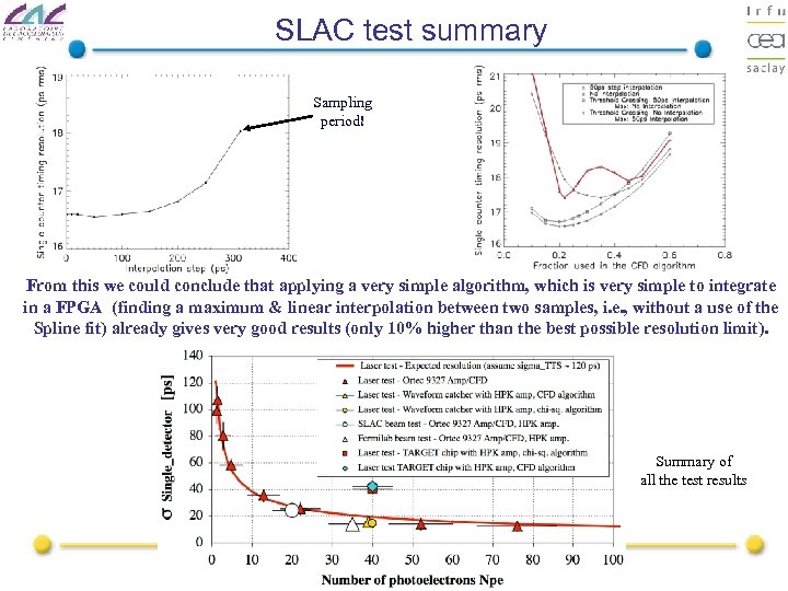 SLAC test summary Sampling period! From this we could conclude that applying a very simple algorithm, which is very simple to integrate in a FPGA (finding a maximum & linear interpolation between two samples, i. e. , without a use of the Spline fit) already gives very good results (only 10% higher than the best possible resolution limit). Summary of all the test results Jihane Maalmi – Journées VLSI IN 2 P 3 2010
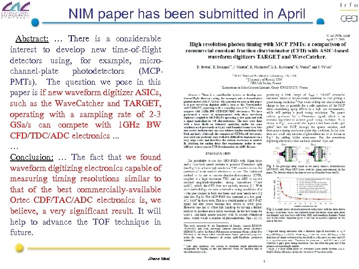 NIM paper has been submitted in April Abstract: … There is a considerable interest to develop new time-of-flight detectors using, for example, microchannel-plate photodetectors (MCPPMTs). The question we pose in this paper is if new waveform digitizer ASICs, such as the Wave. Catcher and TARGET, operating with a sampling rate of 2 -3 GSa/s can compete with 1 GHz BW CFD/TDC/ADC electronics. . . … Conclusion: … The fact that we found waveform digitizing electronics capable of measuring timing resolutions similar to that of the best commercially-available Ortec CDF/TAC/ADC electronics is, we believe, a very significant result. It will help to advance the TOF technique in future. Jihane Maalmi – Journées VLSI IN 2 P 3 2010
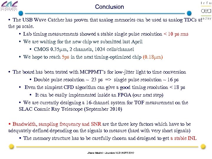 Conclusion • The USB Wave Catcher has proven that analog memories can be used as analog TDCs at the ps scale. • Lab timing measurements showed a stable single pulse resolution < 10 ps rms • We are waiting for the new chip we submitted last April • CMOS 0. 35µm, 2 channels, 1024 cells/channel • We hope to reach 5 ps in the next timing-optimized chip (0. 18µm) • The board has been tested with MCPPMT’s for low-jitter light to time conversion • Double pulse resolution ~ 23 ps => single pulse resolution ~ 16 ps • Even the simplest CFD algorithm can give a good timing resolution < 18 ps • It can be easily implemented inside an FPGA (our next step) • We are currently designing a 16 -channel system for TOF measurement on the SLAC Cosmic Ray Telescope (September 2010) § Bandwidth, sampling frequency and SNR are three key factors which have to be adequately defined depending on the signals to measure (hard with very short signals) § The memory structure has to be carefully chosen and designed to get a stable INL Jihane Maalmi – Journées VLSI IN 2 P 3 2010
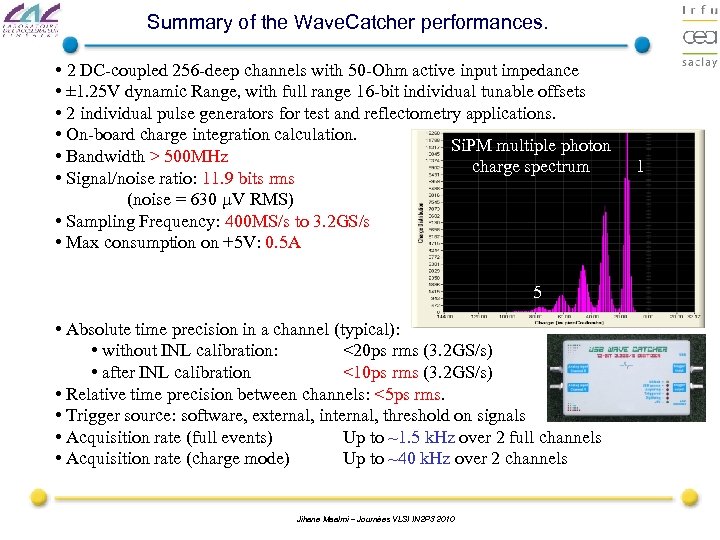 Summary of the Wave. Catcher performances. • 2 DC-coupled 256 -deep channels with 50 -Ohm active input impedance • ± 1. 25 V dynamic Range, with full range 16 -bit individual tunable offsets • 2 individual pulse generators for test and reflectometry applications. • On-board charge integration calculation. Si. PM multiple photon • Bandwidth > 500 MHz charge spectrum • Signal/noise ratio: 11. 9 bits rms (noise = 630 µV RMS) • Sampling Frequency: 400 MS/s to 3. 2 GS/s • Max consumption on +5 V: 0. 5 A 5 • Absolute time precision in a channel (typical): • without INL calibration: <20 ps rms (3. 2 GS/s) • after INL calibration <10 ps rms (3. 2 GS/s) • Relative time precision between channels: <5 ps rms. • Trigger source: software, external, internal, threshold on signals • Acquisition rate (full events) Up to ~1. 5 k. Hz over 2 full channels • Acquisition rate (charge mode) Up to ~40 k. Hz over 2 channels Jihane Maalmi – Journées VLSI IN 2 P 3 2010 1


