ea3c8bba4cbb73f8617e4e910a8466c9.ppt
- Количество слайдов: 65
 TOPS Accurate TOp Level PLL Simulator April 14, 2007 © 2005 -2009 GHz Circuits, Inc. CONFIDENTIAL 1
 Contents • • • Background & Motivation TOPS Overview User Interface Examples Summary Contact info © 2005 -2009 GHz Circuits, Inc. CONFIDENTIAL 2
 Background • • 1. PLLs are complicated 3 rd or higher order, non-linear, discrete -time, time-varying 1 feedback control systems Meeting tight standards mandated goals and even tighter jitter specifications requires extensive expertise, time & compute resources Need answers early in design process for tradeoffs and need exhaustive simulations later on for tolerance/yield analysis There is necessity for a tool which provides circuit-simulator accurate measurements with behavioral-simulator speeds. PLL loop parameters will change with time domain variations in supply (noise) for example, hence these parameters can be considered time-dependent. Also, in some applications like Fractional N synthesizers, the divider counts could be varied in time making the PLL loop parameters time-dependent. © 2005 -2009 GHz Circuits, Inc. CONFIDENTIAL 3
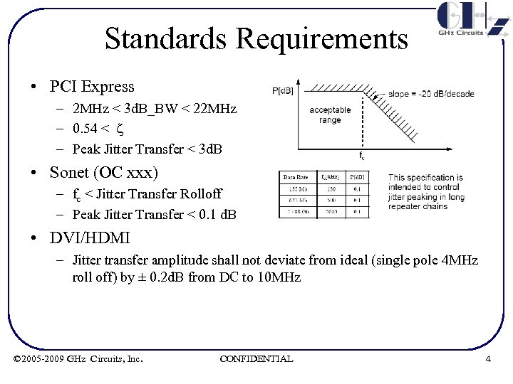 Standards Requirements • PCI Express – 2 MHz < 3 d. B_BW < 22 MHz – 0. 54 < z – Peak Jitter Transfer < 3 d. B • Sonet (OC xxx) – fc < Jitter Transfer Rolloff – Peak Jitter Transfer < 0. 1 d. B • DVI/HDMI – Jitter transfer amplitude shall not deviate from ideal (single pole 4 MHz roll off) by ± 0. 2 d. B from DC to 10 MHz © 2005 -2009 GHz Circuits, Inc. CONFIDENTIAL 4
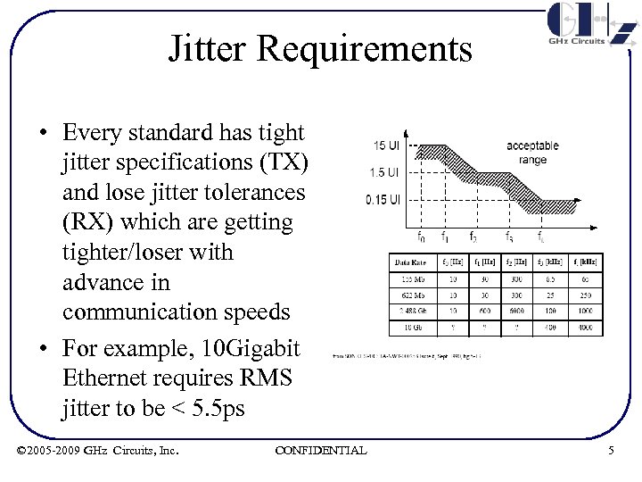 Jitter Requirements • Every standard has tight jitter specifications (TX) and lose jitter tolerances (RX) which are getting tighter/loser with advance in communication speeds • For example, 10 Gigabit Ethernet requires RMS jitter to be < 5. 5 ps © 2005 -2009 GHz Circuits, Inc. CONFIDENTIAL 5
 Design to Standards Compliance Traditional Methods • Rely on “Classical” theory/formulae which erroneously force fits the design to possibly 2 nd order or continuous time domain ? • Rely on in-house developed behavioral code (such as Matlab etc) ? • Run very time consuming transient simulations ? • After running out of time, Rely on “thumb-rules” and “gut-calls” ? • In summary, either “shoot in the dark and hope to hit the target” or expend incredible amounts time and compute resources © 2005 -2009 GHz Circuits, Inc. CONFIDENTIAL 6
 Solution • TOPS: circuit-simulator accurate behavioral simulator with 3 -4 orders of magnitude improvement in speed. • Use TOPS in the architecture phase to determine PLL parameters to meet specifications • Implement circuits per design parameters • Use Circuit Simulator to verify functionality and a few step/impulse response closed loop simulations just to verify TOPS accuracy • Use TOPS with extracted non-linear sub-circuit characteristics for exhaustive tolerance/margin/yield analysis • Use TOPS with time-varying models and noise-scenarios for exhaustive jitter analysis • Get the confidence that circuit will meet specifications pretapeout and simultaneously reap the benefits of time-savings to tapeout. © 2005 -2009 GHz Circuits, Inc. CONFIDENTIAL 7
 TOp level PLL Simulator Overview • A Top Level PLL simulator – ACCURACY: Within a few % accuracy of circuit simulator, with 3 -4 orders of magnitude speed improvement – MODELING: Ability model sub-blocks as linear, nonlinear or time-varying circuit extracts – PARAMETER EXTRACTION: Push button extraction of critical closed loop parameters (ω3 d. B, Jitter Peak, ζ, ωn, Phase-margin) – JITTER ANALYSIS: Comprehensive jitter analysis based on user defined noise vectors © 2005 -2009 GHz Circuits, Inc. CONFIDENTIAL 8
 TOPS User Interface © 2005 -2009 GHz Circuits, Inc. CONFIDENTIAL 9
 TOPS User Interface • Simulator settings tab to select type of analysis • PLL settings tab to specify linear/non-linear PLL parameters such as ICP, KVCO and divider ratios • Filter settings tab to specify linear/non-linear filter parametrs (active/passive, 1/2/3 rd order) • Global Settings tab to select working directory, path to waveform viewers etc. • Active & 3 rd order filters are under development © 2005 -2009 GHz Circuits, Inc. CONFIDENTIAL 10
 Simulator Settings – Single Simulation • User selectable types of analyses – Reference Phase Step (frequency impulse response/phase step response) – Reference Frequency Step (frequency step response) – Reference STFM – User Defined Inputs (for example, Spread Spectrum or Jitter analysis) © 2005 -2009 GHz Circuits, Inc. CONFIDENTIAL 11
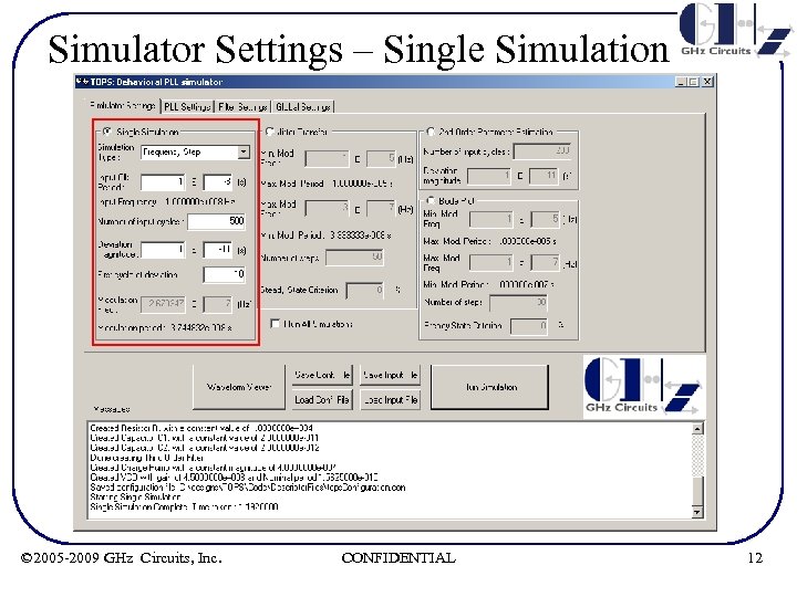 Simulator Settings – Single Simulation © 2005 -2009 GHz Circuits, Inc. CONFIDENTIAL 12
 Simulator Settings – Jitter Transfer • Jitter Transfer (Closed loop BW) measurements – User defines start/stop of modulation frequencies and # of intermediate, logarithmically spaced, frequency points to be analyzed. – User defines steady-state criterion, which is defined as ‘acceptable percentage variation of successive amplitudes of Feedback Clock period deviation’ to determine steadystate condition. Note that even at steady-state, at higher frequencies, successive sinusoidal amplitudes could vary due to the discrete nature of system – TOPS simulates the frequency response in transient domain for each frequency point and outputs ω3 d. B & Jitter Peak © 2005 -2009 GHz Circuits, Inc. CONFIDENTIAL 13
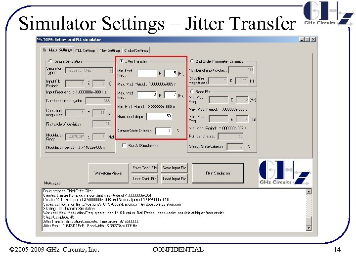 Simulator Settings – Jitter Transfer © 2005 -2009 GHz Circuits, Inc. CONFIDENTIAL 14
 Simulator Settings – Parameter Extraction • 2 nd order Parameter measurements – User defines # of Reference Clock cycles to be simulated – User defines amplitude of Reference frequency step – TOPS simulates the step response, best fits the “classical” 2 nd order response to actual response per two different algorithms and reports, ζ & ωn for each. © 2005 -2009 GHz Circuits, Inc. CONFIDENTIAL 15
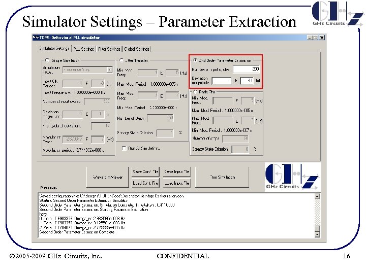 Simulator Settings – Parameter Extraction © 2005 -2009 GHz Circuits, Inc. CONFIDENTIAL 16
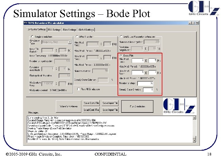
 Simulator Settings – Bode Plot • Bode Plot (Phase Margin measurements) – User defines start/stop of phase modulation frequencies and # of intermediate, logarithmically spaced, frequency points in between – User defines steady-state criterion, which is defined as ‘acceptable percentage variation of successive amplitudes of output phase deviation’ to determine steady-state condition. Note that even at steady-state, at higher frequencies, successive sinusoidal amplitudes could vary due to the discrete nature of system – TOPS simulates the open loop frequency response in transient domain for each frequency point and outputs the Bode Plot & Phase Margin © 2005 -2009 GHz Circuits, Inc. CONFIDENTIAL 17
 Simulator Settings – Bode Plot © 2005 -2009 GHz Circuits, Inc. CONFIDENTIAL 18
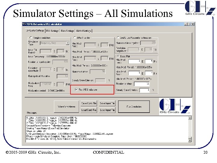
 Simulator Settings – All Simulations • Check this button and click Run to report results for all the below analyses – Jitter transfer (w 3 db & Jitter Peak) – 2 nd order Parameter Estimation (z & wn) – Bode Plot (Phase Margin) © 2005 -2009 GHz Circuits, Inc. CONFIDENTIAL 19
 Simulator Settings – All Simulations © 2005 -2009 GHz Circuits, Inc. CONFIDENTIAL 20
 PLL Settings • KVCO and ICP can either be set linear, non-linear or time-varying. Non-linear or time-varying characteristics should be specified in an ASCII file and appropriately loaded. • Dividers can either be time-invariant or time-varying (ex: for Fractional-N synthesizers) • TPVCO(Nom) is the frequency of the VCO at nominal control voltage. This allows the PLL to either be started from lock, or be allowed to acquire lock. © 2005 -2009 GHz Circuits, Inc. CONFIDENTIAL 21
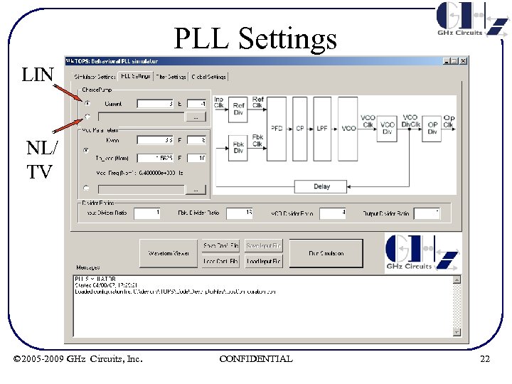 PLL Settings LIN NL/ TV © 2005 -2009 GHz Circuits, Inc. CONFIDENTIAL 22
 Filter Settings • Filter parameters can either be set linear or non -linear. Non-linear characteristics should be specified in an ASCII file and appropriately loaded. • 3 rd order Filter and capacitor leakage models are not yet implemented in this release © 2005 -2009 GHz Circuits, Inc. CONFIDENTIAL 23
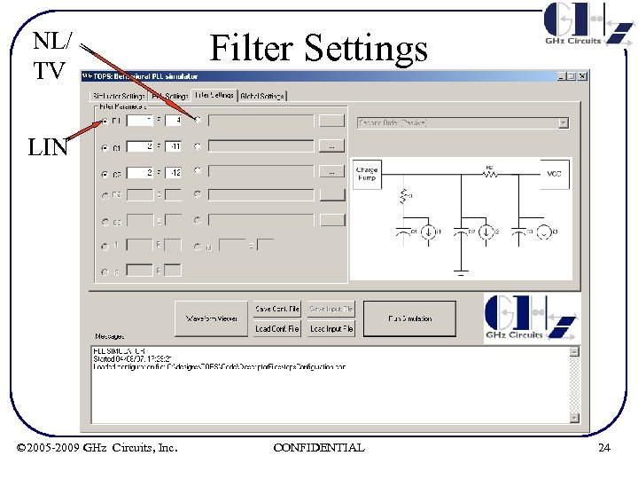 NL/ TV Filter Settings LIN © 2005 -2009 GHz Circuits, Inc. CONFIDENTIAL 24
 Global Settings • Working directory can be specified by user. This is where the configuration file and simulation outputs are placed • User can specify his/her choice of waveform viewer. Currently the results are output in the following formats – – Synopsys Awaves Cadence BDA Plain Text © 2005 -2009 GHz Circuits, Inc. CONFIDENTIAL 25
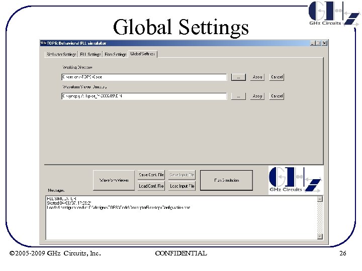 Global Settings © 2005 -2009 GHz Circuits, Inc. CONFIDENTIAL 26
 Examples © 2005 -2009 GHz Circuits, Inc. CONFIDENTIAL 27
 Application Examples 1. 10 Gb. E: PLL Phase step response and verification of accuracy against Cadence Spectre results 2. SATA: PLL acquisition characteristics 3. SATA: PLL spread spectrum response 4. PCI-Express: Jitter Transfer characteristics 5. PCI-Express: 2 nd Order parameter (ζ & ωn) estimation 6. 10 Gb. E: Bode-Plot & Phase Margin measurement © 2005 -2009 GHz Circuits, Inc. CONFIDENTIAL 28
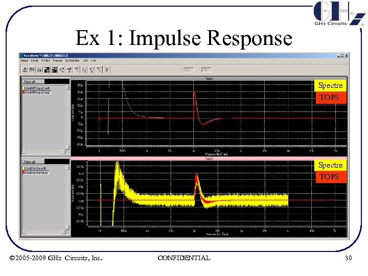
 Ex 1: Single Simulation – Impulse Response • Impulse response for a fully differential 6. 4 GHz LC oscillator is simulated in Circuit Simulator (Cadence Spectre) & TOPS • PLL is allowed to lock in Circuit simulator and a Reference Clock phase step of 200 ps is applied at 2 u. S • PLL is modeled as a linear system in TOPS with circuit extracted parameters. See Ex 6 for parameter listing • Next page shows superposition of the phase tracking error & instantaneous VCO frequency for both Circuit Simulator & TOPS • Output is viewed with Synopsys AWAVES waveform viewer © 2005 -2009 GHz Circuits, Inc. CONFIDENTIAL 29
 Ex 1: Impulse Response Spectre TOPS © 2005 -2009 GHz Circuits, Inc. CONFIDENTIAL 30
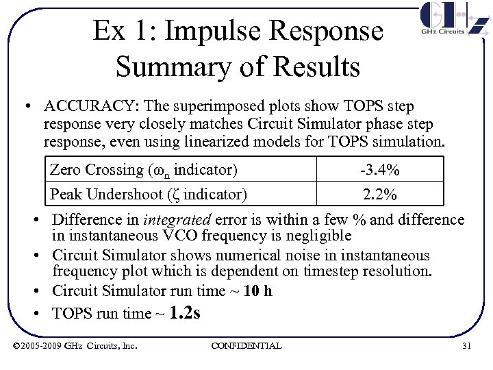 Ex 1: Impulse Response Summary of Results • ACCURACY: The superimposed plots show TOPS step response very closely matches Circuit Simulator phase step response, even using linearized models for TOPS simulation. Zero Crossing (ωn indicator) Peak Undershoot (ζ indicator) -3. 4% 2. 2% • Difference in integrated error is within a few % and difference in instantaneous VCO frequency is negligible • Circuit Simulator shows numerical noise in instantaneous frequency plot which is dependent on timestep resolution. • Circuit Simulator run time ~ 10 h • TOPS run time ~ 1. 2 s © 2005 -2009 GHz Circuits, Inc. CONFIDENTIAL 31
 Ex 2: Single Simulation - Acquisition • The acquisition behavior of a SATA PLL is simulated. See Ex 3 for PLL parameter listing • The next page shows acquisition plots of PFD input tracking error and instantaneous VCO frequency • The model is accurate for small and large signal • Simulation for 10 us takes < 1 s © 2005 -2009 GHz Circuits, Inc. CONFIDENTIAL 32
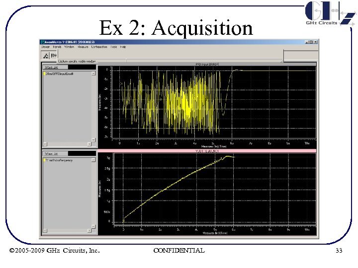 Ex 2: Acquisition © 2005 -2009 GHz Circuits, Inc. CONFIDENTIAL 33
 Ex 3: Single Simulation – UDI (User Defined Input) • The spread spectrum response of a SATA PLL is analyzed • The filter capacitor is varied to observe variations in tracking error © 2005 -2009 GHz Circuits, Inc. CONFIDENTIAL 34
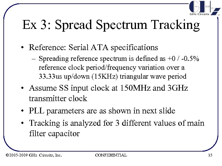 Ex 3: Spread Spectrum Tracking • Reference: Serial ATA specifications – Spreading reference spectrum is defined as +0 / -0. 5% reference clock period/frequency variation over a 33. 33 us up/down (15 KHz) triangular wave period • Assume SS input clock at 150 MHz and 3 GHz transmitter clock • PLL parameters are as shown in next slide • Tracking is analyzed for 3 different values of main filter capacitor © 2005 -2009 GHz Circuits, Inc. CONFIDENTIAL 35
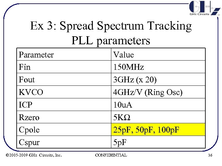 Ex 3: Spread Spectrum Tracking PLL parameters Parameter Fin Fout KVCO ICP Rzero Cpole Cspur © 2005 -2009 GHz Circuits, Inc. Value 150 MHz 3 GHz (x 20) 4 GHz/V (Ring Osc) 10 u. A 5 KΩ 25 p. F, 50 p. F, 100 p. F 5 p. F CONFIDENTIAL 36
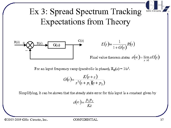 Ex 3: Spread Spectrum Tracking Expectations from Theory R(s) + E(s) _ C(s) G(s) Final value theorem states For an input frequency ramp (parabolic in phase), Rfr(s) = 1/s 3. Simplifying, it can be shown that the steady state error for this input is a constant given by © 2005 -2009 GHz Circuits, Inc. CONFIDENTIAL 37
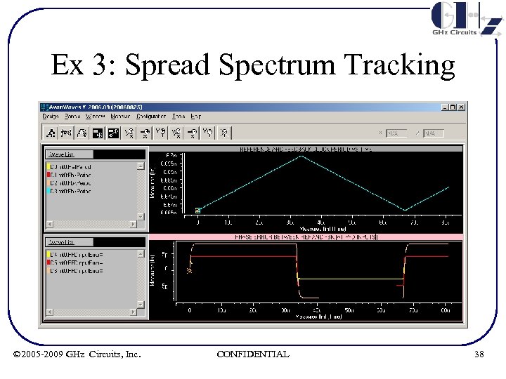 Ex 3: Spread Spectrum Tracking © 2005 -2009 GHz Circuits, Inc. CONFIDENTIAL 38
 Ex 3: Spread Spectrum Tracking Summary & Run time statistics • As expected from theory, tracking error increases with P 1 (i. e. as Cpole increases, tracking error increases) • Each simulation run was for ~ 80 us – About 12 K 150 MHz cycles – About 240 K 3 GHz VCO cycles – Simulation time < 5 s © 2005 -2009 GHz Circuits, Inc. CONFIDENTIAL 39
 Ex 4: Jitter Transfer • The Jitter Transfer (closed loop BW) of a PCIExpress PLL is analyzed • The parameters for the PLL is shown in the next slide • The zero-resistor is varied to see effect on the Jitter Peaking © 2005 -2009 GHz Circuits, Inc. CONFIDENTIAL 40
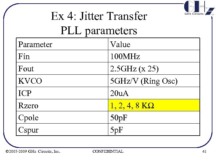 Ex 4: Jitter Transfer PLL parameters Parameter Fin Fout KVCO ICP Rzero Cpole Cspur © 2005 -2009 GHz Circuits, Inc. Value 100 MHz 2. 5 GHz (x 25) 5 GHz/V (Ring Osc) 20 u. A 1, 2, 4, 8 KΩ 50 p. F 5 p. F CONFIDENTIAL 41
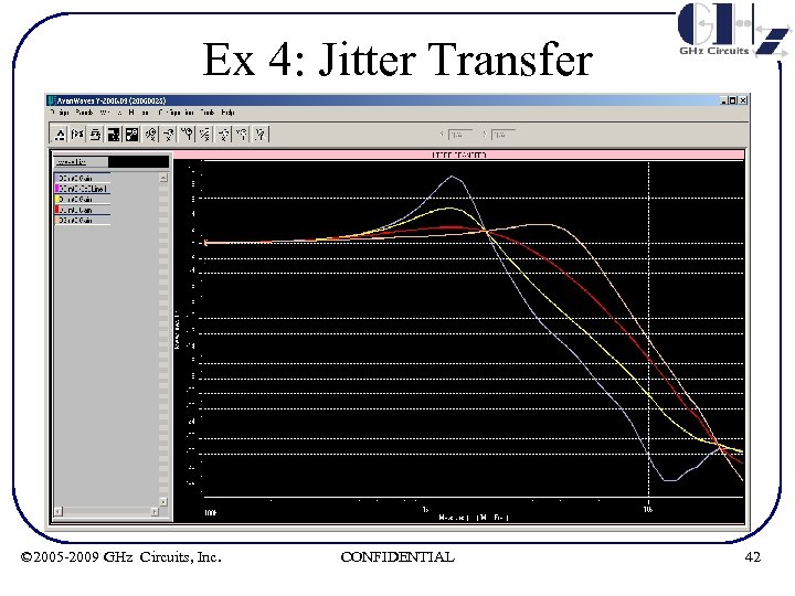 Ex 4: Jitter Transfer © 2005 -2009 GHz Circuits, Inc. CONFIDENTIAL 42
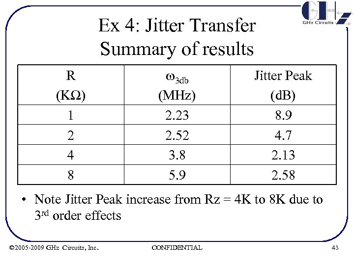 Ex 4: Jitter Transfer Summary of results R (KΩ) 1 2 4 8 w 3 db (MHz) 2. 23 2. 52 3. 8 5. 9 Jitter Peak (d. B) 8. 9 4. 7 2. 13 2. 58 • Note Jitter Peak increase from Rz = 4 K to 8 K due to 3 rd order effects © 2005 -2009 GHz Circuits, Inc. CONFIDENTIAL 43
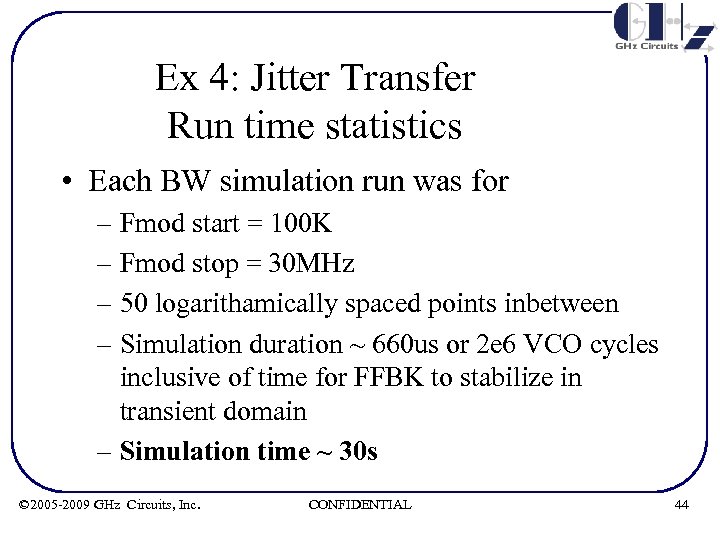 Ex 4: Jitter Transfer Run time statistics • Each BW simulation run was for – Fmod start = 100 K – Fmod stop = 30 MHz – 50 logarithamically spaced points inbetween – Simulation duration ~ 660 us or 2 e 6 VCO cycles inclusive of time for FFBK to stabilize in transient domain – Simulation time ~ 30 s © 2005 -2009 GHz Circuits, Inc. CONFIDENTIAL 44
 Ex 5: 2 nd order Parameter Estimation • The 2 nd order parameters (ζ & ωn) of the previous PCI -Express PLL is analyzed • The analysis is for the same variation of zero-resistor as mentioned previously • The next 4 graphs show the actual response of the PLL to a freq step vs. the best fit per 2 algorithms – Notice the 3 rd order effects manifesting in the step response as Rspur increases. • Which of the 2 algorithms better fits the PLL response is dependent on many factors and it is left to the user to select best fit © 2005 -2009 GHz Circuits, Inc. CONFIDENTIAL 45
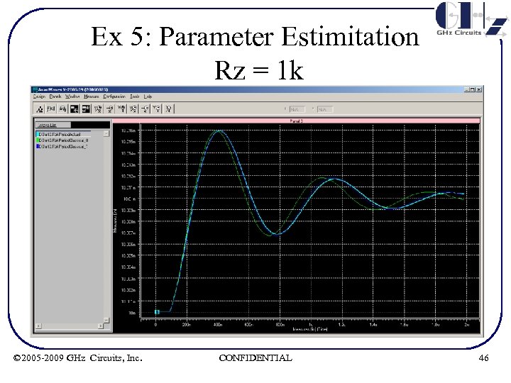 Ex 5: Parameter Estimitation Rz = 1 k © 2005 -2009 GHz Circuits, Inc. CONFIDENTIAL 46
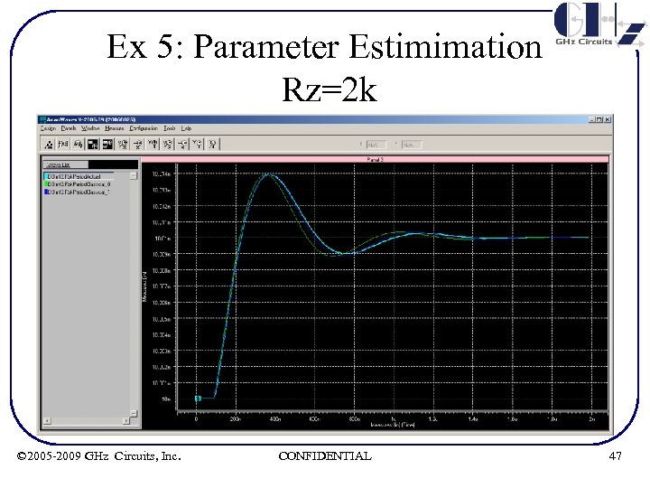 Ex 5: Parameter Estimimation Rz=2 k © 2005 -2009 GHz Circuits, Inc. CONFIDENTIAL 47
 Ex 5: Parameter Estimation Rz=4 k © 2005 -2009 GHz Circuits, Inc. CONFIDENTIAL 48
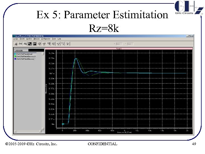 Ex 5: Parameter Estimitation Rz=8 k © 2005 -2009 GHz Circuits, Inc. CONFIDENTIAL 49
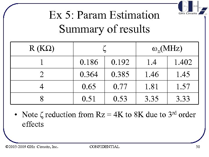 Ex 5: Param Estimation Summary of results R (KΩ) ζ ωn(MHz) 1 2 0. 186 0. 364 0. 192 0. 385 1. 46 1. 402 1. 45 4 8 0. 65 0. 51 0. 77 0. 53 1. 81 3. 35 1. 57 3. 33 • Note ζ reduction from Rz = 4 K to 8 K due to 3 rd order effects © 2005 -2009 GHz Circuits, Inc. CONFIDENTIAL 50
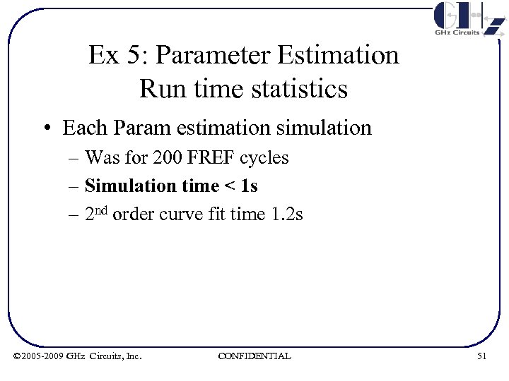 Ex 5: Parameter Estimation Run time statistics • Each Param estimation simulation – Was for 200 FREF cycles – Simulation time < 1 s – 2 nd order curve fit time 1. 2 s © 2005 -2009 GHz Circuits, Inc. CONFIDENTIAL 51
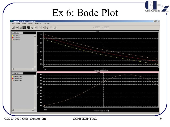
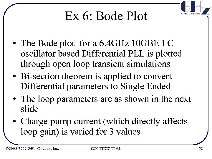 Ex 6: Bode Plot • The Bode plot for a 6. 4 GHz 10 GBE LC oscillator based Differential PLL is plotted through open loop transient simulations • Bi-section theorem is applied to convert Differential parameters to Single Ended • The loop parameters are as shown in the next slide • Charge pump current (which directly affects loop gain) is varied for 3 values © 2005 -2009 GHz Circuits, Inc. CONFIDENTIAL 52
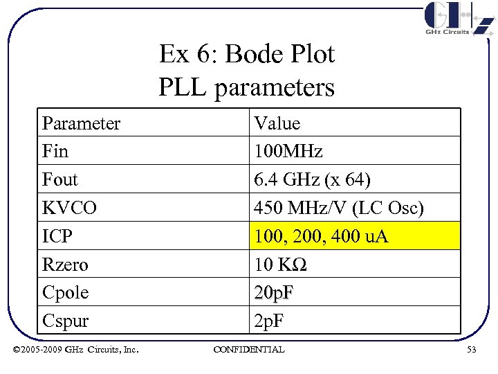 Ex 6: Bode Plot PLL parameters Parameter Fin Fout KVCO ICP Rzero Cpole Cspur © 2005 -2009 GHz Circuits, Inc. Value 100 MHz 6. 4 GHz (x 64) 450 MHz/V (LC Osc) 100, 200, 400 u. A 10 KΩ 20 p. F 2 p. F CONFIDENTIAL 53
 Ex 6: Bode Plot © 2005 -2009 GHz Circuits, Inc. CONFIDENTIAL 54
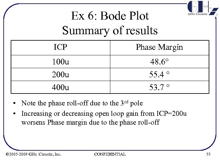 Ex 6: Bode Plot Summary of results ICP Phase Margin 100 u 200 u 48. 6° 55. 4 ° 400 u 53. 7 ° • Note the phase roll-off due to the 3 rd pole • Increasing or decreasing open loop gain from ICP=200 u worsens Phase margin due to the phase roll-off © 2005 -2009 GHz Circuits, Inc. CONFIDENTIAL 55
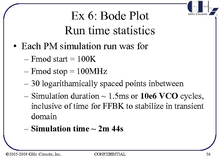 Ex 6: Bode Plot Run time statistics • Each PM simulation run was for – Fmod start = 100 K – Fmod stop = 100 MHz – 30 logarithamically spaced points inbetween – Simulation duration ~ 1. 5 ms or 10 e 6 VCO cycles, inclusive of time for FFBK to stabilize in transient domain – Simulation time ~ 2 m 44 s © 2005 -2009 GHz Circuits, Inc. CONFIDENTIAL 56
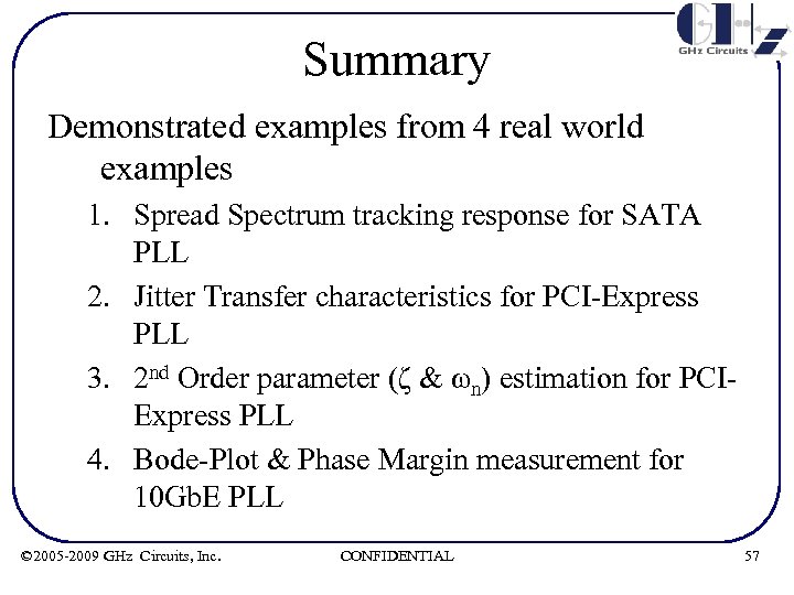 Summary Demonstrated examples from 4 real world examples 1. Spread Spectrum tracking response for SATA PLL 2. Jitter Transfer characteristics for PCI-Express PLL 3. 2 nd Order parameter (ζ & ωn) estimation for PCIExpress PLL 4. Bode-Plot & Phase Margin measurement for 10 Gb. E PLL © 2005 -2009 GHz Circuits, Inc. CONFIDENTIAL 57
 Contact Info Nandu Bhagwan GHz Circuits, Inc 1030 E. El Camino Real, PMB 232 Sunnyvale, CA 94087 (408)7/8/1�/9/8/9/ www. ghzcircuits. com Nandu_at_ghzcircuits_dot_com © 2005 -2009 GHz Circuits, Inc. CONFIDENTIAL 58
 Backups © 2005 -2009 GHz Circuits, Inc. CONFIDENTIAL 59
 Planned Enhancements • Add 3 rd order Filters (with leakage models) and active Filter library • Add hooks to apply user defined jitter at different points (VCO, delay path etc) • Add jitter generation & visualization tools • Add optimization core • Add formal-verification core © 2005 -2009 GHz Circuits, Inc. CONFIDENTIAL 60
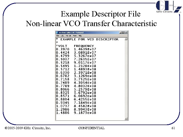 Example Descriptor File Non-linear VCO Transfer Characteristic © 2005 -2009 GHz Circuits, Inc. CONFIDENTIAL 61
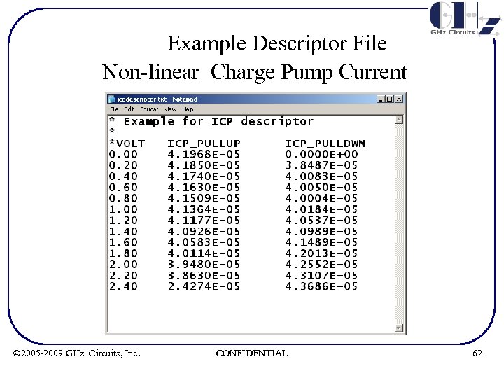 Example Descriptor File Non-linear Charge Pump Current © 2005 -2009 GHz Circuits, Inc. CONFIDENTIAL 62
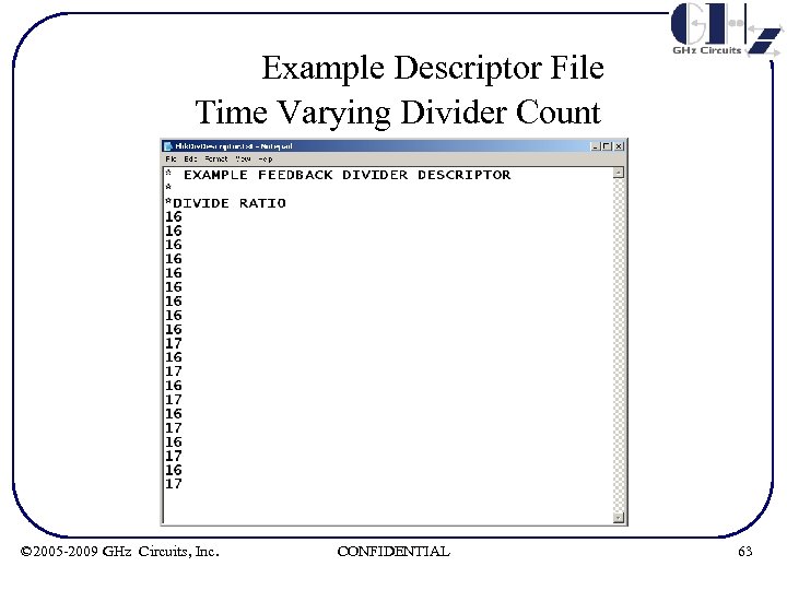 Example Descriptor File Time Varying Divider Count © 2005 -2009 GHz Circuits, Inc. CONFIDENTIAL 63
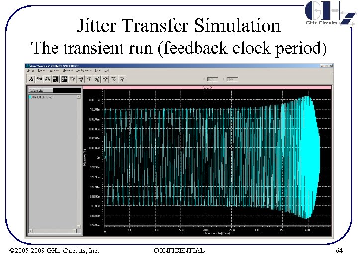 Jitter Transfer Simulation The transient run (feedback clock period) © 2005 -2009 GHz Circuits, Inc. CONFIDENTIAL 64
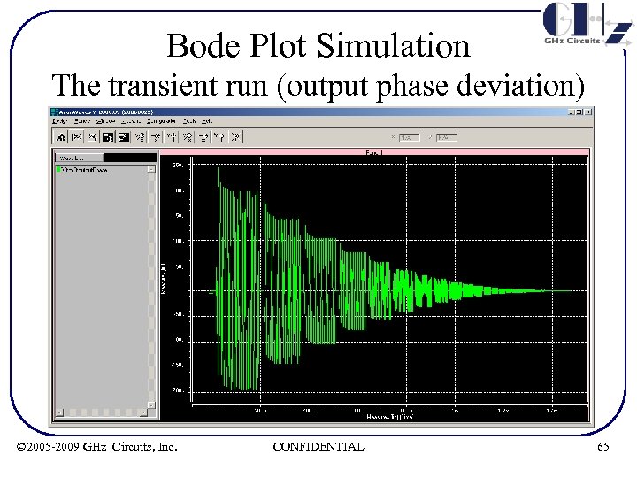 Bode Plot Simulation The transient run (output phase deviation) © 2005 -2009 GHz Circuits, Inc. CONFIDENTIAL 65


