
The World Leader in High-Performance Signal Processing Solutions


dds_analog_devices.ppt
- Размер: 2.1 Mегабайта
- Количество слайдов: 50
Описание презентации The World Leader in High-Performance Signal Processing Solutions по слайдам
The World Leader in High-Performance Signal Processing Solutions 1. Theory (why & how it works) 2. Error Sources 3. Advanced DDS Capabilities 4. Applications Examples Direct Digital Synthesis Theory & Applications paul. smith@analog. com
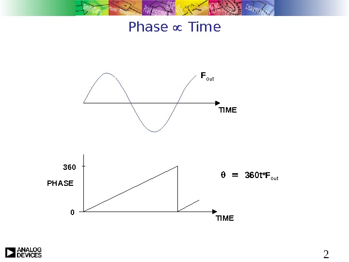
2 Phase Time 360 t*F out. TIMEF out TIME 0 PHAS
3 Discrete Phase Discrete Time PHASE TIME 2 n -1 0 n clk out 2 F F F out clk.
4 How do you build this? PHASE TIME 2 n -1 0 n clk out 2 F F n. PHASE REGISTER CLOCKn. PHASE ACCUMULATOR n 1 n = 24 — 48 BITS F clk
5 Changing Frequency PHASE TIME 2 n -1 0 n clk out 2 F MF n. PHASE REGISTER CLOCKn. PHASE ACCUMULATOR nn = 24 — 48 BITS M FREQUENCY CONTROL M = TUNING WORD DELTA PHASE REGISTER Mn M F clk
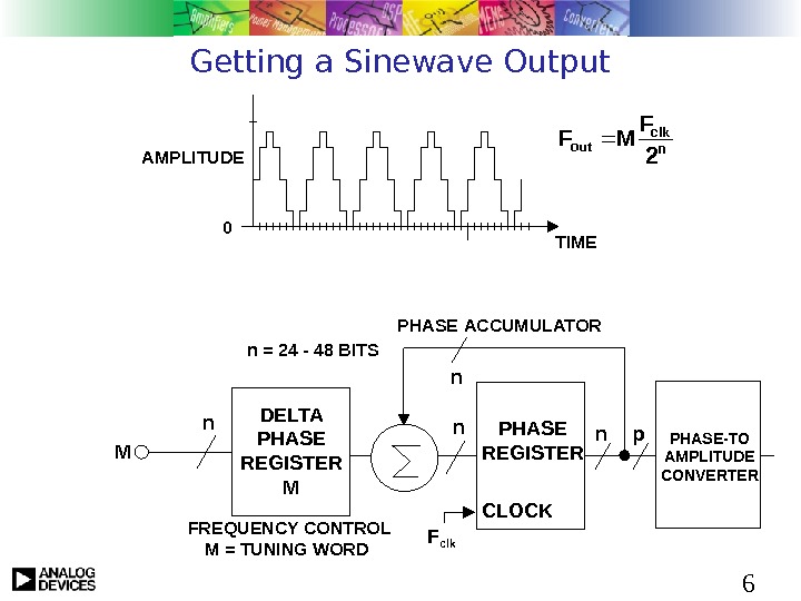
6 Getting a Sinewave Output AMPLITUDE TIME 0 n clk out 2 F MF n. PHASE REGISTER CLOCKn. PHASE ACCUMULATOR nn = 24 — 48 BITS FREQUENCY CONTROL M = TUNING WORD DELTA PHASE REGISTER Mn M F clk PHASE-TO AMPLITUDE CONVERTERp
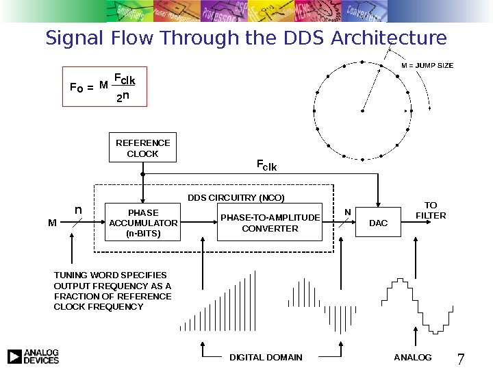
7 Signal Flow Through the DDS Architecture REFERENCE CLOCK PHASE ACCUMULATOR (n — BITS) PHASE — TO — AMPLITUDE CONVERTER DAC M TUNING WORD SPECIFIES OUTPUT FREQUENCY AS A FRACTION OF REFERENCE CLOCK FREQUENCY DIGITAL DOMAIN ANALOGNDDS CIRCUITRY (NCO) TO FILTER 2 n=F o M F clk n
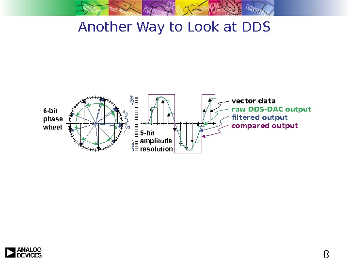
8 Another Way to Look at DDS 6 -bit phase wheel 0 12 34 63… … 02431 29 … … 5 -bit amplitude resolution vector data raw DDS-DAC output filtered output compared output
The World Leader in High-Performance Signal Processing Solutions 1. Theory (why & how it works) 2. Error Sources 3. Advanced DDS Capabilities 4. Applications Examples Direct Digital Synthesis Theory & Applications paul. smith@analog. com
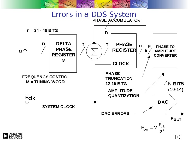
10 Errors in a DDS System PHASE ACCUMULATOR F clk nn FREQUENCY CONTROL M = TUNING WORD PHASE REGISTERDELTA PHASE REGISTER M CLOCKn nn PHASE TRUNCATION 12 -19 BITS N-BITS (10 -14)n = 24 — 48 BITS PHASE-TO AMPLITUDE CONVERTER SYSTEM CLOCK F out. AMPLITUDE QUANTIZATION p M nclk out 2 F MFDAC ERRORS
11 Amplitude Errors Quantized waveform ≠ Sinewave Therefore there will be spectral components 6. 02 N + 1. 76 quantization noise is only valid when clock and data are uncorrelated. NOT THE CASE for a DDS! DAC non-linearities INL and DNL spurs will alias Harmonics from the analog output stage will NOT alias
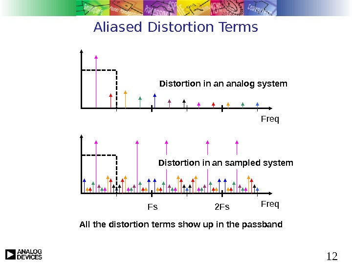
12 Aliased Distortion Terms Freq. Distortion in an analog system Freq Fs 2 Fs. Distortion in an sampled system All the distortion terms show up in the passband
13 Effects of Choosing an Odd Value For M PHASE TIME 2 n -1 0 M=4 PHASE TIME 2 n -1 0 M=
14 Effect Sampling Clock / Output Frequency Ratio on SFDR for Ideal 12 -bit DAC (A) F OUT = 2. 0000 MHz, f S = 80. 0000 MHz FFT SIZE = 8192 THEORETICAL 12 -BIT SNR = 74 d. B FFT PROCESS GAIN = 36 d. B = 10 log(8192/2) FFT NOISE FLOOR = 110 d. BFSSFDR = 77 d. Bc SFDR = 94 d. Bc Ratio = 80/2 = 40 Ratio = 80/2. 0117 = 103/4096(B) F OUT = 2. 0117 MHz, f S = 80. 0000 MHz
15 Phase Truncation Errors Green points (outer circle) show n=8 phase accumulator 256 phase steps M=6 in this illustration Red points (inner circle) show p=5 32 steps passed on the phase-amplitude converter 3 points get truncated, but the 1 st and 4 th do not As the phase moves around the circle, the error becomes periodic Phase error = Amplitude error Due to phase-amplitude converter Periodic phase error = periodic amplitude error = spectral component
16 Phase Truncation Error (Time Domain) Not only is the error periodic, but it also has a ramp shape Therefore we expect the spectral components fall at a 1/m rate (m = harmonic number)
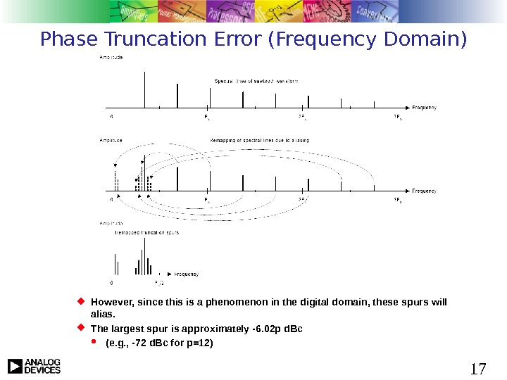
17 Phase Truncation Error (Frequency Domain) However, since this is a phenomenon in the digital domain, these spurs will alias. The largest spur is approximately -6. 02 p d. Bc (e. g. , -72 d. Bc for p=12)
The World Leader in High-Performance Signal Processing Solutions 1. Theory (why & how it works) 2. Error Sources 3. Advanced DDS Capabilities 4. Applications Examples Direct Digital Synthesis Theory & Applications paul. smith@analog. com
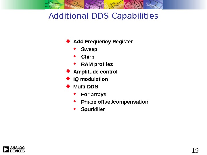
19 Additional DDS Capabilities Add Frequency Register Sweep Chirp RAM profiles Amplitude control IQ modulation Multi-DDS For arrays Phase offset/compensation Spurkiller
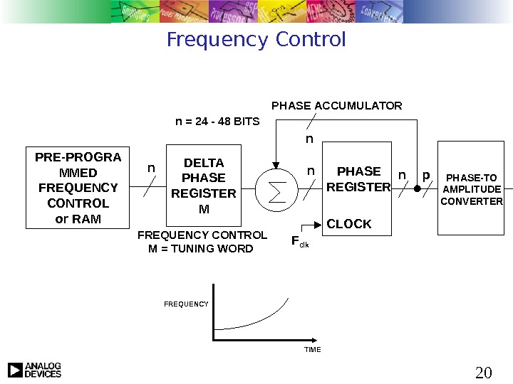
20 Frequency Control n. PHASE REGISTER CLOCKn. PHASE ACCUMULATOR nn = 24 — 48 BITS FREQUENCY CONTROL M = TUNING WORD DELTA PHASE REGISTER Mn F clk PHASE-TO AMPLITUDE CONVERTERp MPRE-PROGRA MMED FREQUENCY CONTROL or RAM TIMEFREQUENCY
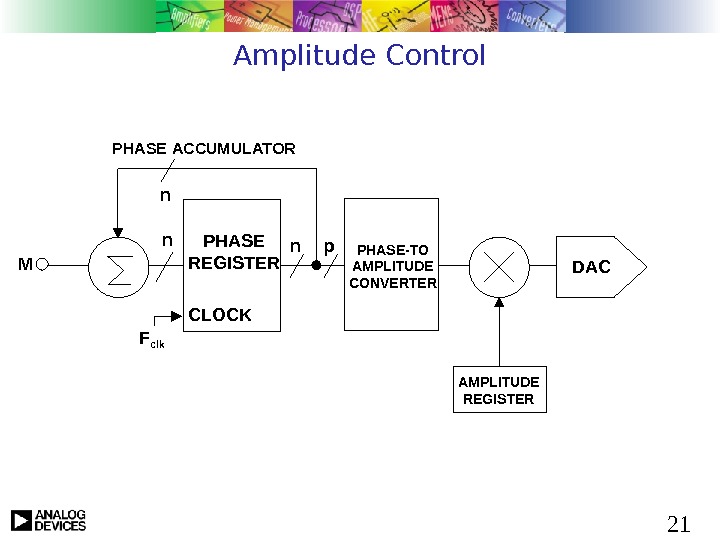
21 Amplitude Control n. PHASE REGISTER CLOCKn. PHASE ACCUMULATOR n F clk PHASE-TO AMPLITUDE CONVERTERp M DAC AMPLITUDE REGISTER
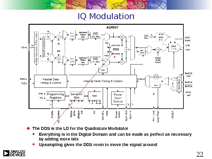
22 IQ Modulation The DDS is the LO for the Quadrature Modulator Everything is in the Digital Domain and can be made as perfect as necessary by adding more bits Upsampling gives the DDS room to move the signal around
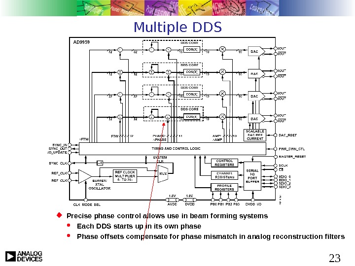
23 Multiple DDS Precise phase control allows use in beam forming systems Each DDS starts up in its own phase Phase offsets compensate for phase mismatch in analog reconstruction filters
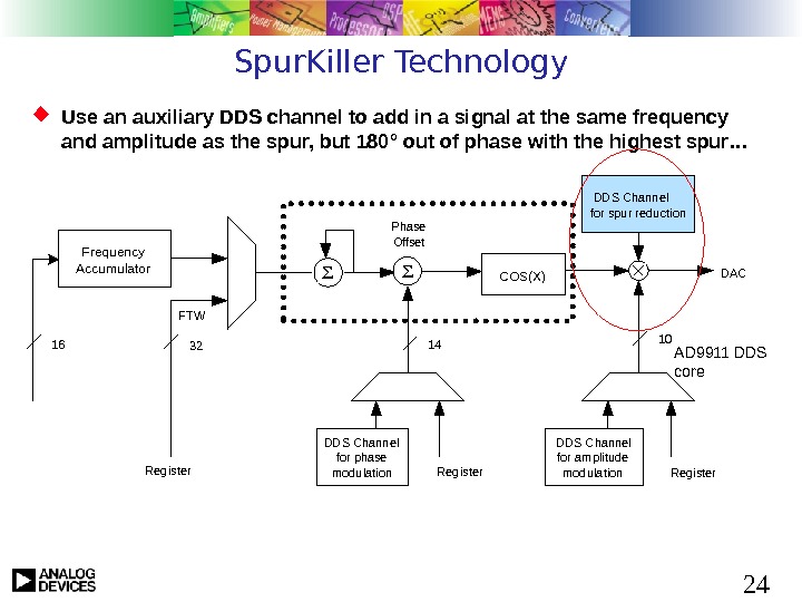
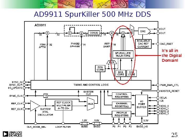
24 COS(X) FTWFrequency Accumulator Phase Offset 14 3216 10 DACDDS Channel for spur reduction DDS Channel for amplitude modulation. DDS Channel for phase modulation. Register. Spur. Killer Technology Use an auxiliary DDS channel to add in a signal at the same frequency and amplitude as the spur, but 180 ° out of phase with the highest spur… AD 9911 DDS core
25 AD 9911 Spur. Killer 500 MHz DDS It’s all in the Digital Domain!
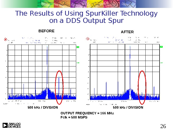
26 The Results of Using Spur. Killer Technology on a DDS Output Spur OUTPUT FREQUENCY = 166 MHz Fclk = 500 MSPS 500 k. Hz / DIVISIONBEFORE AFTER
The World Leader in High-Performance Signal Processing Solutions 1. Theory (why & how it works) 2. Error Sources 3. Advanced DDS Capabilities 4. Applications Examples Direct Digital Synthesis Theory & Applications paul. smith@analog. com
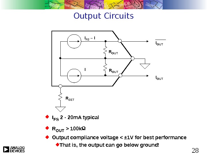
28 Output Circuits R OUTI FS – I I I OUT R SET I FS 2 — 20 m. A typical R OUT > 100 k Output compliance voltage < ± 1 V for best performance That is, the output can go below ground!
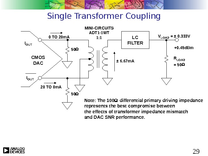
29 Single Transformer Coupling LC FILTERMINI-CIRCUITS ADT 1 -1 WT 1: 1 R LOAD = 50 V LOAD = ± 0. 333 V I OUT 0 TO 20 m. A 20 TO 0 m. A ± 6. 67 m. ACMOS DAC 50 50 +0. 45 d. Bm Note: The 100 differential primary driving impedance represents the best compromise between the effects of transformer impedance mismatch and DAC SNR performance.
30 Dual Transformer Coupling Transmission Line Transformer in series with outputs to help cancel HD 2 Dual Transformer design helps minimize imbalance caused by mis-matched signal coupling from primary to secondary windings. RF Transformer from Coilcraft (TTWB-1 -B) shows better performance for IFs at 200 -300 MHz CMOS DAC 50 Mini-Circuits ADTL 1 -12 Coilcraft TTWB-1 -B TO 50 LOAD 20 -1200 MHz 0. 13 -425 MHz V LOAD = ± 0. 333 V +0. 45 d. Bm 0 TO 20 m. A 20 TO 0 m.
31 Differential DC Coupling Using a Dual-Supply Op Amp I OUT 0 TO 20 m. A 20 TO 0 m. ACMOS DAC AD 8055 +– +5 V – 5 V 25 25 0 V TO +0. 5 V TO 0 V C FILTER 500 1000 ± 1 V f 3 d. B = 1 2 • 50 • C FILTER OR
32 Differential DC Coupling Using a Single-Supply Op Amp I OUT 0 TO 20 m. A 20 TO 0 m. ACMOS DAC AD 8061 +– +5 V 25 25 0 V TO +0. 5 V TO 0 V C FILTER 500 2 k 1 k ± 1 V+2. 5 V +5 V 2 k f 3 d. B = 1 2 • 50 • C FILTER
33 High-Speed Buffered Differential DAC Outputs I OUT CMOS DAC + – AD 813 x ADA 493 x. V OCM 2. 49 k 5 V p-p DIFFERENTIAL OUTPUT 0 TO 20 m. A 20 TO 0 m. A 0 V TO +0. 5 V TO 0 V 25 25 f 3 d. B = 1 2 • 50 • C FILTER
34 Generating a Clock With a DDS Limiter Reconstruction Filter. Fsysclock(fc) DAC out Filter out Clock out Ideal Time Domain Response Ideal Frequency Domain Response «Real World» Frequency Response t 0 1 1 3 5 7 Odd harmonic series 1 3 5 7 t t f ff fc fc 2 fc. DDS External filtering removes unwanted images A squaring circuit converts the signal back to a digital clock
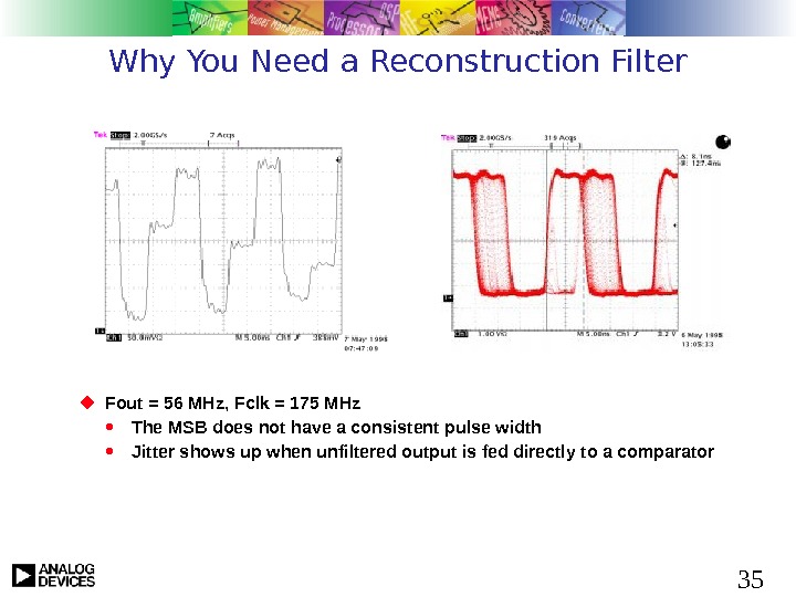
35 Why You Need a Reconstruction Filter Fout = 56 MHz, Fclk = 175 MHz The MSB does not have a consistent pulse width Jitter shows up when unfiltered output is fed directly to a comparator
36 AN-823 Discusses DDS-based Clocks With Very Low Phase Noise Phase noise floor below – 150 d. Bc/Hz Power dissipation <200 m. W per channel 15. 1 MHz 40. 1 MHz 75. 1 MHz 100. 3 MHz. REF CLOCK = 500 MHz, MULTIPLIER DISABLED 100. 3 MHz 75. 1 MHz 40. 1 MHz 15. 1 MHz
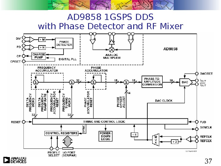
37 AD 9858 1 GSPS DDS with Phase Detector and RF Mixer
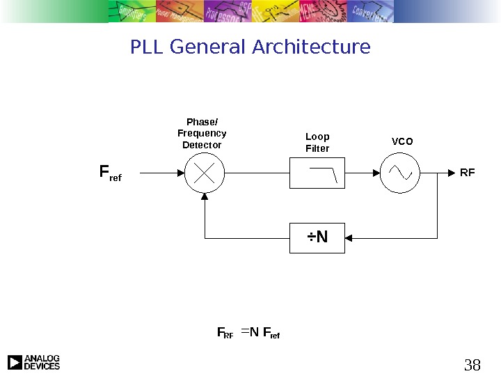
38 PLL General Architecture RF ÷NLoop Filter VCOPhase/ Frequency Detector F ref. RF FN
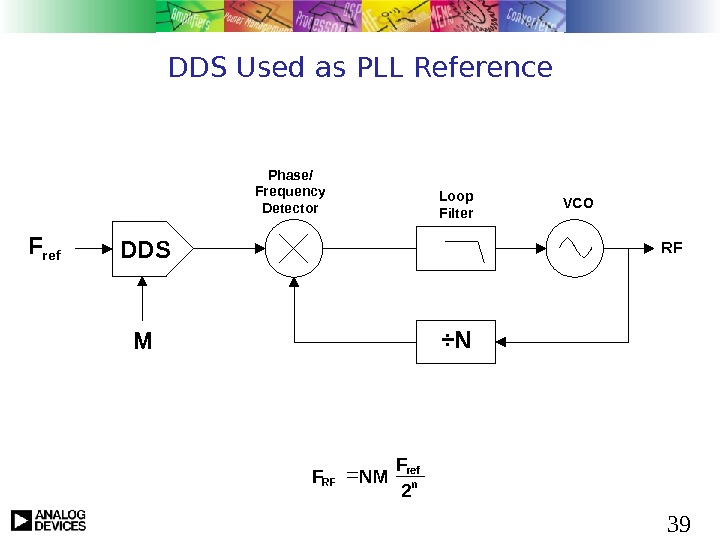
39 DDS Used as PLL Reference RF ÷NLoop Filter VCOPhase/ Frequency Detector F ref DDS nref RF 2 F NMF M
40 DDS Used in Fractional-N Loop RFLoop Filter VCOPhase/ Frequency Detector F ref DDS ref RF n 2 F MF M
41 DDS Used in Translation Loop RFLoop Filter VCOPhase/ Frequency Detector F ref DDS÷N n 2 clk. F M ref. RF FNF F clk
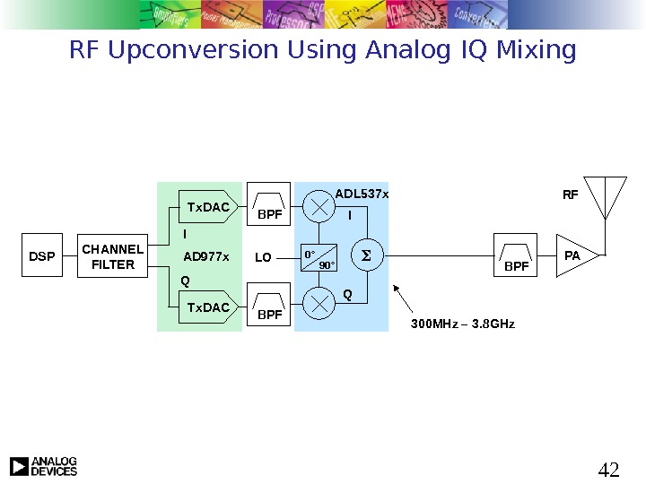
42 RF Upconversion Using Analog IQ Mixing DSP CHANNEL FILTER Tx. DAC BPF PARF LO I Q 0° 90° Tx. DAC BPFAD 977 x ADL 537 x 300 MHz – 3. 8 GHz
43 RF Upconversion Using Digital IQ Mixing DSP CHANNEL FILTER DAC BPF PARF I Q 0° 90°N N BPFNCOQDUC = QUADRATURE DIGITAL UPCONVERTER AD 9857 AD 9957 IF TO 400 MHz (AD 9957) LO
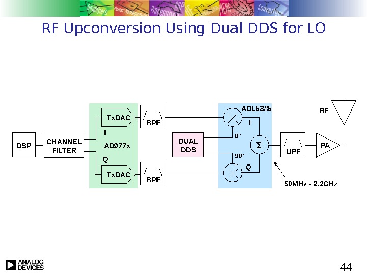
44 RF Upconversion Using Dual DDS for LO DSP CHANNEL FILTER Tx. DAC BPF PARF I Q 0° 90° Tx. DAC BPFAD 977 x ADL 5385 50 MHz — 2. 2 GHz. DUAL DDS
45 On-Line DDS Tools ADIsim. DDS
46 DDS Design Tool Main Screen
47 DDS Design Tool: Tabular Display of Spurs
48 DDS Design Tool: Display Options and Filter Selection
49 http: //www. analog. com/dds Click ‘More …’ to find the cool technical papers
50 Summary DDS can be used to obtain a variety of precision waveforms Compared to other frequency generating techniques, a DDS has the following advantages: Precise phase control without affecting frequency Precise frequency control without affecting phase Fast arbitrary phase changes Fast arbitrary frequency changes Precision modulation DDS has well known error characteristics Care must be taken designing the output analog circuitry Applications abound! ADI makes some GREAT parts