e4b5acc455b88076122636a9beda0628.ppt
- Количество слайдов: 32
 The Vertex Detector at the Factory Valerio Re INFN Pavia and University of Bergamo on behalf of the Super. B collaboration Vertical Integration Workshop Schloss Ringberg, April 6 -9, 2008 V. Re Vertical Integration Workshop, Schloss Ringberg, April 6 – 9, 2008 1
 Outline • The Super. B Project • Vertex Detector Design Issues • Viable options for Layer 0: – Striplets, CMOS Monolithic Active Pixels, Hybrid Pixels • Status of the R&D on Layer 0 options • Conclusions & Perspectives V. Re Vertical Integration Workshop, Schloss Ringberg, April 6 – 9, 2008 2
 Introduction • Flavour physics is rich, promises sensitivity to New Physics – Physics case established and clear, . . . but large statistics (50 -100 ab-1) is needed • Present B-Factories (PEP-II and KEKB) integrated 1. 2 ab-1, exceeding their design goals, with peak Luminosity ~1. 2 -1. 7 x 1034 cm -2 s-1. . . but an upgrade of 1 -2 orders of magnitude in Luminosity is needed to get 50 ab-1 • Increasing Luminosity by raising the current of PEP-II/KEKB is expensive and difficult – wall plug power and detector background explosion – effective limitation around 5 x 1035 cm-2 s-1 • Alternative approach for a Super. B design, exploiting ILC R&D, presented for the first time at Hawaii workshop in March 2005. • After several optimizations we have a Super. B design based on 4 and 7 Ge. V rings (similar to test damping rings for ILC) with moderate currents (~2 A) and final focus (ILC-like) L=1036 cm-2 s-1 – This approach allows to (re-) use existing detectors and machine components. V. Re Vertical Integration Workshop, Schloss Ringberg, April 6 – 9, 2008 3
 The Super. B Process • • • International Super. B Study Group on – Physics case, Machine, Detector International steering committee established, chaired by M. Giorgi. Members from – Canada, France, Germany, Italy, Russia, Spain, UK, US – Close collaboration with Japan, although not formalized Regular workshops – Five workshops held at SLAC, Paris, Frascati – Super. B Meeting at Daresbury – Two Accelerator retreats at SLAC Conceptual Design Report – Published in March 2007 – Describes Physics case, Accelerator, Detector, including costs International Review Committee appointed by INFN to review CDR – Preliminary report by end of 2007 – Final report in Spring 2008 More information: www. pi. infn. it/Super. B V. Re Vertical Integration Workshop, Schloss Ringberg, April 6 – 9, 2008 4
 Super. B Detector Babar and Belle designs have proven to be very effective for B-Factory physics q q Follow the same ideas for Super. B detector Try to reuse same components as much as possible Main issues: q Machine backgrounds – somewhat larger than in Babar/Belle n q Beam energy asymmetry – a bit smaller n q affects mainly SVT layer 0 design smaller bean pipe and improved SVT resolution needed to preserve vertex z reconstruction performance Strong interaction with machine design More details in: q q V. Re http: //www-conf. slac. stanford. edu/super. B 2008/default. asp - SLAC Detector R&D Workshop (Feb. 14 – 16, 2008) https: //agenda. infn. it/conference. Display. py? conf. Id=163 – Review (Nov 12 -13, 2007) Vertical Integration Workshop, Schloss Ringberg, April 6 – 9, 2008 5
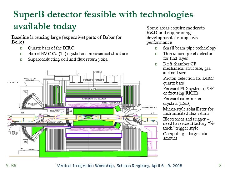 Super. B detector feasible with technologies available today Some areas require moderate Baseline is reusing large (expensive) parts of Babar (or Belle) q q q Quartz bars of the DIRC Barrel EMC Cs. I(Tl) crystal and mechanical structure Superconducting coil and flux return yoke. R&D and engineering developments to improve performance q q q q q V. Re Small beam pipe technology Thin silicon pixel detector first layer Drift chamber CF mechanical structure, gas and cell size Photon detection for DIRC quartz bars Forward PID system (TOF or focusing RICH) Forward calorimeter crystals (LSO) Minos-style scintillator for Instrumented flux return Electronics and trigger – need to revise Bfactory “½track” trigger style Computing – large data amount Vertical Integration Workshop, Schloss Ringberg, April 6 – 9, 2008 6
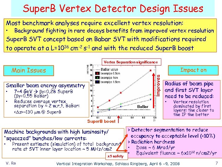 Super. B Vertex Detector Design Issues Most benchmark analyses require excellent vertex resolution: • Background fighting in rare decays benefits from improved vertex resolution Super. B SVT concept based on Babar SVT with modifications required to operate at a L=1036 cm-2 s-1 and with the reduced Super. B boost Vertex Separation significance Main Issues Improves Impact on Smaller beam energy asymmetry • • 7+4 Ge. V bg=0. 28 Super. B (bg=0. 55 Ba. Bar) Reduces average vertex separation by ~ 2 w. r. t. Bar:
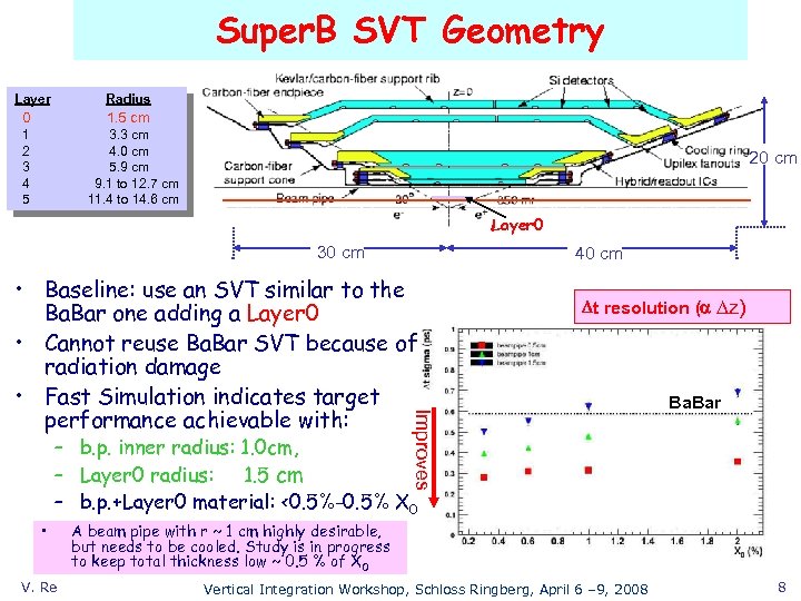 Super. B SVT Geometry Layer Radius 0 1. 5 cm 1 2 3 4 5 3. 3 cm 4. 0 cm 5. 9 cm 9. 1 to 12. 7 cm 11. 4 to 14. 6 cm 20 cm Layer 0 30 cm 40 cm Dt resolution (a Dz) Improves • Baseline: use an SVT similar to the Ba. Bar one adding a Layer 0 • Cannot reuse Ba. Bar SVT because of radiation damage • Fast Simulation indicates target performance achievable with: Ba. Bar – b. p. inner radius: 1. 0 cm, – Layer 0 radius: 1. 5 cm – b. p. +Layer 0 material: <0. 5%-0. 5% X 0 • V. Re A beam pipe with r ~ 1 cm highly desirable, but needs to be cooled. Study is in progress to keep total thickness low ~ 0. 5 % of X 0 Vertical Integration Workshop, Schloss Ringberg, April 6 – 9, 2008 8
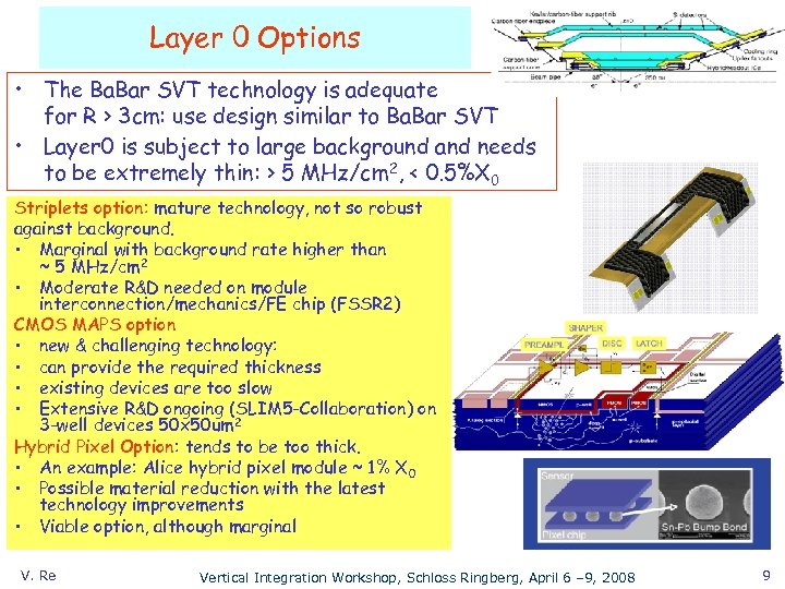 Layer 0 Options • The Ba. Bar SVT technology is adequate for R > 3 cm: use design similar to Ba. Bar SVT • Layer 0 is subject to large background and needs to be extremely thin: > 5 MHz/cm 2, < 0. 5%X 0 Striplets option: mature technology, not so robust against background. • Marginal with background rate higher than ~ 5 MHz/cm 2 • Moderate R&D needed on module interconnection/mechanics/FE chip (FSSR 2) CMOS MAPS option • new & challenging technology: • can provide the required thickness • existing devices are too slow • Extensive R&D ongoing (SLIM 5 -Collaboration) on 3 -well devices 50 x 50 um 2 Hybrid Pixel Option: tends to be too thick. • An example: Alice hybrid pixel module ~ 1% X 0 • Possible material reduction with the latest technology improvements • Viable option, although marginal V. Re Vertical Integration Workshop, Schloss Ringberg, April 6 – 9, 2008 9
 SLIM 5 -Silicon detectors with Low Interactions with Material • Basic R&D for Layer 0 (CMOS MAPS and thin strips) started in 2004 within the SLIM 5 Collaboration. – Several Italian Institutions involved in the project: • BO, PI (coordination), PV-BG, TO, TN, TS. – R&D project supported by the INFN and the Italian Ministry for Education, University and Research. SLIM 5 Purpose: develop technology for thin silicon tracker systems (sensor/ readout/ support structure/ cooling) crucial to reduce multiple scattering effects for future collider experiments (Super. B, ILC) Realize a demonstration thin silicon tracker with LVL 1 trigger capabilities: • CMOS monolithic active pixels • Thin strip detectors on high resistivity silicon • Associative memory system for track trigger SLIM 5 Project • Low mass mechanical support and services Test beam foreseen in 2008 to measure rate capability, efficiency, resolution V. Re Vertical Integration Workshop, Schloss Ringberg, April 6 – 9, 2008 10
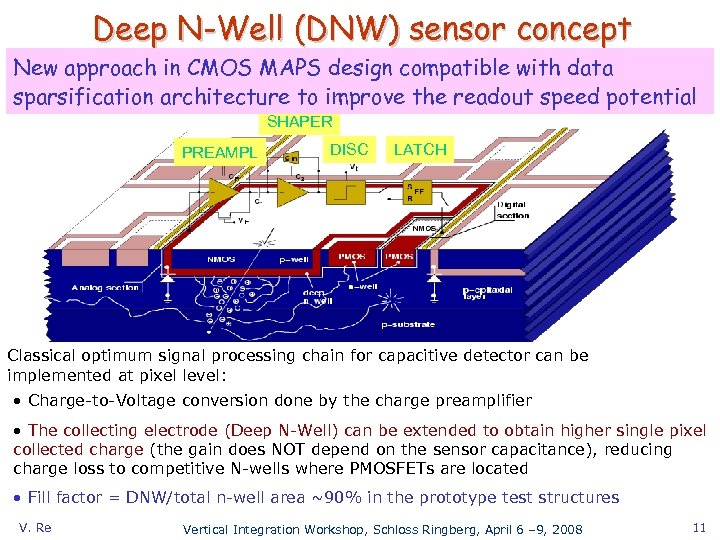 Deep N-Well (DNW) sensor concept New approach in CMOS MAPS design compatible with data sparsification architecture to improve the readout speed potential SHAPER PREAMPL DISC LATCH Classical optimum signal processing chain for capacitive detector can be implemented at pixel level: • Charge-to-Voltage conversion done by the charge preamplifier • The collecting electrode (Deep N-Well) can be extended to obtain higher single pixel collected charge (the gain does NOT depend on the sensor capacitance), reducing charge loss to competitive N-wells where PMOSFETs are located • Fill factor = DNW/total n-well area ~90% in the prototype test structures V. Re Vertical Integration Workshop, Schloss Ringberg, April 6 – 9, 2008 11
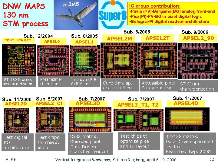 SLIM 5 DNW MAPS 130 nm STM process IC group contribution: • Pavia (PV)-Bergamo(BG) analog front-end • Pisa(PI)-PV-BG in pixel digital logic • Bologna-PI digital readout architecture Sub. 12/2004 Sub. 8/2006 APSEL 2 T APSEL 2 M Sub. 8/2005 TEST_STRUCT APSEL 0 APSEL 1 ST 130 Process characterization Preamplifier characteriz. Improved F-E 8 x 8 Matrix Sub. 11/2006 Sub. 5/2007 Cure thr disp. and induction APSEL 2 D APSEL 2_CT Sub. 7/2007 APSEL 3 D Test digital RO architecture Test chips for shield, xtalk 8 x 32 matrix. Shielded pixel Data Driven sparsified readout V. Re Sub. 9/2006 APSEL 2_90 Accessible pixel Study pix resp. Sub. 7/2007 APSEL 3_T 1, T 2 Test chips to optimize pixel and FE layout ST 90 nm characterization Sub. 11/2007 APSEL 4 D 32 x 128 matrix. Data Driven sparsified readout Beam test Sep. 2008 Vertical Integration Workshop, Schloss Ringberg, April 6 – 9, 2008 12
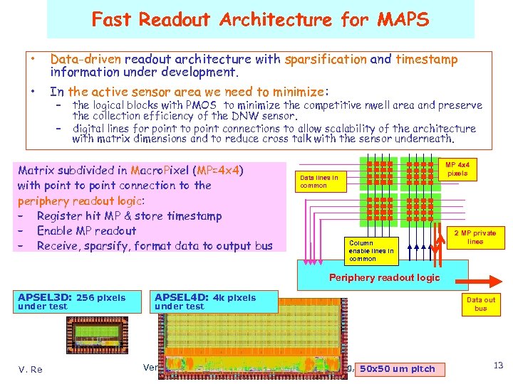 Fast Readout Architecture for MAPS • Data-driven readout architecture with sparsification and timestamp information under development. • In the active sensor area we need to minimize: – – the logical blocks with PMOS to minimize the competitive nwell area and preserve the collection efficiency of the DNW sensor. digital lines for point to point connections to allow scalability of the architecture with matrix dimensions and to reduce cross talk with the sensor underneath. Matrix subdivided in Macro. Pixel (MP=4 x 4) with point to point connection to the periphery readout logic: – Register hit MP & store timestamp – Enable MP readout – Receive, sparsify, format data to output bus MP 4 x 4 pixels Data lines in common Column enable lines in common 2 MP private lines Periphery readout logic APSEL 3 D: 256 pixels under test V. Re APSEL 4 D: 4 k pixels under test Vertical Integration Workshop, Schloss Ringberg, April 6 – 9, 2008 50 x 50 um pitch Data out bus 13
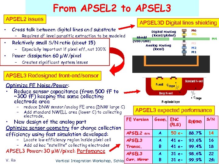 From APSEL 2 to APSEL 3 APSEL 2 issues • • • APSEL 3 D Digital lines shielding Cross talk between digital lines and substrate – Requires a. F level parasitic extraction to be modeled Relatively small S/N ratio (about 15) – Especially important if pixel eff. not 100% Digital routing (local/global) Shield (VDD/GND) Analog routing (local) Power dissipation 60 m. W/pixel – M 6 M 5 M 4 M 3 M 2 M 1 Creates significant system issues APSEL 3 Redesigned front-end/sensor Optimize FE Noise/Power: • Reduce sensor capacitance (from 500 f. F to ~300 f. F) keeping the same collecting electrode area – – reduce DNW sensor/analog FE area (DNW large C) Add standard NWELL area (lower C) to collecting electrode. • New design of the analog part Optimize sensor geometry for charge collection efficiency using fast simulation developed: – – FE Version e(@5 s) S/N 50 e- 88. 7% 14 A B 41 e- 93. 6% 99. 4% 16 18 A 31 e. Curr. Mirror 31 Vertical Integration Workshop, Schloss Ringberg, April 6 B – 9, 2008 e- 98. 6% 99. 9% 22 24 14 Locate low efficiency region inside pixel cell Add ad hoc “satellite” collecting electrodes APSEL 2 Geom. ENC (PLS) A APSEL 3 Power=30 m. W/pixel: Perfomance V. Re APSEL 3 expected performance APSEL 3 Transc. APSEL 3 data
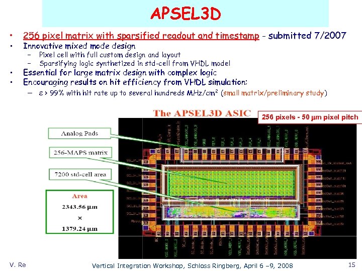 APSEL 3 D • • 256 pixel matrix with sparsified readout and timestamp - submitted 7/2007 Innovative mixed mode design – – Pixel cell with full custom design and layout Sparsifying logic synthetized in std-cell from VHDL model Essential for large matrix design with complex logic Encouraging results on hit efficiency from VHDL simulation: – e > 99% with hit rate up to several hundreds MHz/cm 2 (small matrix/preliminary study) 256 pixels - 50 mm pixel pitch V. Re Vertical Integration Workshop, Schloss Ringberg, April 6 – 9, 2008 15
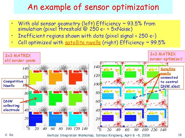 An example of sensor optimization • With old sensor geometry (left) Efficiency ~ 93. 5% from simulation (pixel threshold @ 250 e- = 5 x. Noise) • Inefficient regions shown with dots (pixel signal < 250 e-) • Cell optimized with satellite nwells (right) Efficiency ~ 99. 5% 3 x 3 MATRIX sensor optimized 3 x 3 MATRIX old sensor geom Satellite nwells connected to central DNW elect Competitive Nwells DNW collecting electrode V. Re Vertical Integration Workshop, Schloss Ringberg, April 6 – 9, 2008 16
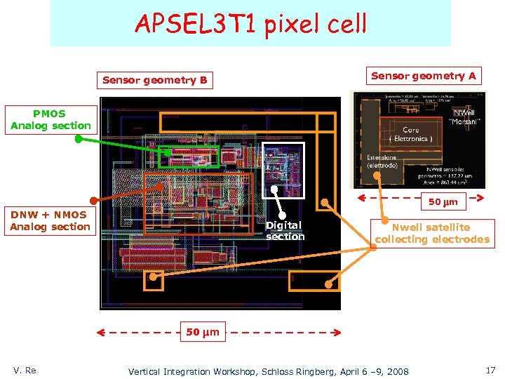 APSEL 3 T 1 pixel cell Sensor geometry A Sensor geometry B PMOS Analog section 50 mm DNW + NMOS Analog section Digital section Nwell satellite collecting electrodes 50 mm V. Re Vertical Integration Workshop, Schloss Ringberg, April 6 – 9, 2008 17
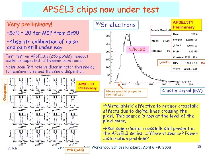 APSEL 3 chips now under test Very preliminary! 90 Sr electrons APSEL 3 T 1 Preliminary • S/N = 20 for MIP from Sr 90 • Absolute calibration of noise and gain still under way S/N=20 First test on APSEL 3 D (256 pixels): readout works as expected…with some bugs found! Landau Noise scan (hit rate vs discriminator threshold) to measure noise and threshold dispersion. Occupancy APSEL 3 D Preliminary Noise events properly normalized m. V Cluster signal (m. V) Metal shield effective to reduce crosstalk effects due to digital lines crossing the pixel. This source is now at the level of the pixel noise… But some digital crosstalk still present in the APSEL 3 series…different source? Power distribution problem? V. Re Vertical Integration Workshop, Schloss Ringberg, April 6 – 9, 2008 Vth (DAC) 18
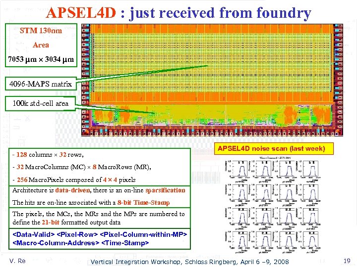 APSEL 4 D : just received from foundry STM 130 nm Area 7053 mm 3034 mm 4096 -MAPS matrix 100 k std-cell area APSEL 4 D noise scan (last week) - 128 columns 32 rows, - 32 Macro. Columns (MC) 8 Macro. Rows (MR), - 256 Macro. Pixels composed of 4 4 pixels Architecture is data-driven, there is an on-line sparsification The hits are on-line associated with a 8 -bit Time-Stamp The pixels, the MCs, the MRs and the MPs are numbered to define the 21 -bit formatted output data
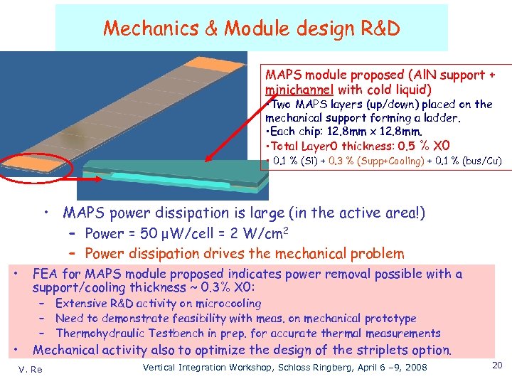 Mechanics & Module design R&D MAPS module proposed (Al. N support + minichannel with cold liquid) • Two MAPS layers (up/down) placed on the mechanical support forming a ladder. • Each chip: 12. 8 mm x 12. 8 mm. • Total Layer 0 thickness: 0. 5 % X 0 • 0. 1 % (Si) + 0. 3 % (Supp+Cooling) + 0. 1 % (bus/Cu) • MAPS power dissipation is large (in the active area!) – Power = 50 μW/cell = 2 W/cm 2 – Power dissipation drives the mechanical problem • • FEA for MAPS module proposed indicates power removal possible with a support/cooling thickness ~ 0. 3% X 0: – Extensive R&D activity on microcooling – Need to demonstrate feasibility with meas. on mechanical prototype – Thermohydraulic Testbench in prep. for accurate thermal measurements Mechanical activity also to optimize the design of the striplets option. V. Re Vertical Integration Workshop, Schloss Ringberg, April 6 – 9, 2008 20
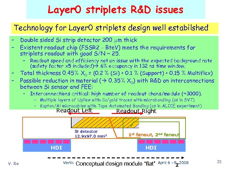 Layer 0 striplets R&D issues Technology for Layer 0 striplets design well estabilshed – – Double sided Si strip detector 200 mm thick Existent readout chip (FSSR 2 - Bte. V) meets the requirements for striplets readout with good S/N ~ 25. – Readout speed and efficiency not an issue with the expected background rate (safety factor x 5 included) 6% occupancy in 132 ns time window. Total thickness 0. 45% X 0 = (0. 2 % (Si) + 0. 1 % (Support) + 0. 15 % Multiflex) Possible reduction in material ( 0. 35% X 0) with R&D on interconnections between Si sensor and FEE: • Interconnections critical: high number of readout chans/module (~3000). – Multiple layers of Upilex with Cu/gold traces with microbonding (as in SVT) – Kapton/Al microcables with Tape Automated Bonding (as in ALICE experiment) Readout Left Si detector 12. 9 x 97. 0 mm 2 HDI V. Re Readout Right 1 st fanout, 2 nd fanout HDI z Vertical Integration Workshop, Schloss Ringberg, April 6 – 9, 2008 Conceptual design module “flat” 21
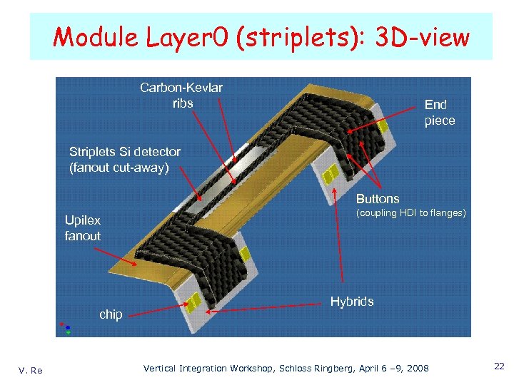 Module Layer 0 (striplets): 3 D-view Carbon-Kevlar ribs End piece Striplets Si detector (fanout cut-away) Buttons Upilex fanout chip V. Re (coupling HDI to flanges) Hybrids Vertical Integration Workshop, Schloss Ringberg, April 6 – 9, 2008 22
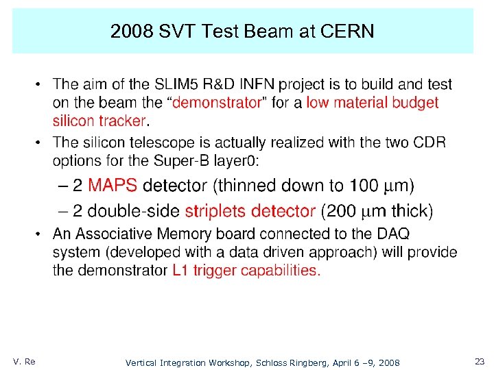 2008 SVT Test Beam at CERN V. Re Vertical Integration Workshop, Schloss Ringberg, April 6 – 9, 2008 23
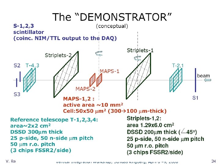 V. Re Vertical Integration Workshop, Schloss Ringberg, April 6 – 9, 2008 24
 Benefits of Vertical Integration • Time to explore new pixel technology for SVT Layer 0? • Can use MAPS readout electronics on a thin chip connected to high resistivity thin pixel sensor? – Improve S/N w. r. t. to CMOS MAPS: • pixels on high resistivity substrate are fully depleted • Signal proportional to sensor thickness • Noise reduced with the lower detector capacitance – Reduce power dissipation (trade off with noise reduction) – Sensor can be extremely radiation hard • Can use CMOS MAPS on 2 tiers? (sensor&analog + digital) • See talk on 3 D activities in Italian HEP labs tomorrow V. Re Vertical Integration Workshop, Schloss Ringberg, April 6 – 9, 2008 25
 Perspectives • There is a growing international interest and participation to the Super. B Project. • The Conceptual Design Report is now under review: – Report by Spring 2008. • Next Super. B steps: from CDR to TDR (~ 2 years → 2010): – Accelerator studies continue to optimize the machine parameters. • Test in Dafne began Nov ’ 07 (crab waist and basic concepts of Super. B IP scheme): so far so good – Detector R&D coordination has been formed (meets every other week) – Physics groups active to update on Physics case (looking at complementarity with LHC). Design and construction: ~ 4 years → 2014 (shorter timescale with respect to ILC and SLHC projects) Super. B could be considered as a “precursor” for next generation experiments (machine & detector) V. Re Vertical Integration Workshop, Schloss Ringberg, April 6 – 9, 2008 26
 Backup V. Re Vertical Integration Workshop, Schloss Ringberg, April 6 – 9, 2008 27
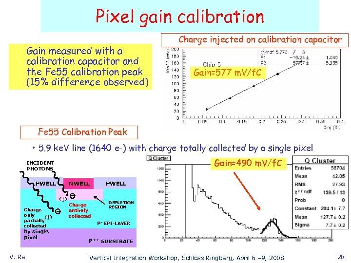 Pixel gain calibration Gain measured with a calibration capacitor and the Fe 55 calibration peak (15% difference observed) Charge injected on calibration capacitor Gain=577 m. V/f. C Fe 55 Calibration Peak • 5. 9 ke. V line (1640 e-) with charge totally collected by a single pixel Gain=490 m. V/f. C INCIDENT PHOTONS PWELL Charge only partially collected by single pixel V. Re NWELL Charge entirely collected PWELL DEPLETION REGION P- EPI-LAYER P++ SUBSTRATE Vertical Integration Workshop, Schloss Ringberg, April 6 – 9, 2008 28
 MAPS Radiation Hardness • Expected Background @ Layer 0: – Dose = 6 Mrad/yr – Equivalent fluence = 6 x 10¹² neq/cm 2/yr • CMOS readout electronics (deep submicron) rad hard • MAPS sensor - Radiation damage affects S/N Results from standard nwell MAPS prototypes • Non-ionizing radiation: bulk damage cause charge collection reduction, due to lower minority carrier lifetime (trapping) fluences ~ 1012 neq/cm 2 affordable, 1013 neq/cm 2 possible • Ionizing radiation: noise increase, due to higher diode leakage current (surface damage) OK up to 20 Mrad with low integration time (10 ms) or T operation < 0 o C, or modified pixel design to improve it • • V. Re Irradiation test performed on several MAPS prototypes, with standard nwell sensor, indicate application for Super. B is viable. APSEL chips irradiation started this summer …. Vertical Integration Workshop, Schloss Ringberg, April 6 – 9, 2008 29
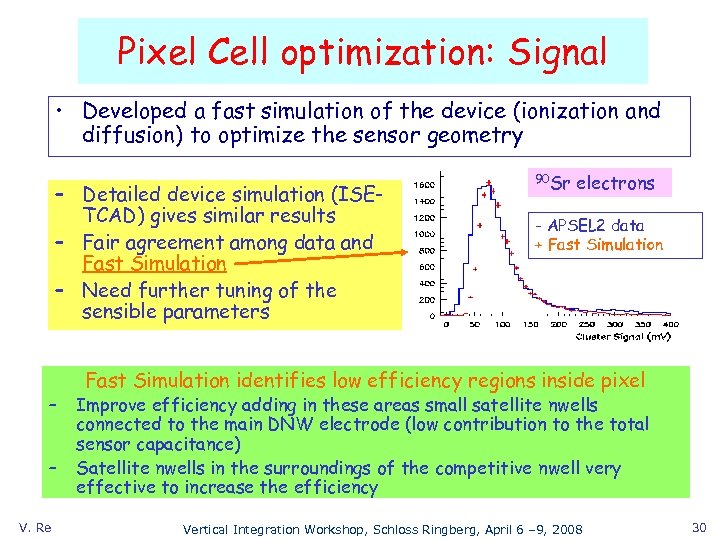 Pixel Cell optimization: Signal • Developed a fast simulation of the device (ionization and diffusion) to optimize the sensor geometry – Detailed device simulation (ISETCAD) gives similar results – Fair agreement among data and Fast Simulation – Need further tuning of the sensible parameters – – V. Re 90 Sr electrons - APSEL 2 data + Fast Simulation identifies low efficiency regions inside pixel Improve efficiency adding in these areas small satellite nwells connected to the main DNW electrode (low contribution to the total sensor capacitance) Satellite nwells in the surroundings of the competitive nwell very effective to increase the efficiency Vertical Integration Workshop, Schloss Ringberg, April 6 – 9, 2008 30
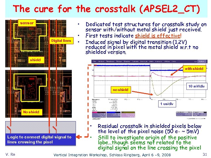 The cure for the crosstalk (APSEL 2_CT) • sensor Digital lines • • Dedicated test structures for crosstalk study on sensor with/without metal shield just received. First tests indicate shield is effective! Induced signal by digital transition (1. 2 V) reduced in pixel with the metal shield w. r. t no shielded version. shield with shield 10 m. V/div no shield 1 us/div No shield • Logic to connect digital signal to lines crossing the pixel V. Re • Residual crosstalk in shielded pixels below the level of the pixel noise (50 e- ~ 5 m. V) Still to investigate origin of the positive lobe…though seems not related to the digital signal on the line crossing the pixel Vertical Integration Workshop, Schloss Ringberg, April 6 – 9, 2008 31
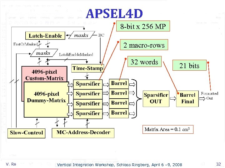 APSEL 4 D 8 -bit x 256 MP 2 macro-rows 32 words 21 bits Matrix Area = 0. 1 cm 2 V. Re Vertical Integration Workshop, Schloss Ringberg, April 6 – 9, 2008 32


