7553545354512.ppt
- Количество слайдов: 8
 The theme of the Ph. D thesis: Visualizing the incipient growth of Zn. O ultra thin films on In. Ga. As for tailoring contact resistivity the project VIGOS The coordinator of the project: Pr. H. Renevier (LMGP) Ph. D student: Eugene Skopin
 Nizhny Novgorod (RUSSIA) -2 - Degree, the time period of study The University Bachelor (Nanotechnology) 2008 -2012 Lobachevsky State University of Nizhny Novgorod (Nizhny Novgorod, Russia), Faculty of physics, Department of solid state electronics. Master (Electronics and Nanoelectronics) 2012 -2014
 The project VIGOS. Partners. 1) Grenoble Institute of Technology / LMGP & SIMa. P H. Renevier, J-L. Deschanvres, E. Blanquet, A. Crisci 2) Leti (Grenoble) O. Renault, F. Nemouchi, F. Bertin 3) IM 2 NP (Université Aix Marseille). O. Thomas, M. I. Richard, C. Guichet, T. Ouled, R. Hayn. 4) SOLEIL Synchrotron (St Aubin) G. Ciatto 5) Dr. D. Fong (Argonne National Laboratory, USA) -3 -
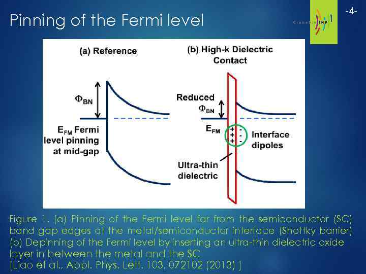 Pinning of the Fermi level -4 - Figure 1. (a) Pinning of the Fermi level far from the semiconductor (SC) band gap edges at the metal/semiconductor interface (Shottky barrier) (b) Depinning of the Fermi level by inserting an ultra-thin dielectric oxide layer in between the metal and the SC [Liao et al. , Appl. Phys. Lett. 103, 072102 (2013) ]
 -5 - The two main work packages The studying of the incipient growth of Zn. O ultra-thin films by atomic layer deposition (ALD) and Pulsed Injected Metal Organic Chemical Vapor Deposition (PIMOCVD) on In. Ga. As substrates and determine the interface structure layer by layer, through the use of in situ characterization techniques, including synchrotron X-ray methods. The studying of the chemical and structural changes of the Zn. O/In. Ga. As stack when covered with the metallic contacts, paying special attention to interfaces.
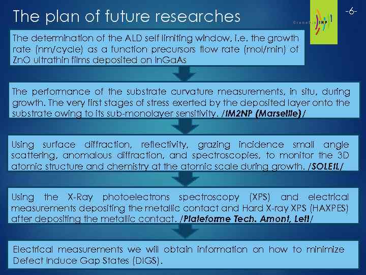 The plan of future researches -6 - The determination of the ALD self limiting window, i. e. the growth rate (nm/cycle) as a function precursors flow rate (mol/min) of Zn. O ultrathin films deposited on In. Ga. As The performance of the substrate curvature measurements, in situ, during growth. The very first stages of stress exerted by the deposited layer onto the substrate owing to its sub-monolayer sensitivity. /IM 2 NP (Marseille)/ Using surface diffraction, reflectivity, grazing incidence small angle scattering, anomalous diffraction, and spectroscopies, to monitor the 3 D atomic structure and chemistry at the atomic scale during growth. /SOLEIL/ Using the X-Ray photoelectrons spectroscopy (XPS) and electrical measurements depositing the metallic contact and Hard X-ray XPS (HAXPES) after depositing the metallic contact. /Plateforme Tech. Amont, Leti/ Electrical measurements we will obtain information on how to minimize Defect Induce Gap States (DIGS).
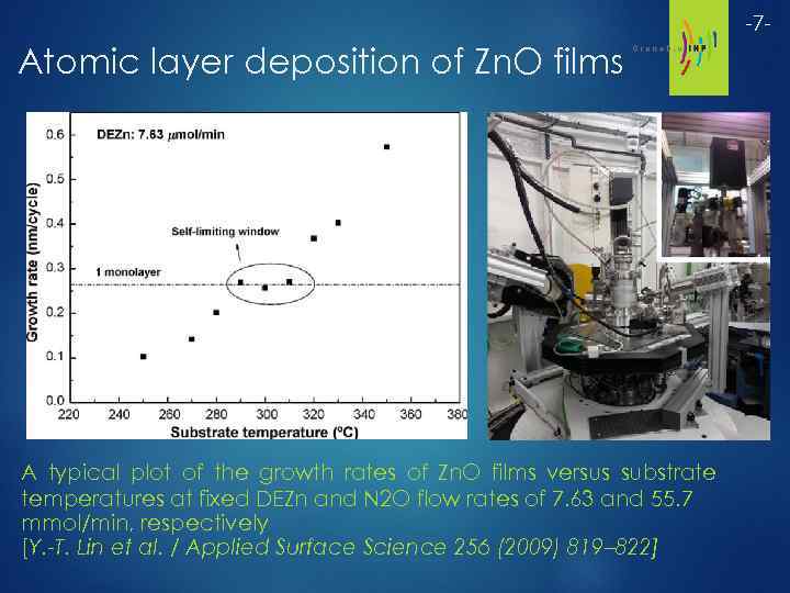 -7 - Atomic layer deposition of Zn. O films A typical plot of the growth rates of Zn. O films versus substrate temperatures at fixed DEZn and N 2 O flow rates of 7. 63 and 55. 7 mmol/min, respectively [Y. -T. Lin et al. / Applied Surface Science 256 (2009) 819– 822]
 Thank you for your attention!


