5287d3a2b5f5f9c691fbb622ad2a7684.ppt
- Количество слайдов: 23
 The S-Altro project An overview and status of the S-Altro project (at CERN). People : L. Musa… Architecture Gerd Trampitsch (no longer at CERN) …. . Front-end Magnus Mager …. PASA characterisation Hugo França …. ADC Eduardo Garcia …. . Signal processing Christian Patauner …. Data compression Presented at the : EUDET Annual Meeting 2008 Nikhef, Amsterdam, October 6 -8 2008 P. Aspell CERN EUDET Annual Meeting, Nikhef, Amsterdam, October 6 -8 2008
 Talk Outline • S-Altro history and objectives • The front-end (Pasa) • ADC • Digital signal processing • Data Compression • Putting it together • Summary P. Aspell CERN EUDET Annual Meeting, Nikhef, Amsterdam, October 6 -8 2008
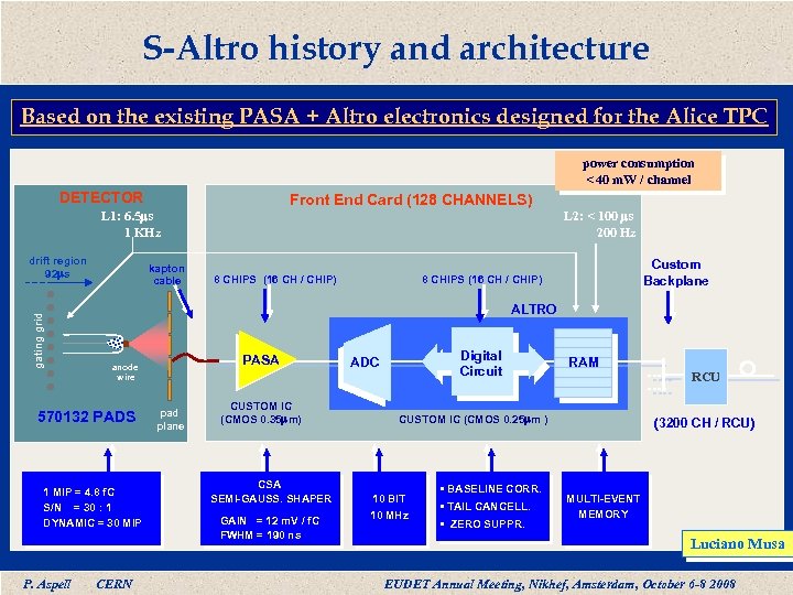 S-Altro history and architecture Based on the existing PASA + Altro electronics designed for the Alice TPC power consumption < 40 m. W / channel DETECTOR Front End Card (128 CHANNELS) L 1: 6. 5 ms 1 KHz gating grid drift region 92 ms kapton cable Custom Backplane 8 CHIPS (16 CH / CHIP) ALTRO PASA anode wire 570132 PADS 1 MIP = 4. 8 f. C S/N = 30 : 1 DYNAMIC = 30 MIP P. Aspell 8 CHIPS (16 CH / CHIP) L 2: < 100 ms 200 Hz CERN pad plane CUSTOM IC (CMOS 0. 35 mm) CSA SEMI-GAUSS. SHAPER GAIN = 12 m. V / f. C FWHM = 190 ns Digital Circuit ADC RAM RCU CUSTOM IC (CMOS 0. 25 mm ) 10 BIT 10 MHz • BASELINE CORR. • TAIL CANCELL. • ZERO SUPPR. (3200 CH / RCU) MULTI-EVENT MEMORY Luciano Musa EUDET Annual Meeting, Nikhef, Amsterdam, October 6 -8 2008
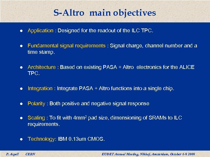 S-Altro main objectives l l Fundamental signal requirements : Signal charge, channel number and a time stamp. l Architecture : Based on existing PASA + Altro electronics for the ALICE TPC. l Integration : Integrate PASA + Altro functions into a single chip. l Polarity : Both positive and negative signal response l Scaling : To fit with 4 mm 2 pad size, dimensioning of SRAMs to ILC requirements. l P. Aspell Application : Designed for the readout of the ILC TPC. Technology: IBM 0. 13 um CMOS. CERN EUDET Annual Meeting, Nikhef, Amsterdam, October 6 -8 2008
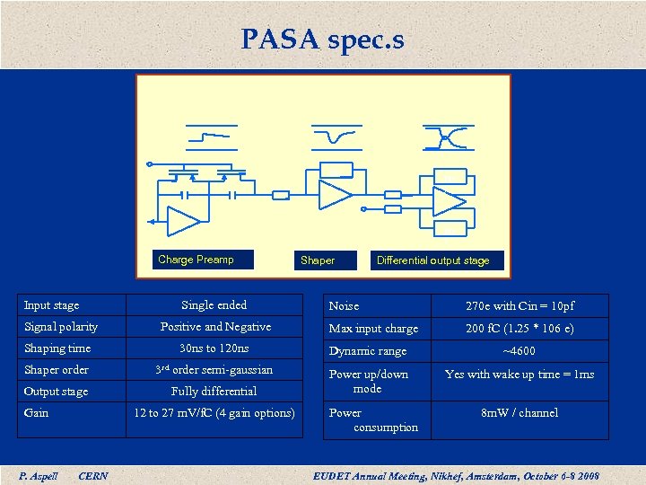 PASA spec. s H(s ) Charge Preamp Input stage Signal polarity Single ended Positive and Negative Shaper Differential output stage Noise 270 e with Cin = 10 pf Max input charge 200 f. C (1. 25 * 106 e) Shaping time 30 ns to 120 ns Dynamic range ~4600 Shaper order 3 rd order semi-gaussian Yes with wake up time = 1 ms Output stage Fully differential Power up/down mode Gain P. Aspell 12 to 27 m. V/f. C (4 gain options) CERN Power consumption 8 m. W / channel EUDET Annual Meeting, Nikhef, Amsterdam, October 6 -8 2008
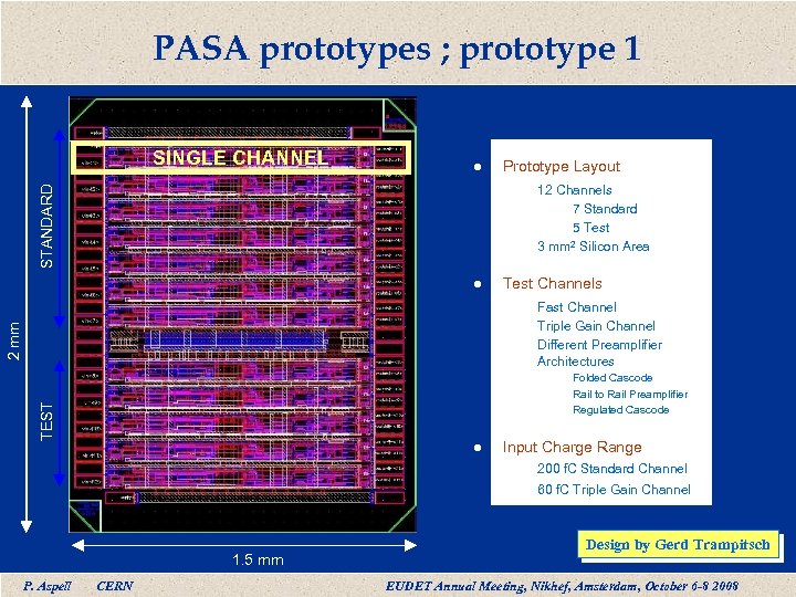 PASA prototypes ; prototype 1 SINGLE CHANNEL l Prototype Layout STANDARD » » l Test Channels 2 mm » » » Fast Channel Triple Gain Channel Different Preamplifier Architectures TEST – – – l 1. 5 mm CERN Folded Cascode Rail to Rail Preamplifier Regulated Cascode Input Charge Range » » P. Aspell 12 Channels – 7 Standard – 5 Test 3 mm 2 Silicon Area 200 f. C Standard Channel 60 f. C Triple Gain Channel Design by Gerd Trampitsch EUDET Annual Meeting, Nikhef, Amsterdam, October 6 -8 2008
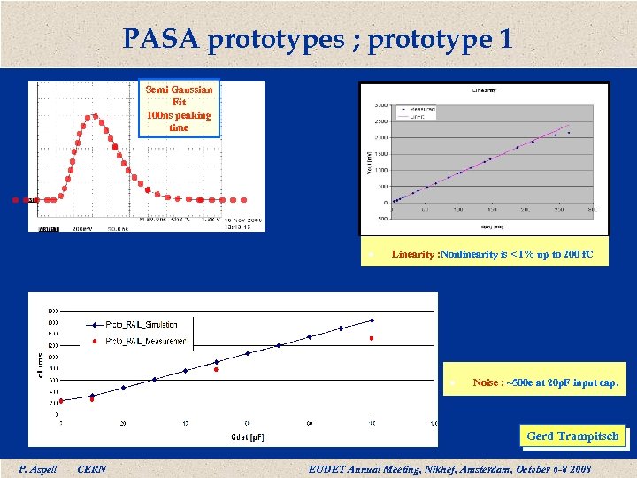 PASA prototypes ; prototype 1 Semi Gaussian Fit 100 ns peaking time l Linearity : Nonlinearity is < 1% up to 200 f. C l Noise : ~500 e at 20 p. F input cap. Gerd Trampitsch P. Aspell CERN EUDET Annual Meeting, Nikhef, Amsterdam, October 6 -8 2008
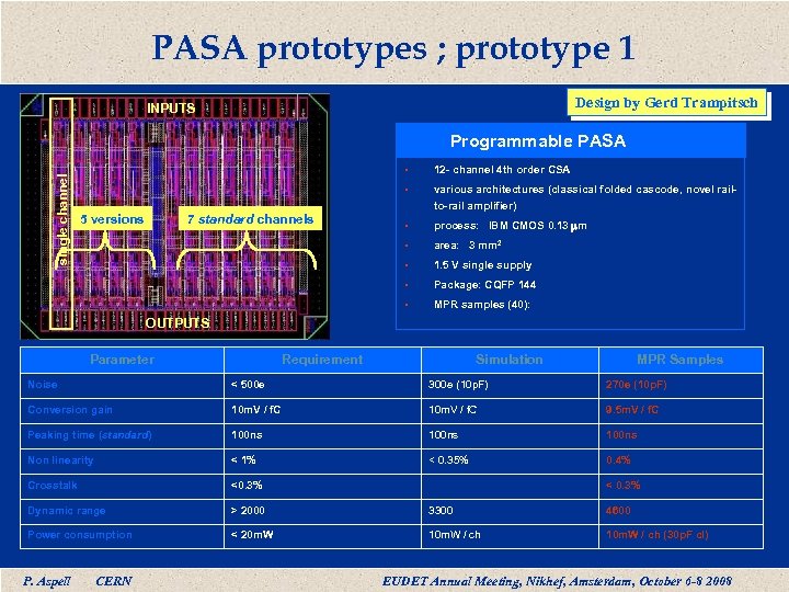 PASA prototypes ; prototype 1 Design by Gerd Trampitsch INPUTS single channel Programmable PASA § § 5 versions 7 standard channels 12 - channel 4 th order CSA various architectures (classical folded cascode, novel railto-rail amplifier) § process: IBM CMOS 0. 13 mm § area: 3 mm 2 § 1. 5 V single supply § Package: CQFP 144 § MPR samples (40): OUTPUTS Parameter Requirement Simulation MPR Samples Noise < 500 e 300 e (10 p. F) 270 e (10 p. F) Conversion gain 10 m. V / f. C 9. 5 m. V / f. C Peaking time (standard) 100 ns Non linearity < 1% < 0. 35% 0. 4% Crosstalk <0. 3% Dynamic range > 2000 3300 4600 Power consumption < 20 m. W 10 m. W / ch (30 p. F cl) P. Aspell CERN < 0. 3% EUDET Annual Meeting, Nikhef, Amsterdam, October 6 -8 2008
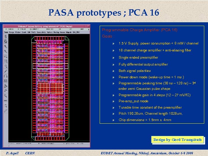 PASA prototypes ; PCA 16 Programmable Charge Amplifier (PCA 16) Goals : » 1. 5 V Supply, power consumption < 8 m. W / channel » 16 channel charge amplifier + anti-aliasing filter » Single ended preamplifier » Fully differential output amplifier » Both signal polarities » Power down mode (wake-up time = 1 ms ) » Programmable peaking time (30 ns – 120 ns) – 3 rd order semi Gaussian pulse shape » Programmable gain in 4 steps (12 – 27 m. V/f. C) » Pre-amp_out mode » Tunable time constant of the preamplifier » Pitch 190. 26 um, Channel length 1026 um, » Chip dimensions = 1. 5 mm x 4 mm Design by Gerd Trampitsch P. Aspell CERN EUDET Annual Meeting, Nikhef, Amsterdam, October 6 -8 2008
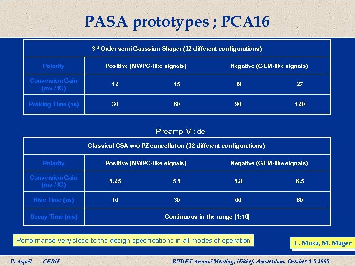 PASA prototypes ; PCA 16 3 rd Order semi Gaussian Shaper (32 different configurations) Polarity Positive (MWPC-like signals) Negative (GEM-like signals) Conversion Gain (mv / f. C) 12 15 19 27 Peaking Time (ns) 30 60 90 120 Preamp Mode Classical CSA w/o PZ cancellation (32 different configurations) Polarity Positive (MWPC-like signals) Negative (GEM-like signals) Conversion Gain (mv / f. C) 5. 25 5. 8 6. 5 Rise Time (ns) 10 30 60 80 Decay Time (ms) Continuous in the range [1: 10] Performance very close to the design specifications in all modes of operation P. Aspell CERN L. Musa, M. Mager EUDET Annual Meeting, Nikhef, Amsterdam, October 6 -8 2008
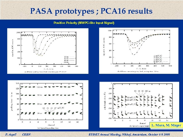 PASA prototypes ; PCA 16 results Positive Polarity (MWPC-like Input Signal) L. Musa, M. Mager P. Aspell CERN EUDET Annual Meeting, Nikhef, Amsterdam, October 6 -8 2008
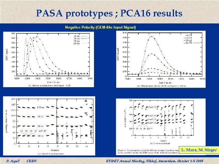 PASA prototypes ; PCA 16 results Negative Polarity (GEM-like Input Signal) L. Musa, M. Mager P. Aspell CERN EUDET Annual Meeting, Nikhef, Amsterdam, October 6 -8 2008
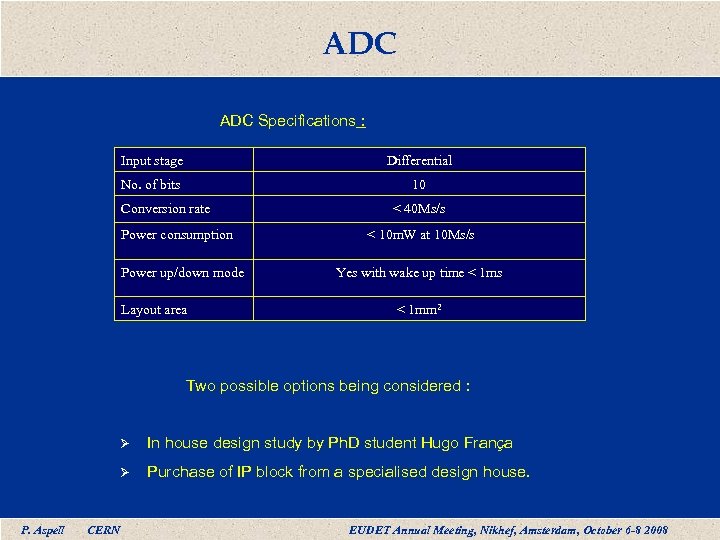 ADC Specifications : Input stage Differential No. of bits 10 Conversion rate Power consumption Power up/down mode Layout area < 40 Ms/s < 10 m. W at 10 Ms/s Yes with wake up time < 1 ms < 1 mm 2 Two possible options being considered : Ø Ø P. Aspell CERN In house design study by Ph. D student Hugo França Purchase of IP block from a specialised design house. EUDET Annual Meeting, Nikhef, Amsterdam, October 6 -8 2008
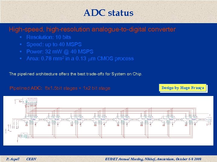 ADC status High-speed, high-resolution analogue-to-digital converter • • Resolution: 10 bits Speed: up to 40 MSPS Power: 32 m. W @ 40 MSPS Area: 0. 78 mm 2 in a 0. 13 µm CMOS process The pipelined architecture offers the best trade-offs for System on Chip. Pipelined ADC: 8 x 1. 5 bit stages + 1 x 2 bit stage P. Aspell CERN Design by Hugo França EUDET Annual Meeting, Nikhef, Amsterdam, October 6 -8 2008
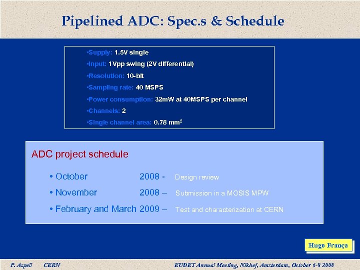 Pipelined ADC: Spec. s & Schedule • Supply: 1. 5 V single • Input: 1 Vpp swing (2 V differential) • Resolution: 10 -bit • Sampling rate: 40 MSPS • Power consumption: 32 m. W at 40 MSPS per channel • Channels: 2 • Single channel area: 0. 78 mm 2 ADC project schedule • October 2008 - Design review • November 2008 – Submission in a MOSIS MPW • February and March 2009 – Test and characterization at CERN Hugo França P. Aspell CERN EUDET Annual Meeting, Nikhef, Amsterdam, October 6 -8 2008
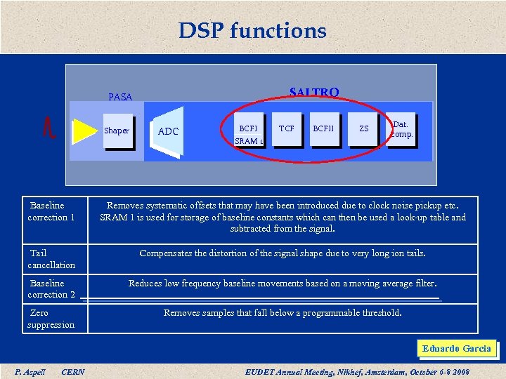 DSP functions SALTRO PASA Shaper ADC BCFI SRAM 1 TCF BCFII ZS Dat. comp. Baseline correction 1 Removes systematic offsets that may have been introduced due to clock noise pickup etc. SRAM 1 is used for storage of baseline constants which can then be used a look-up table and subtracted from the signal. Tail cancellation Compensates the distortion of the signal shape due to very long ion tails. Baseline correction 2 Reduces low frequency baseline movements based on a moving average filter. Zero suppression Removes samples that fall below a programmable threshold. Eduardo Garcia P. Aspell CERN EUDET Annual Meeting, Nikhef, Amsterdam, October 6 -8 2008
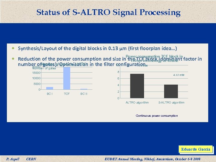 Status of S-ALTRO Signal Processing Synthesis/Layout of the digital blocks in 0. 13 μm (first floorplan idea…) Power consumption TCF block in Reduction of the power consumption and size in the TCF block (dominant factor in 130 nm technology at 40 Mhz number of. Number of Optimization in the filter configuration. gates). gates in ALTRO 10 7. 36 m. W 20000 Number of gates 15000 8 10000 6 5000 4 0 BC I TCF BC II 4. 03 m. W 2 0 ALTRO algorithm S-ALTRO algorithm Continuous power consumption Eduardo Garcia P. Aspell CERN EUDET Annual Meeting, Nikhef, Amsterdam, October 6 -8 2008
 Optimising for low power Low power Design: Circuit level optimization (Reducing VDD has a quadratic effect on Pdyn) Study of the relationship Power Vs Delay Study/Design of the filters taking account the timing of the low power system. For example: feedback in the TCF block… Eduardo Garcia P. Aspell CERN EUDET Annual Meeting, Nikhef, Amsterdam, October 6 -8 2008
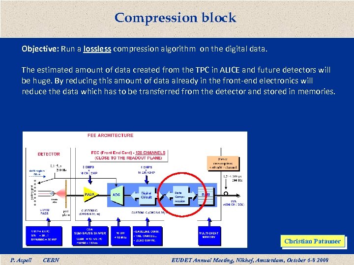 Compression block Objective: Run a lossless compression algorithm on the digital data. The estimated amount of data created from the TPC in ALICE and future detectors will be huge. By reducing this amount of data already in the front-end electronics will reduce the data which has to be transferred from the detector and stored in memories. Data Comp ression Christian Patauner P. Aspell CERN EUDET Annual Meeting, Nikhef, Amsterdam, October 6 -8 2008
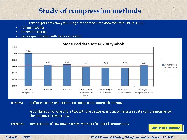 Study of compression methods Three algorithms analyzed using a set of measured data from the TPC in ALICE: • Huffman coding • Arithmetic coding • Vector quantization with delta calculation Results: Huffman coding and arithmetic coding alone approach entropy. A combination of one of the two with the vector quantization results in data compression below the entropy to almost 50%. Outlook: P. Aspell Investigation of low power design methods for digital components. CERN Christian Patauner EUDET Annual Meeting, Nikhef, Amsterdam, October 6 -8 2008
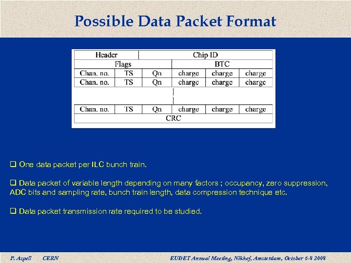 Possible Data Packet Format q One data packet per ILC bunch train. q Data packet of variable length depending on many factors ; occupancy, zero suppression, ADC bits and sampling rate, bunch train length, data compression technique etc. q Data packet transmission rate required to be studied. P. Aspell CERN EUDET Annual Meeting, Nikhef, Amsterdam, October 6 -8 2008
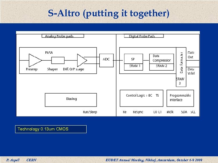 S-Altro (putting it together) Technology 0. 13 um CMOS P. Aspell CERN EUDET Annual Meeting, Nikhef, Amsterdam, October 6 -8 2008
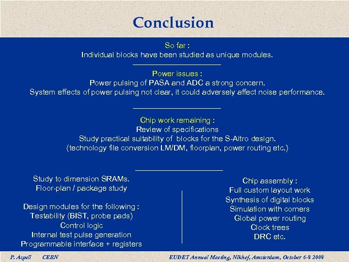 Conclusion So far : Individual blocks have been studied as unique modules. Power issues : Power pulsing of PASA and ADC a strong concern. System effects of power pulsing not clear, it could adversely affect noise performance. Chip work remaining : Review of specifications Study practical suitability of blocks for the S-Altro design. (technology file conversion LM/DM, floorplan, power routing etc. ) Study to dimension SRAMs. Floor-plan / package study Design modules for the following : Testability (BIST, probe pads) Control logic Internal test pulse generation Programmable interface + registers P. Aspell CERN Chip assembly : Full custom layout work Synthesis of digital blocks Simulation with corners Global power routing Clock trees DRC etc. EUDET Annual Meeting, Nikhef, Amsterdam, October 6 -8 2008


