43cfa5fe4c9fc6cb5fd37ee4fdafec72.ppt
- Количество слайдов: 51
 The Roadmap for Design and Design for Manufacturing Andrew B. Kahng, UC San Diego CSE & ECE Departments Chair, ITRS Design ITWG, 2001– 2003 ISMT Yield Council, September 25, 2003 A. Kahng, ISMT Yield Council, 030925
 Outline • The Design Roadmap • DFM: Symptoms, Problem, Solution • DFM Futures: Some Examples A. Kahng, ISMT Yield Council, 030925
 Design ITWG Contributions to ITRS • System Drivers Chapter – Defines IC products that drive manufacturing and design technologies – ORTCs + System Drivers = framework for technology requirements – Four System Driver classes • • SOC (Low-Power, High-Performance, Mixed-Technology) MPU Mixed-Signal Embedded Memory • Design Chapter – Design cost and productivity models – Five technology areas: design process / design system architecture, system-level design, logical/physical/circuit design, design verification, design test – Cross-cutting challenges: productivity, power, manufacturing integration, interference, error-tolerance • ORTC support – Frequency, Power, Density models A. Kahng, ISMT Yield Council, 030925
 Big Picture • Message: Cost of Design threatens continuation of the semiconductor roadmap – Design cost model – Challenges are now Crises • Strengthen bridge from semiconductors to applications, software, architectures – Hertz and bits are not the same as efficiency and utility – System Drivers chapter, with productivity and power foci • Strengthen bridges among ITRS technologies – “Shared bricks” can be solved (or, worked-around) more cost-effectively – “Manufacturing Integration” cross-cutting challenge – “Living ITRS” framework to promote consistency validation A. Kahng, ISMT Yield Council, 030925
 “Design-Manufacturing Integration” • ITRS Design Chapter: “Manufacturing Integration” = one of five Cross-Cutting Challenges • Goal: share red bricks with other ITRS technologies – Lithography CD variability requirement new Design techniques that can better handle variability – Mask data volume requirement solved by Design-Mfg interfaces and flows that pass functional requirements, verification knowledge to mask writing and inspection – ATE cost and speed red bricks solved by DFT, BIST/BOST techniques for high-speed I/O, signal integrity, analog/MS – Does “X initiative” have as much impact as copper? A. Kahng, ISMT Yield Council, 030925
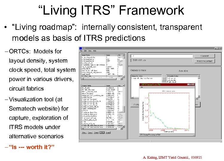 “Living ITRS” Framework • “Living roadmap”: internally consistent, transparent models as basis of ITRS predictions – ORTCs: Models for layout density, system clock speed, total system power in various drivers, circuit fabrics – Visualization tool (at Sematech website) for capture, exploration of ITRS models under alternative scenarios – “Is --- worth it? ” A. Kahng, ISMT Yield Council, 030925
 System Drivers Chapter • Defines the IC products that drive manufacturing and design technologies • Goal: ORTCs + System Drivers = “consistent framework for technology requirements” • Starts with macro picture – Market drivers – Convergence to SOC • Main content: System Drivers – – SOC – focus on low-power “PDA” (and, high-speed I/O) MPU – traditional processor core AM/S – four basic circuits and Figures of Merit Embedded Memory – e. DRAM, e. SRAM, e. NVM (flash) A. Kahng, ISMT Yield Council, 030925
 MPU Driver • Two MPU flavors – Cost-performance (“mobile”): constant 140 mm 2 die – High-performance (“server/desktop”): constant 310 mm 2 die • Stake in ground #1: MPU organization: multiple cores, on-board L 3 cache • More dedicated, less general-purpose logic • More cores help power management (lower frequency, lower Vdd, more parallelism overall power savings) • Reuse of cores helps design productivity • Redundancy helps yield and fault-tolerance • MPU and SOC converge (organization and design methodology) • Stake in ground #2: No more doubling of clock frequency at each node A. Kahng, ISMT Yield Council, 030925
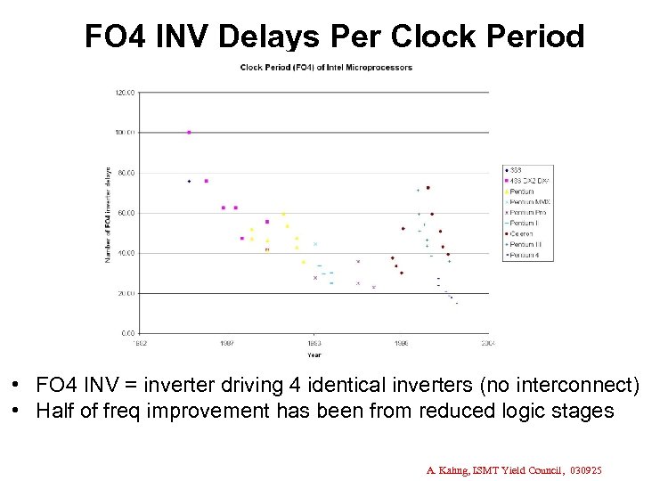 FO 4 INV Delays Per Clock Period • FO 4 INV = inverter driving 4 identical inverters (no interconnect) • Half of freq improvement has been from reduced logic stages A. Kahng, ISMT Yield Council, 030925
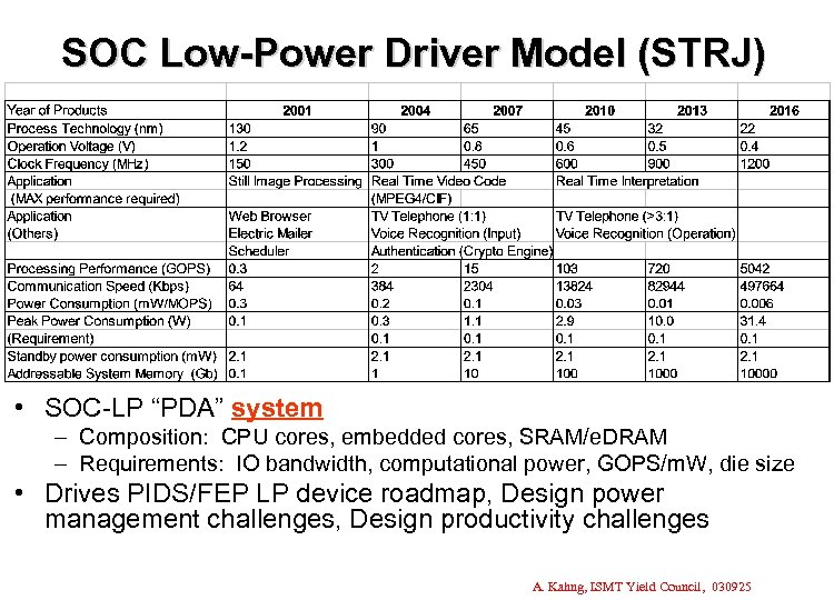 SOC Low-Power Driver Model (STRJ) • SOC-LP “PDA” system – Composition: CPU cores, embedded cores, SRAM/e. DRAM – Requirements: IO bandwidth, computational power, GOPS/m. W, die size • Drives PIDS/FEP LP device roadmap, Design power management challenges, Design productivity challenges A. Kahng, ISMT Yield Council, 030925
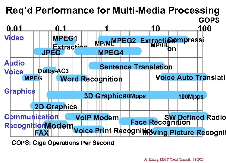 Req’d Performance for Multi-Media Processing 0. 01 0. 1 Video 1 10 GOPS 100 MPEG 1 Compressi MPEG 2 Extraction MP/ML MP/HL Extraction on MPEG 4 JPEG Audio Voice Dolby-AC 3 MPEG Word Graphics Sentence Translation Voice Auto Translatio Recognition 10 Mpps 3 D Graphics 100 Mpps 2 D Graphics Communication SW Defined Radio Vo. IP Modem Face Recognition Modem Voice Print Recognition Moving Picture Recognit FAX GOPS: Giga Operations Per Second A. Kahng, ISMT Yield Council, 030925
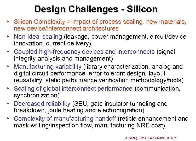 Design Challenges - Silicon • Silicon Complexity = impact of process scaling, new materials, new device/interconnect architectures • Non-ideal scaling (leakage, power management, circuit/device innovation, current delivery) • Coupled high-frequency devices and interconnects (signal integrity analysis and management) • Manufacturing variability (library characterization, analog and digital circuit performance, error-tolerant design, layout reusability, static performance verification methodology/tools) • Scaling of global interconnect performance (communication, synchronization) • Decreased reliability (SEU, gate insulator tunneling and breakdown, joule heating and electromigration) • Complexity of manufacturing handoff (reticle enhancement and mask writing/inspection flow, manufacturing NRE cost) A. Kahng, ISMT Yield Council, 030925
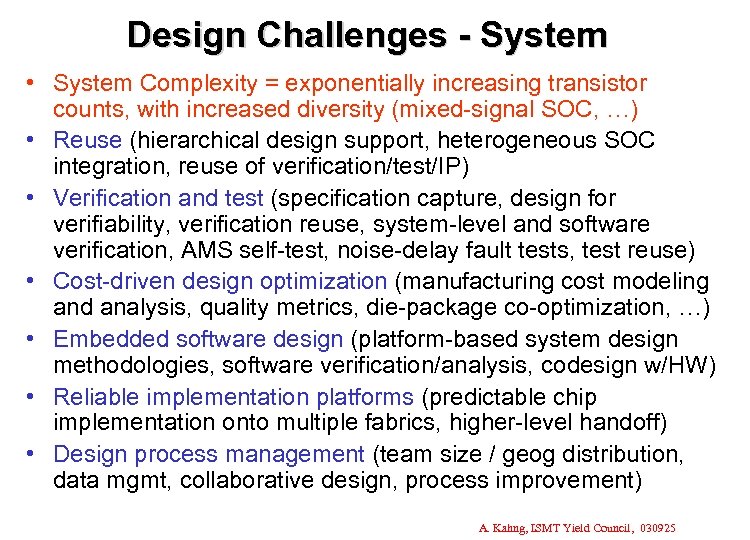 Design Challenges - System • System Complexity = exponentially increasing transistor counts, with increased diversity (mixed-signal SOC, …) • Reuse (hierarchical design support, heterogeneous SOC integration, reuse of verification/test/IP) • Verification and test (specification capture, design for verifiability, verification reuse, system-level and software verification, AMS self-test, noise-delay fault tests, test reuse) • Cost-driven design optimization (manufacturing cost modeling and analysis, quality metrics, die-package co-optimization, …) • Embedded software design (platform-based system design methodologies, software verification/analysis, codesign w/HW) • Reliable implementation platforms (predictable chip implementation onto multiple fabrics, higher-level handoff) • Design process management (team size / geog distribution, data mgmt, collaborative design, process improvement) A. Kahng, ISMT Yield Council, 030925
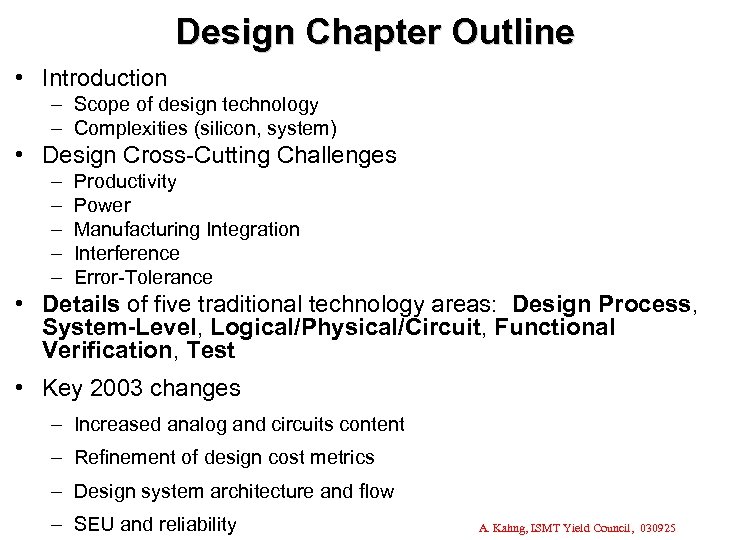 Design Chapter Outline • Introduction – Scope of design technology – Complexities (silicon, system) • Design Cross-Cutting Challenges – – – Productivity Power Manufacturing Integration Interference Error-Tolerance • Details of five traditional technology areas: Design Process, System-Level, Logical/Physical/Circuit, Functional Verification, Test • Key 2003 changes – Increased analog and circuits content – Refinement of design cost metrics – Design system architecture and flow – SEU and reliability A. Kahng, ISMT Yield Council, 030925
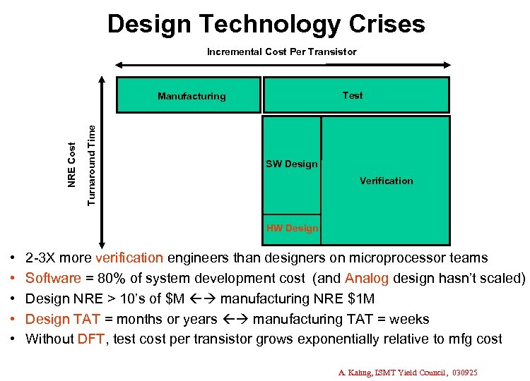 Design Technology Crises Incremental Cost Per Transistor Test Turnaround Time NRE Cost Manufacturing SW Design Verification HW Design • • • 2 -3 X more verification engineers than designers on microprocessor teams Software = 80% of system development cost (and Analog design hasn’t scaled) Design NRE > 10’s of $M manufacturing NRE $1 M Design TAT = months or years manufacturing TAT = weeks Without DFT, test cost per transistor grows exponentially relative to mfg cost A. Kahng, ISMT Yield Council, 030925
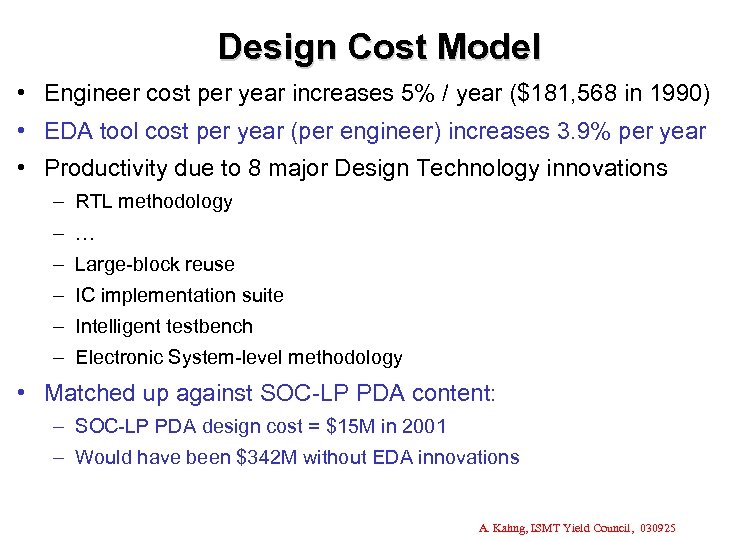 Design Cost Model • Engineer cost per year increases 5% / year ($181, 568 in 1990) • EDA tool cost per year (per engineer) increases 3. 9% per year • Productivity due to 8 major Design Technology innovations – RTL methodology – … – Large-block reuse – IC implementation suite – Intelligent testbench – Electronic System-level methodology • Matched up against SOC-LP PDA content: – SOC-LP PDA design cost = $15 M in 2001 – Would have been $342 M without EDA innovations A. Kahng, ISMT Yield Council, 030925
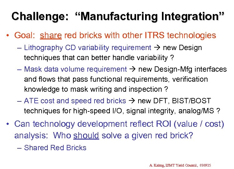 Challenge: “Manufacturing Integration” • Goal: share red bricks with other ITRS technologies – Lithography CD variability requirement new Design techniques that can better handle variability ? – Mask data volume requirement new Design-Mfg interfaces and flows that pass functional requirements, verification knowledge to mask writing and inspection ? – ATE cost and speed red bricks new DFT, BIST/BOST techniques for high-speed I/O, signal integrity, analog/MS ? • Can technology development reflect ROI (value / cost) analysis: Who should solve a given red brick? – Shared Red Bricks A. Kahng, ISMT Yield Council, 030925
 Example: Manufacturing Test • High-speed interfaces (networking, memory I/O) – Frequencies on same scale as overall tester timing accuracy • Heterogeneous SOC design – Test reuse – Integration of distinct test technologies within single device – Analog/mixed-signal test • Reliability screens failing – Burn-in screening not practical with lower Vdd, higher power budgets overkill impact on yield • Design Challenges: DFT, BIST – – Analog/mixed-signal Signal integrity and advanced fault models BIST for single-event upsets (in logic as well as memory) Reliability-related fault tolerance A. Kahng, ISMT Yield Council, 030925
 Example: Lithography • 10% CD uniformity requirement causes red bricks • 10% < 1 atomic monolayer at end of ITRS • This year: Lithography, PIDS, FEP agreed to relax CD uniformity requirement (but we still see red bricks) • Design challenge: Design for variability – Novel circuit topologies – Circuit optimization (conflict between slack minimization and guardbanding of quadratically increasing delay sensitivity) – Centering and design for $/wafer • Design challenge: Design for when devices, interconnects no longer 100% guaranteed correct – Can this save $$$ in manufacturing, verification, test costs? A. Kahng, ISMT Yield Council, 030925
 Outline • The Design Roadmap • DFM: Symptoms, Problem, Solution • DFM Futures: Some Examples A. Kahng, ISMT Yield Council, 030925
 Symptoms: Routing Rules (1) • Minimum area rules and via stacking – Stacking vias through multiple layers can cause minimum area violations (alignment tolerances, etc. ) – Via cells can be created that have more metal than minimum via overlap (used for intermediate layers in stacked vias) • Multiple-cut vias – Use multiple-cut vias cells to increase yield and reliability • Can be required for wires of certain widths – Multiple via cut patterns have different spacing rules • Four cuts in quadrilateral; five cuts in cross; six cuts in 2 x 3 array; … • With wide-wire spacing rules, complicates pin access – Cut-to-cut spacing rules check both cut-to-cut and metal-tometal when considering via-to-via spacing • Line-end extensions – Vias or line ends need additional metal overlap (0 th-order OPC) A. Kahng, ISMT Yield Council, 030925
 Symptoms: Routing Rules (2) • Width- and Length-dependent spacing rules – Width-dependent rules: domino effects – Variant: “parallel-run rule” (longer parallel runs more spacing) – Measuring length and width: halo rules affect computation • Influence rules or stub rules – A fat wire, e. g. , power/ground net, will influence the spacing rule within its surroundings any wire that is X um away from the fat wire needs to be at least Y um away from any other geometry. – Example: fat wire with thin tributaries • bigger spacing around every wire within certain distance of the thin tributaries • ECO insertion of a tributary causes complications • Strange jogs and spreading when wires enter an influenced area A. Kahng, ISMT Yield Council, 030925
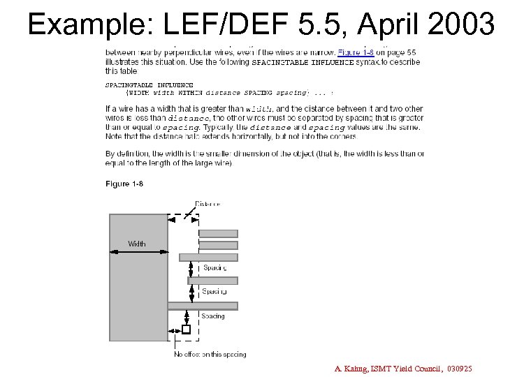 Example: LEF/DEF 5. 5, April 2003 A. Kahng, ISMT Yield Council, 030925
 Symptoms: Routing Rules (3) • Density – Grounded metal fills (dummy fill*) – Via isodensity rules and via farm rules (via layers must be filled and slotted, have width-dependent spacing rule analogs, etc. ) • Non-rectilinear ( -geometry) routing – X-Architecture: http: //www. xinitiative. org/ • Y-Architecture: http: //vlsicad. ucsd. edu/Yarchitecture/ , LSI Logic patents – Landing pad shapes (isothetic rectangle vs. octagon vs. circle), different spacings (~1. 1 x) between diagonal and Manhattan wires, etc. • More exceptions – More non-default classes (timing, EM reliability, …) • Not just power and clock – >0. 25 um width may be “wide” many exceptions A. Kahng, ISMT Yield Council, 030925
 Symptoms: Routing Rules • Degrade completion rates, runtime efficiency • “Postprocessing” likely no longer suffices – E. g. , antennas • There is no chip until the router is done • Must / Should / Can tomorrow’s IC routers “independently” address these issues? A. Kahng, ISMT Yield Council, 030925
 Whose Job Is It To Solve: • Mask NRE cost ( runtimes shapes complexity) • BEOL catastrophic yield loss – Deposited copper can infer yield loss mechanisms • Open faults more prevalent than short or bridging faults • High-resistance via faults • Cf. “non-tree routing” for reliability and yield? – Variability budget for planarization • Copper is soft dual-material polish mechanisms • Oxide erosion and copper dishing cross-sectional variability, inter-layer bridging faults, … • Low-k: thermal properties, anisotropy, nonuniformity • Resistivity at small conductor dimensions A. Kahng, ISMT Yield Council, 030925
 The Problem: Evolution • Conflicting goals – Designer: “freedom”, “reuse”, “migration” – EDA: “maintenance mode” – Process/foundry: “enhance perceived value” (= add rules) – Prisoner’s Dilemma: who will invest in change? • Fiddling: Incremental, linear extrapolation of current trajectory – “GDS-3” – Thin post-processing layers (decompaction, RET insertion, …) – Leads to “dark future” (12 th Japan DA Show keynote) A. Kahng, ISMT Yield Council, 030925
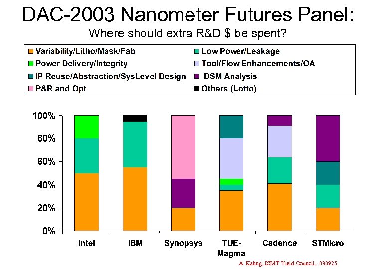 DAC-2003 Nanometer Futures Panel: Where should extra R&D $ be spent? A. Kahng, ISMT Yield Council, 030925
 The Solution: Co-Evolution • Designer, EDA, and process communities cooperate and co-evolve to maintain the cost (value) trajectory of Moore’s Law – Must escape Prisoner’s Dilemma – Must be financially viable – At 90 nm to 65 nm transition, this is a matter of survival for the worldwide semiconductor industry • Example Focus Areas: – – – Explicit manufacturability and cost/value optimization Restricted layout Intelligent mask data prep “Analog” (not binary) rules (Many layout and design optimizations) Disclaimer: Not a complete listing A. Kahng, ISMT Yield Council, 030925
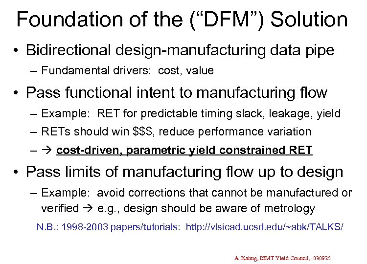 Foundation of the (“DFM”) Solution • Bidirectional design-manufacturing data pipe – Fundamental drivers: cost, value • Pass functional intent to manufacturing flow – Example: RET for predictable timing slack, leakage, yield – RETs should win $$$, reduce performance variation – cost-driven, parametric yield constrained RET • Pass limits of manufacturing flow up to design – Example: avoid corrections that cannot be manufactured or verified e. g. , design should be aware of metrology N. B. : 1998 -2003 papers/tutorials: http: //vlsicad. ucsd. edu/~abk/TALKS/ A. Kahng, ISMT Yield Council, 030925
 Outline • The Design Roadmap • DFM: Symptoms, Problem, Solution • DFM Futures: Some Examples A. Kahng, ISMT Yield Council, 030925
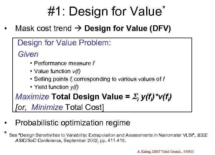 #1: Design for Value* • Mask cost trend Design for Value (DFV) Design for Value Problem: Given • • Performance measure f Value function v(f) Selling points fi corresponding to various values of f Yield function y(f) Maximize Total Design Value = i y(fi)*v(fi) [or, Minimize Total Cost] • Probabilistic optimization regime * See "Design Sensitivities to Variability: Extrapolation and Assessments in Nanometer VLSI", IEEE ASIC/So. C Conference, September 2002, pp. 411 -415. A. Kahng, ISMT Yield Council, 030925
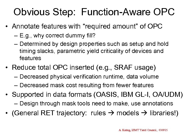 Obvious Step: Function-Aware OPC • Annotate features with “required amount” of OPC – E. g. , why correct dummy fill? – Determined by design properties such as setup and hold timing slacks, parametric yield criticality of devices and features • Reduce total OPC inserted (e. g. , SRAF usage) – Decreased physical verification runtime, data volume – Decreased mask cost resulting from fewer features • Supported in data formats (OASIS, IBM GL-I, OA/UDM) – Design through mask tools need to make, use annotations • (General RET trajectory: rules models libraries!) A. Kahng, ISMT Yield Council, 030925
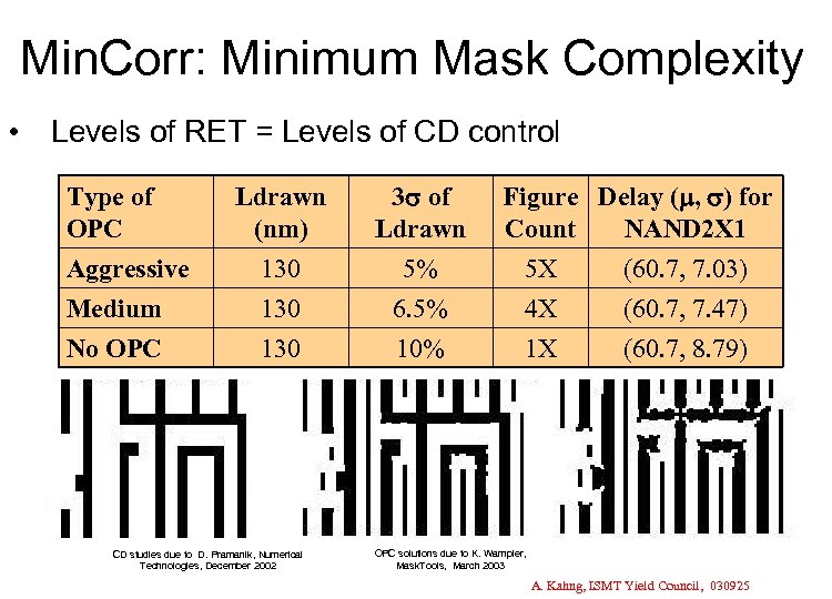 Min. Corr: Minimum Mask Complexity • Levels of RET = Levels of CD control • Levels of RET = Type of Ldrawn 3 of OPC levels of CD(nm) control Ldrawn Figure Delay ( , ) for Count NAND 2 X 1 Aggressive 130 5% 5 X (60. 7, 7. 03) Medium No OPC 130 6. 5% 10% 4 X 1 X (60. 7, 7. 47) (60. 7, 8. 79) CD studies due to D. Pramanik, Numerical Technologies, December 2002 OPC solutions due to K. Wampler, Mask. Tools, March 2003 A. Kahng, ISMT Yield Council, 030925
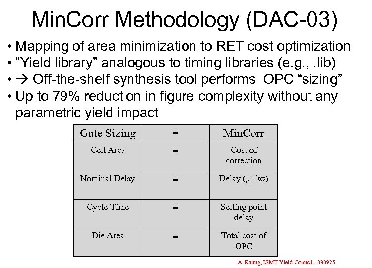 Min. Corr Methodology (DAC-03) • Mapping of area minimization to RET cost optimization • “Yield library” analogous to timing libraries (e. g. , . lib) • Off-the-shelf synthesis tool performs OPC “sizing” • Up to 79% reduction in figure complexity without any parametric yield impact Gate Sizing Min. Corr Cell Area Cost of correction Nominal Delay ( +k ) Cycle Time Selling point delay Die Area Total cost of OPC A. Kahng, ISMT Yield Council, 030925
 #2: Process-Aware Design • Anisotropy in H vs. V bias – Features in one direction (scanning, raster write, …) may be better controllable than those in the orthogonal direction – Single orientation throughout layout is preferred – Dominant (critical-feature) orientation in layout design should match write direction • Wafer symmetries (e. g. , etch gradient due to spin-on) • Iso-Dense balancing (imaging through focus) A. Kahng, ISMT Yield Council, 030925
 #3: Intelligent MDP+Write • MDP driven by (write error * MEEF) = wafer CD error – Partitioning into multiple gray-scale writing passes – Apertures, beam currents, dwell times, shot ordering, … • EDA tools define stripe, major field, subfield boundaries! • Electrical / functional defect criteria A. Kahng, ISMT Yield Council, 030925
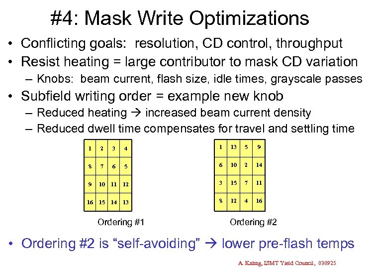 #4: Mask Write Optimizations • Conflicting goals: resolution, CD control, throughput • Resist heating = large contributor to mask CD variation – Knobs: beam current, flash size, idle times, grayscale passes • Subfield writing order = example new knob – Reduced heating increased beam current density – Reduced dwell time compensates for travel and settling time 1 2 3 4 1 13 5 9 8 7 6 5 6 10 2 14 9 10 11 12 3 15 7 11 16 15 14 13 8 12 4 16 Ordering #1 Ordering #2 • Ordering #2 is “self-avoiding” lower pre-flash temps A. Kahng, ISMT Yield Council, 030925
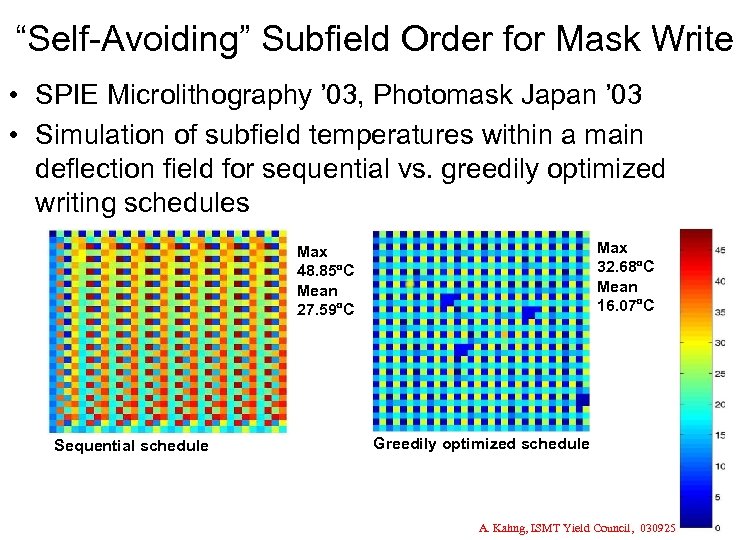 “Self-Avoiding” Subfield Order for Mask Write • SPIE Microlithography ’ 03, Photomask Japan ’ 03 • Simulation of subfield temperatures within a main deflection field for sequential vs. greedily optimized writing schedules Max 32. 68 C Mean 16. 07 C Max 48. 85 C Mean 27. 59 C Sequential schedule Greedily optimized schedule A. Kahng, ISMT Yield Council, 030925
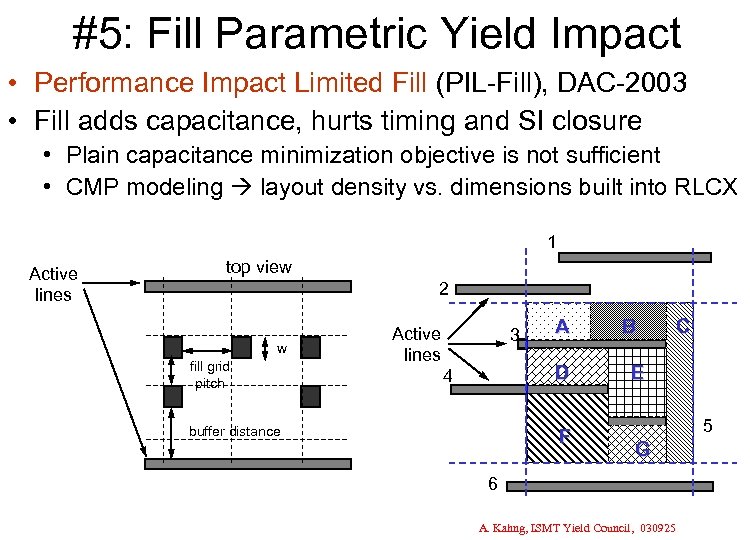 #5: Fill Parametric Yield Impact • Performance Impact Limited Fill (PIL-Fill), DAC-2003 • Fill adds capacitance, hurts timing and SI closure • Plain capacitance minimization objective is not sufficient • CMP modeling layout density vs. dimensions built into RLCX 1 Active lines top view 2 w fill grid pitch Active lines 3 A D 4 buffer distance F B C E 5 G 6 A. Kahng, ISMT Yield Council, 030925
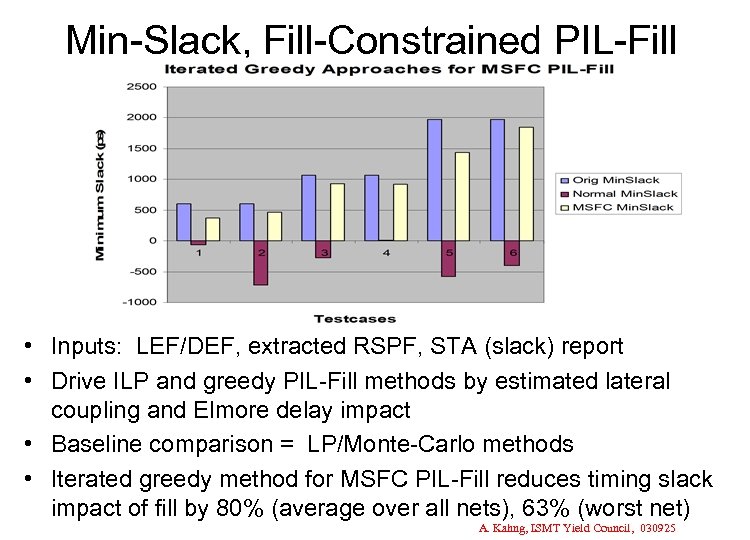 Min-Slack, Fill-Constrained PIL-Fill • Inputs: LEF/DEF, extracted RSPF, STA (slack) report • Drive ILP and greedy PIL-Fill methods by estimated lateral coupling and Elmore delay impact • Baseline comparison = LP/Monte-Carlo methods • Iterated greedy method for MSFC PIL-Fill reduces timing slack impact of fill by 80% (average over all nets), 63% (worst net) A. Kahng, ISMT Yield Council, 030925
 #6: Analog Rules • We don’t need no $#(*&(! “rules” – Rules just make lithographers feel better (? ) • Ultimately, bottom line is cost of ownership, TCOG • Given adequate models of MDP, RET and Litho flows, design tools can and should optimize parametric yield, $/wafer, profits – More examples: critical-area reduction by decompaction, introducing redundancy (vias, wires), … • Automated learning of models and “implicit rules” – Current approach: test wafers, test structures, second-hand understanding – Future: machine learning techniques A. Kahng, ISMT Yield Council, 030925
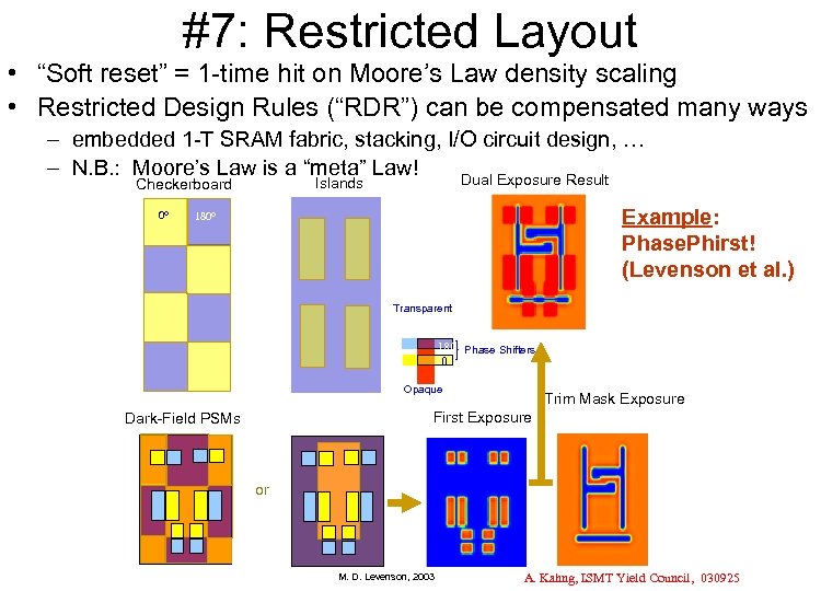 #7: Restricted Layout • “Soft reset” = 1 -time hit on Moore’s Law density scaling • Restricted Design Rules (“RDR”) can be compensated many ways – embedded 1 -T SRAM fabric, stacking, I/O circuit design, … – N. B. : Moore’s Law is a “meta” Law! Dual Exposure Result Islands Checkerboard 0 Example: Phase. Phirst! (Levenson et al. ) 180 Transparent 180 Phase Shifters 0 Opaque Trim Mask Exposure First Exposure Dark-Field PSMs or M. D. Levenson, 2003 A. Kahng, ISMT Yield Council, 030925
 #7: Charging and Antennas • Process steps use plasmas, charged particles – Electrical fields over gate oxides induce damage (Vt shift) or breakdown • Limit antenna ratio = (Apoly + AM 1 + …) / Agate-ox – AMx = metal(x) area that is electrically connected to node without using metal (x+1), and not connected to an active area – Bridging (break antenna by hopping to higher layer) • Extra wiring, vias, congestion – Reverse-biased diode or source-drain contact near gate • Leakage, area, timing penalties • Will antenna ratios continue to decrease? – High-k gate dielectrics increased physical Tox less leaky, hard failure modes? • More preemption (no post-processing, or dioded cells)? • Tradeoff unfixed antenna yield penalty for fixed antenna yield loss? A. Kahng, ISMT Yield Council, 030925
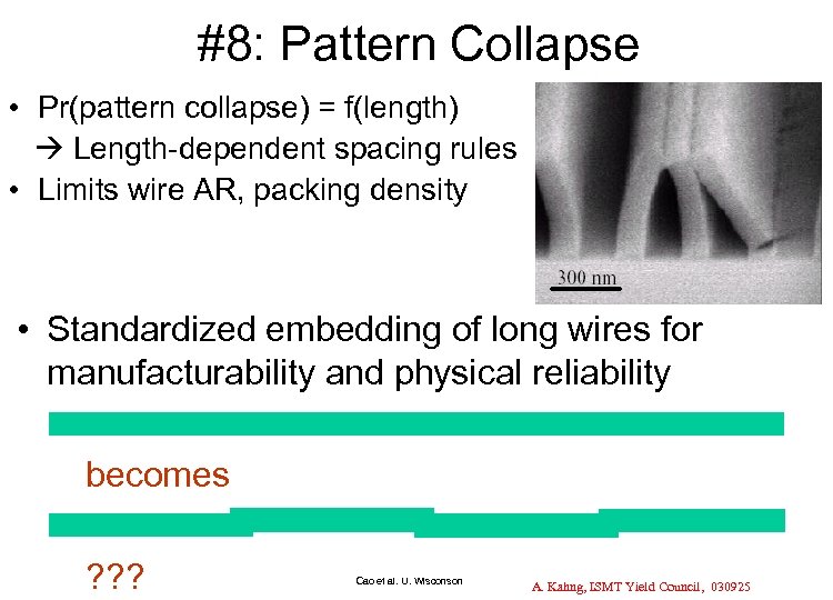 #8: Pattern Collapse • Pr(pattern collapse) = f(length) Length-dependent spacing rules • Limits wire AR, packing density • Standardized embedding of long wires for manufacturability and physical reliability becomes ? ? ? Cao et al. U. Wisconson A. Kahng, ISMT Yield Council, 030925
 #9: Data Compression • Today: RET + complexity exploding data volume • Partitioning of compression and decompression? – Equipment architecture question – where to put engines, I/F’s, storage? – Largely orthogonal to design considerations – Procedural compression largely unexplored? (Ex: Verilog + SP&R binaries + runscripts = representation of detail-routed layout) • Design for compressibility? (DATE ’ 03, SPIE ML ’ 03) – What is ROI of relaxing constraints on layout? Of +k bytes of data? – How context-sensitive must patterning be? (Lessons from RET…) • Use of lossy compression? (SPIE ML ’ 03) – What design features can be “lost”? (Ex: dummy fill) A. Kahng, ISMT Yield Council, 030925
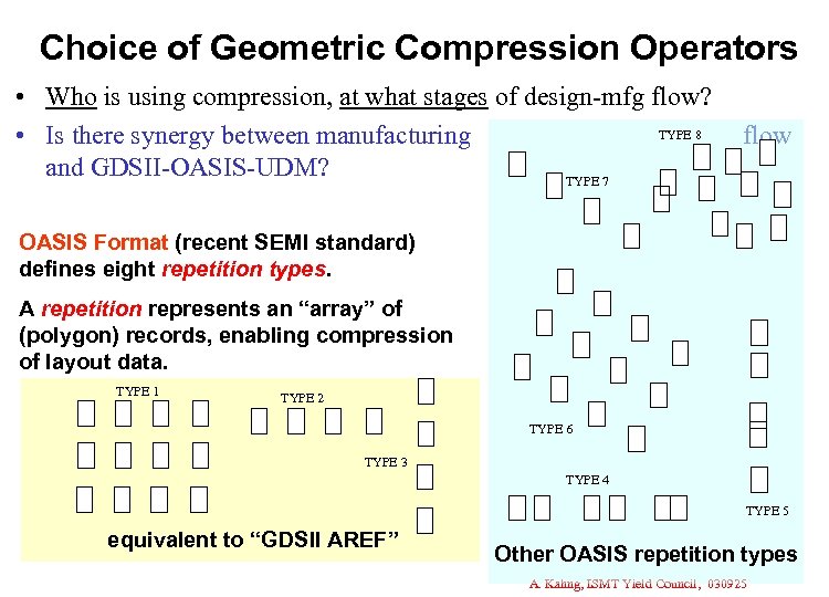 Choice of Geometric Compression Operators • Who is using compression, at what stages of design-mfg flow? TYPE 8 • Is there synergy between manufacturing and GDSII-OASIS-UDM? TYPE 7 flow OASIS Format (recent SEMI standard) defines eight repetition types. A repetition represents an “array” of (polygon) records, enabling compression of layout data. TYPE 1 TYPE 2 TYPE 6 TYPE 3 TYPE 4 TYPE 5 equivalent to “GDSII AREF” Other OASIS repetition types A. Kahng, ISMT Yield Council, 030925
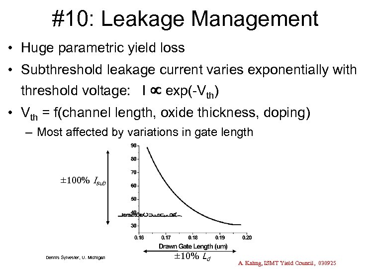 #10: Leakage Management • Huge parametric yield loss • Subthreshold leakage current varies exponentially with threshold voltage: I exp(-Vth) • Vth = f(channel length, oxide thickness, doping) – Most affected by variations in gate length ± 100% Isub Dennis Sylvester, U. Michigan ± 10% Ld A. Kahng, ISMT Yield Council, 030925
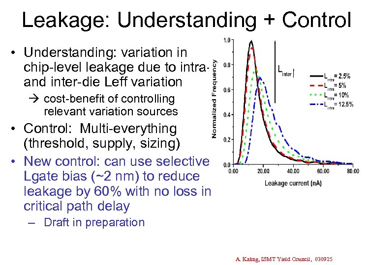 Leakage: Understanding + Control • Understanding: variation in chip-level leakage due to intraand inter-die Leff variation cost-benefit of controlling relevant variation sources • Control: Multi-everything (threshold, supply, sizing) • New control: can use selective Lgate bias (~2 nm) to reduce leakage by 60% with no loss in critical path delay – Draft in preparation A. Kahng, ISMT Yield Council, 030925
 Conclusions • Designer, EDA, and mask communities must co-evolve to maintain the cost (value) trajectory of Moore’s Law – Wakeup call: Intel 157 nm announcement • Basic goal: bidirectional design-mfg data pipe – Drivers: cost, value – Pass functional intent to mask and foundry flows – Pass limits of mask and foundry flows up to design • Several examples given – – – Manufacturability and cost/value optimization Leakage power Restricted layout Intelligent mask data prep Analog rules • Please pay someone to do this! A. Kahng, ISMT Yield Council, 030925
 THANK YOU ! A. Kahng, ISMT Yield Council, 030925


