13dc2128ca52b19df9583b22e161c099.ppt
- Количество слайдов: 26
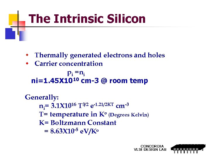 The Intrinsic Silicon • Thermally generated electrons and holes • Carrier concentration pi =ni ni=1. 45 X 1010 cm-3 @ room temp Generally: ni= 3. 1 X 10¹⁶ T 3/2 e-1. 21/2 KT cm-3 T= temperature in Ko (Degrees Kelvin) K= Boltzmann Constant = 8. 63 X 10 -5 e. V/Ko
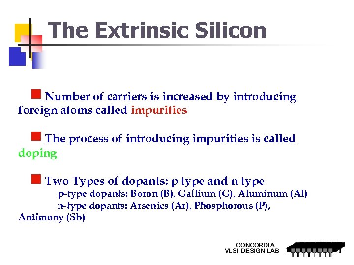 The Extrinsic Silicon Number of carriers is increased by introducing foreign atoms called impurities The process of introducing impurities is called doping Two Types of dopants: p type and n type p-type dopants: Boron (B), Gallium (G), Aluminum (Al) n-type dopants: Arsenics (Ar), Phosphorous (P), Antimony (Sb)
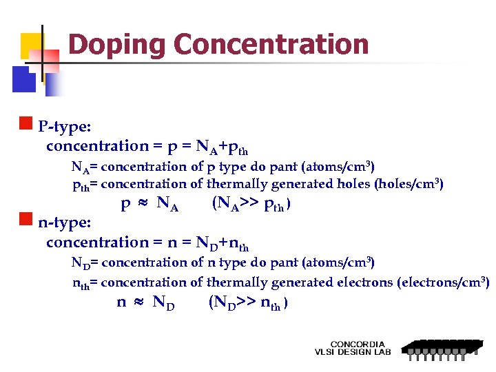 Doping Concentration P-type: concentration = p = NA+pth NA= concentration of p type do pant (atoms/cm 3) pth= concentration of thermally generated holes (holes/cm 3) p NA (NA>> pth ) n-type: concentration = ND+nth ND= concentration of n type do pant (atoms/cm 3) nth= concentration of thermally generated electrons (electrons/cm 3) n ND (ND>> nth )
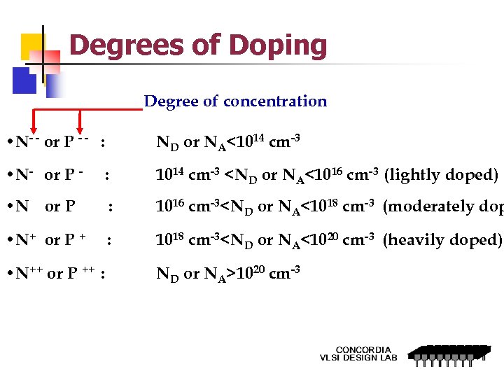 Degrees of Doping Degree of concentration • N- - or P - - : ND or NA<1014 cm-3 • N- or P - : 1014 cm-3
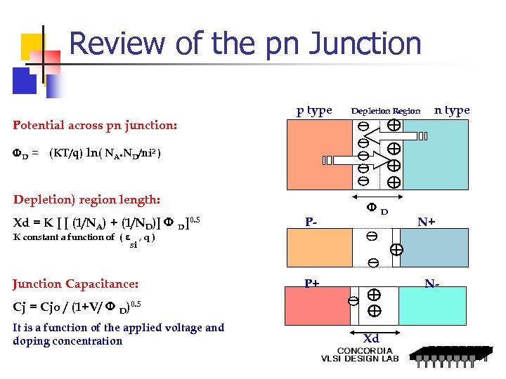 Review of the pn Junction p type Depletion Region n type Potential across pn junction: D = (KT/q) ln( NA. ND/ni 2 ) Depletion) region length: Xd = K [ [ (1/NA) + (1/ND)] K constant a function of ( ε , q ) si D ]0. 5 Junction Capacitance: P- P+ N+ N- Cj = Cjo / (1+V/ D)0. 5 It is a function of the applied voltage and doping concentration D Xd
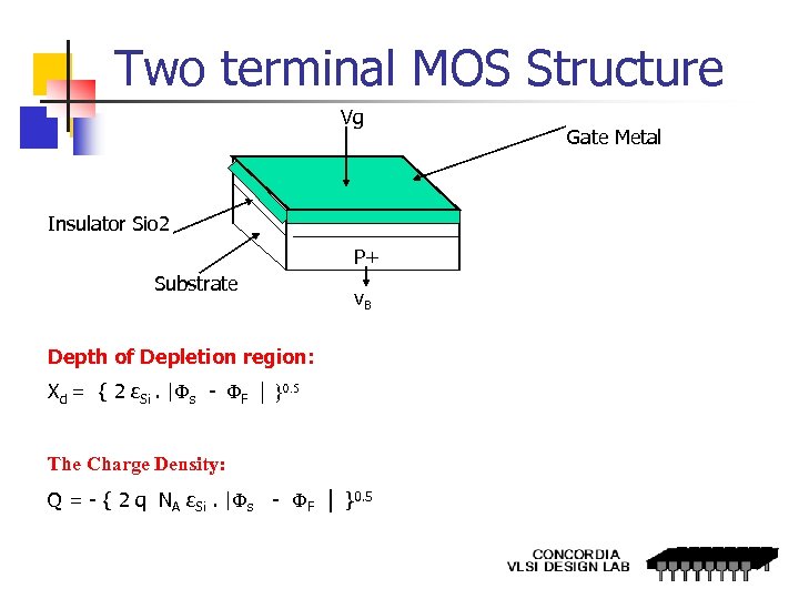 Two terminal MOS Structure Vg Insulator Sio 2 P+ Substrate v. B Depth of Depletion region: Xd = { 2 εSi. | s - F │ }0. 5 The Charge Density: Q = - { 2 q NA εSi. | s - F │ }0. 5 Gate Metal
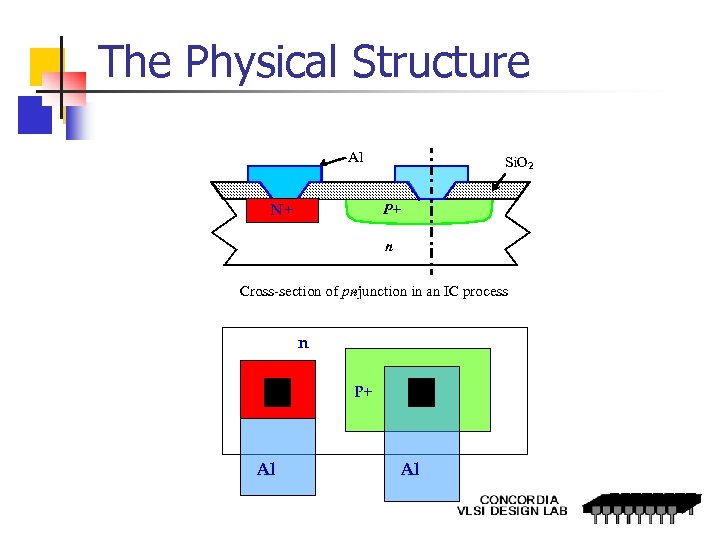 The Physical Structure Al N+ Si. O 2 P+ n Cross-section of pn -junction in an IC process n P+ Al Al
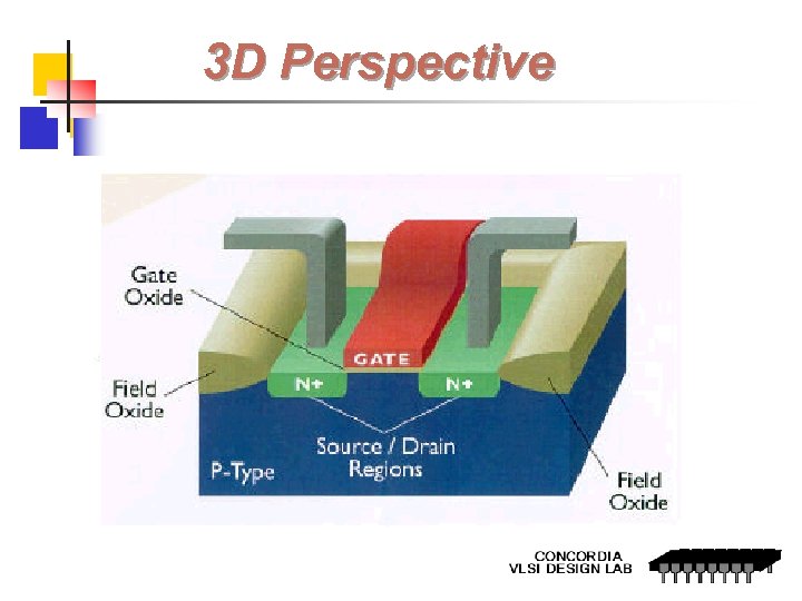 3 D Perspective
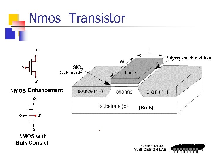 Nmos Transistor D Polycrystalline silicon G Gate oxide Gate S NMOS Enhancement D (Bulk) G B S NMOS with Bulk Contact
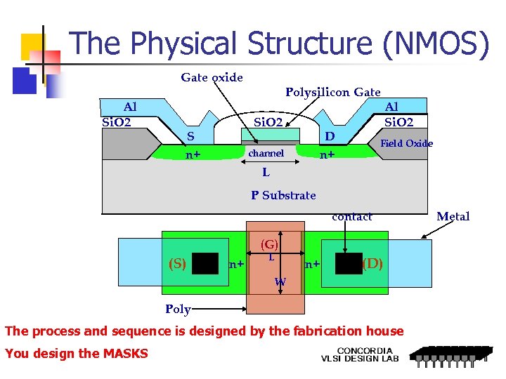 The Physical Structure (NMOS) Gate oxide Al Si. O 2 Field Oxide Polysilicon Gate Si. O 2 S n+ D n+ channel Al Si. O 2 Field Oxide L P Substrate contact (G) (S) n+ L n+ (D) W Poly The process and sequence is designed by the fabrication house You design the MASKS Metal
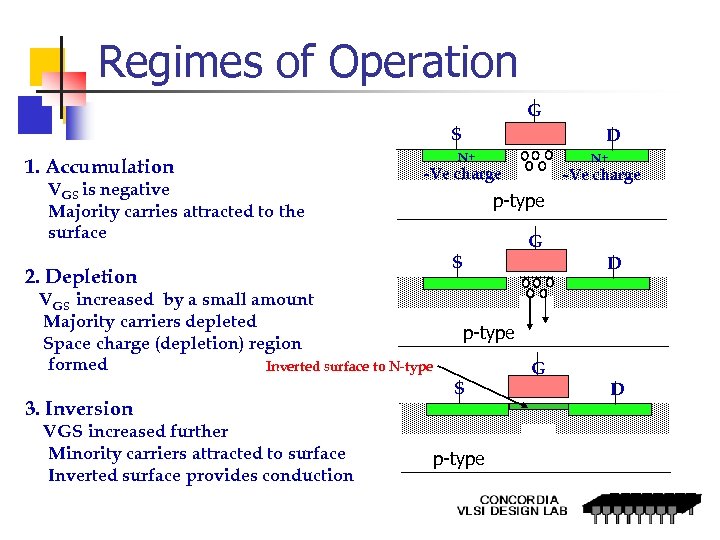 Regimes of Operation G S 1. Accumulation VGS is negative Majority carries attracted to the surface VGS increased by a small amount Majority carriers depleted Space charge (depletion) region formed Inverted surface to N-type VGS increased further Minority carriers attracted to surface Inverted surface provides conduction N+ N+ -Ve charge 2. Depletion 3. Inversion D -Ve charge p-type G S D p-type S p-type G D
 The Threshold Voltage §The voltage applied between the gate and the source which causes the beginning of the channel surface strong inversion. §Threshold voltage Vt is a function of : n n n Vfb = flatband voltage; depends on difference in work function between gate and substrate and on fixed surface charge. s = surface potential. Gate oxide thickness. Charge in the channel area. Additional ion implantation. n Typical values: 0. 2 V to 1. 0 V for NMOS and -0. 2 to -1. 0 V for PMOS
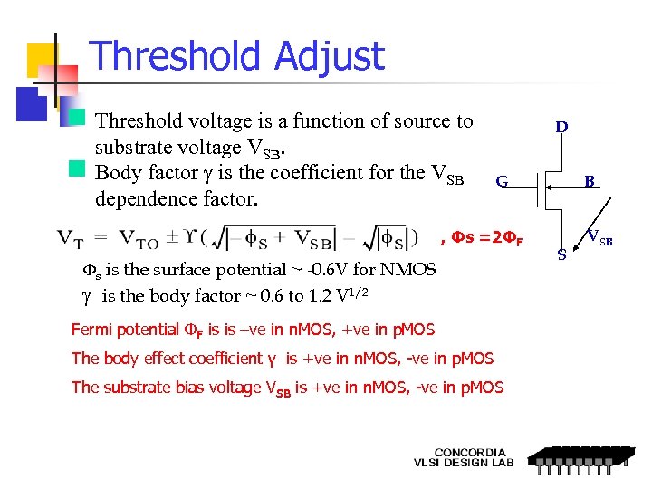 Threshold Adjust D G , Φs =2ΦF s is the surface potential ~ -0. 6 V for NMOS is the body factor ~ 0. 6 to 1. 2 V 1/2 Fermi potential ΦF is is –ve in n. MOS, +ve in p. MOS The body effect coefficient γ is +ve in n. MOS, -ve in p. MOS The substrate bias voltage VSB is +ve in n. MOS, -ve in p. MOS B S g Threshold voltage is a function of source to substrate voltage VSB. g Body factor is the coefficient for the VSB dependence factor. VSB
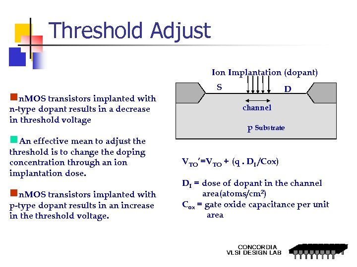 Threshold Adjust Ion Implantation (dopant) gn. MOS transistors implanted with n-type dopant results in a decrease in threshold voltage g. An effective mean to adjust the threshold is to change the doping concentration through an ion implantation dose. gn. MOS transistors implanted with p-type dopant results in an increase in the threshold voltage. S D channel p Substrate VTO’=VTO + (q. DI /Cox) DI = dose of dopant in the channel area(atoms/cm 2) Cox = gate oxide capacitance per unit area
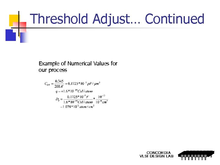 Threshold Adjust… Continued Example of Numerical Values for our process
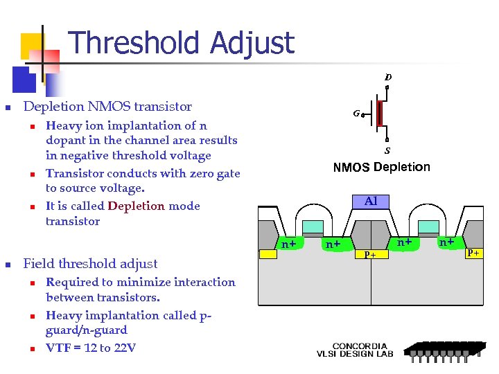 Threshold Adjust D n Depletion NMOS transistor n n n G Heavy ion implantation of n dopant in the channel area results in negative threshold voltage Transistor conducts with zero gate to source voltage. It is called Depletion mode transistor S NMOS Depletion Al n+ n Field threshold adjust n n n Required to minimize interaction between transistors. Heavy implantation called pguard/n-guard VTF = 12 to 22 V P+ n+ n+ P+
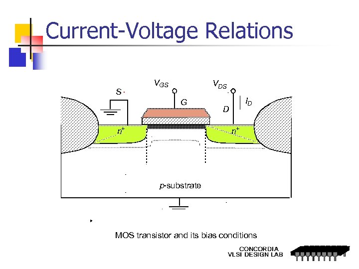 Current-Voltage Relations S VGS VDS G n+ ID D n+ p-substrate MOS transistor and its bias conditions
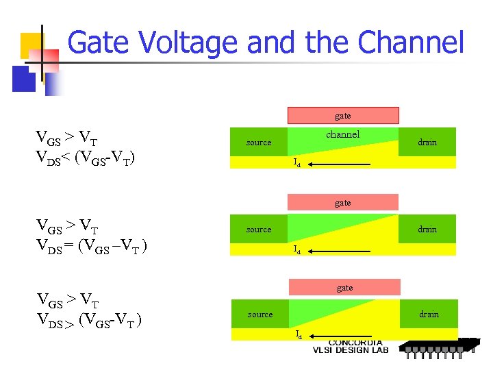 Gate Voltage and the Channel gate VGS > VT VDS< (VGS-VT) channel source drain Id gate VGS > VT VDS = (VGS –VT ) VGS > VT VDS > (VGS-VT ) source drain Id gate source drain Id
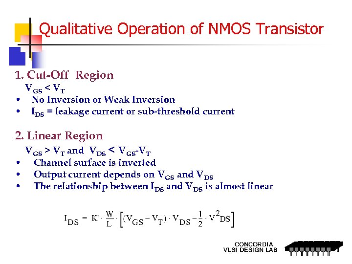 Qualitative Operation of NMOS Transistor 1. Cut-Off Region VGS < VT • No Inversion or Weak Inversion • IDS = leakage current or sub-threshold current 2. Linear Region VGS > VT and VDS < VGS-VT • Channel surface is inverted • Output current depends on VGS and VDS • The relationship between IDS and VDS is almost linear
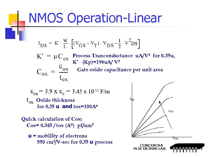 NMOS Operation-Linear Process Tranconductance u. A/V 2 for 0. 35 u, K’ (Kp)=196 u. A/ V 2 Gate oxide capacitance per unit area eox = 3. 9 x eo = 3. 45 x 10 -11 F/m tox Oxide thickness for 0. 35 u and tox=100 Ao Quick calculation of Cox: Cox= 0. 345 / tox (Ao) pf/um 2 u = mobility of electrons 550 cm 2/V-sec for 0. 35 u process
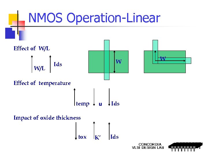 NMOS Operation-Linear Effect of W/L W Ids Effect of temperature temp u Ids K’ Ids Impact of oxide thickness tox W
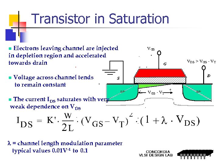 Transistor in Saturation Electrons leaving channel are injected in depletion region and accelerated towards drain VGS g g Voltage across channel tends to remain constant VDS > VGS - VT G D S n+ The current IDS saturates with very weak dependence on VDS g = channel length modulation parameter typical values 0. 01 V-1 to 0. 1 - VGS - VT + n+
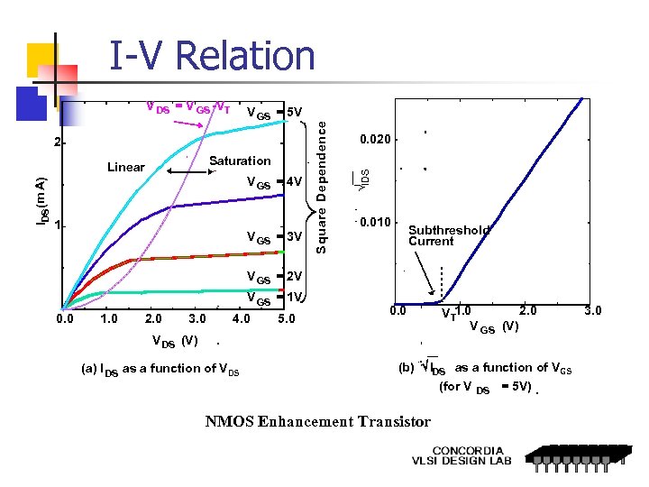 V GS = 5 V 2 Saturation IDS (m A) Linear V GS = 4 V 1 V GS = 3 V 0. 020 ÖIDS V DS = V GS -VT Square D ependence I-V Relation 0. 010 Subthreshold Current V GS = 2 V V GS = 1 V 0. 0 1. 0 2. 0 3. 0 4. 0 5. 0 0. 0 V DS (V) (a) I DS as a function of VDS 2. 0 VT 1. 0 V GS (V) (b) Ö IDS as a function of VGS (for V NMOS Enhancement Transistor DS = 5 V) . 3. 0
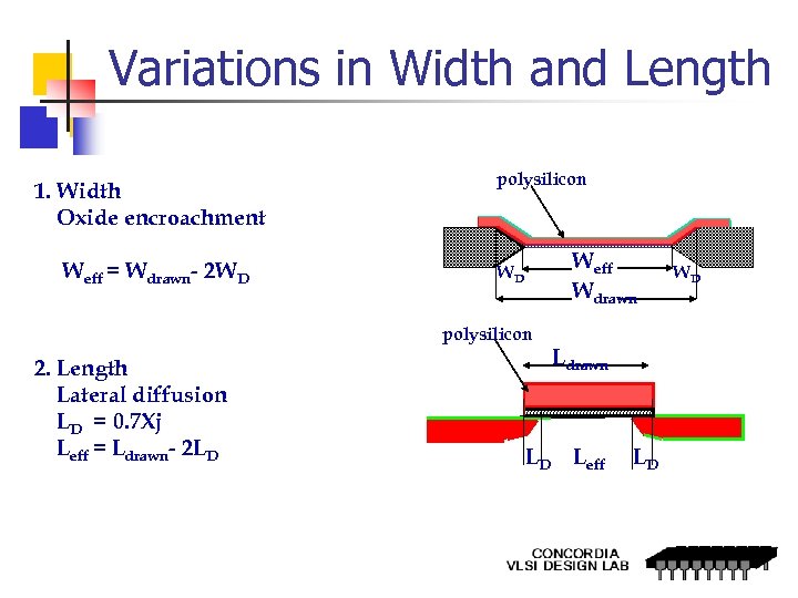 Variations in Width and Length 1. Width Oxide encroachment Weff = Wdrawn- 2 WD polysilicon Weff Wdrawn WD polysilicon 2. Length Lateral diffusion LD = 0. 7 Xj Leff = Ldrawn- 2 LD Ldrawn LD Leff LD WD
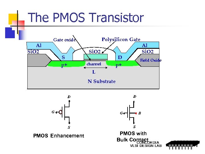 The PMOS Transistor Al Si. O 2 Polysilicon Gate oxide Si. O 2 S p+ Field Oxide channel D p+ Al Si. O 2 Field Oxide L N Substrate D D G G S PMOS Enhancement B S PMOS with Bulk Contact
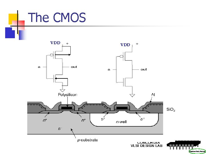 The CMOS VDD Prentice Hall/Rabaey


