bb89a8be52626900a7ea0038efd104df.ppt
- Количество слайдов: 145
 The Functions of a Computer Review 1
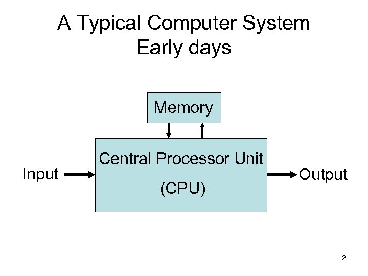 A Typical Computer System Early days Memory Input Central Processor Unit (CPU) Output 2
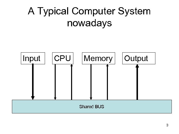 A Typical Computer System nowadays Input CPU Memory Output Shared BUS 3
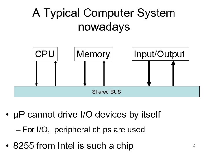 A Typical Computer System nowadays CPU Memory Input/Output Shared BUS • μP cannot drive I/O devices by itself – For I/O, peripheral chips are used • 8255 from Intel is such a chip 4
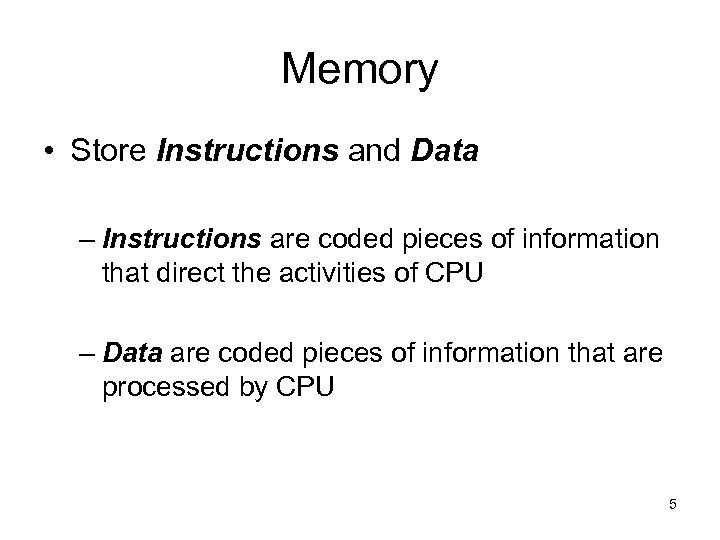 Memory • Store Instructions and Data – Instructions are coded pieces of information that direct the activities of CPU – Data are coded pieces of information that are processed by CPU 5
 Input Ports • But often the memory is not large enough to store the entire data required for a particular application • The problem can be resolved by providing the computer with one or more Input Ports • Also Input Ports enable Computer to receive information from external equipments 6
 Output Ports • Computers also require Output Ports – To communicate the results of its processing to the outside world • To display unit : for human operator • To a peripheral device to produce ‘hard copy’ : Printer • To a peripheral storage device : Hard Disk • Or the output may constitute process control signals that control the operations of another system : Process control in industry 7
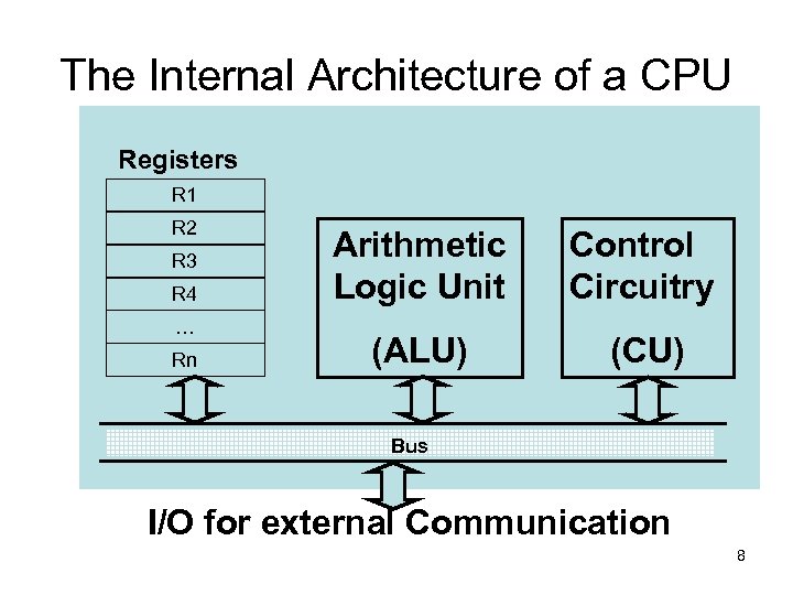 The Internal Architecture of a CPU Registers R 1 R 2 R 3 R 4 … Rn Arithmetic Logic Unit Control Circuitry (ALU) (CU) Bus I/O for external Communication 8
 Registers • Temporary storage unit within the CPU • Some registers have dedicated uses • Others are for more general purpose use • Often in some µP one register is specially known as Accumulator • Numbers of registers vary from µP to µP 9
 ALU • As its name implies, ALU is that portion of the CPU hardware which performs the arithmetic and logic operations on the binary data • Generally ALU contains simply an Adder – to perform all arithmetic operations like • Subtraction, multiplication, division – and all logic operations like • AND, OR, NOT 10
 ALU (cont…) • ALU also contains Flag Bits which specify certain conditions/status that arise after arithmetic and logic operations 11
 CU • CU is the primary functional unit within a CPU • CU maintains the proper sequence of events required for any processing task – Using clock inputs • CU issues the appropriate signals for initiating the proper processing action – To units both internal and external to CPU • Often CU is capable of responding to external 12 signals known as interrupt
 Interrupt • An Interrupt request will cause the CU to temporarily interrupt main program execution to serve the interrupting device • After serving the interrupting device, the CU will automatically return to the main program 13
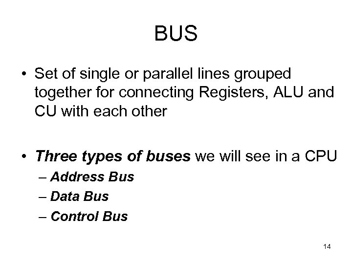 BUS • Set of single or parallel lines grouped together for connecting Registers, ALU and CU with each other • Three types of buses we will see in a CPU – Address Bus – Data Bus – Control Bus 14
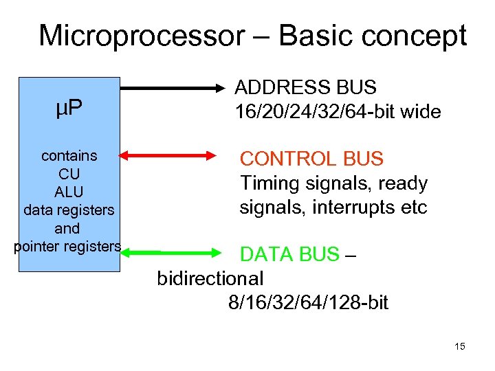 Microprocessor – Basic concept µP contains CU ALU data registers and pointer registers ADDRESS BUS 16/20/24/32/64 -bit wide CONTROL BUS Timing signals, ready signals, interrupts etc DATA BUS – bidirectional 8/16/32/64/128 -bit 15
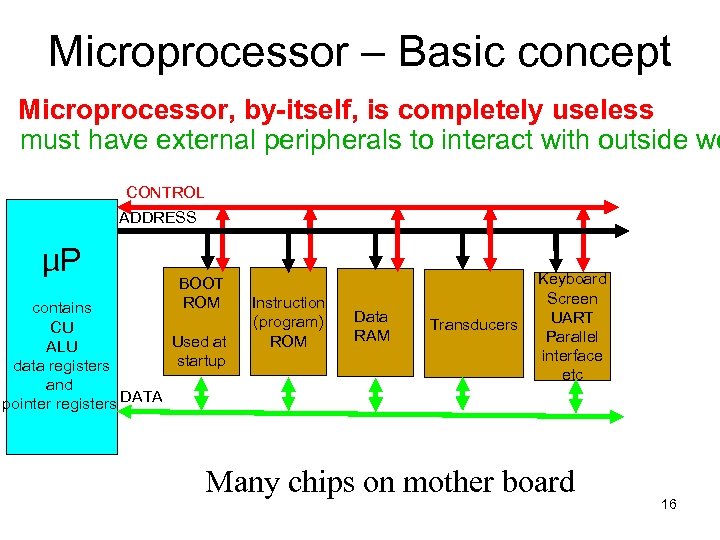 Microprocessor – Basic concept Microprocessor, by-itself, is completely useless must have external peripherals to interact with outside wo CONTROL ADDRESS µP BOOT ROM contains CU Used at ALU startup data registers and pointer registers DATA Instruction (program) ROM Data RAM Transducers Keyboard Screen UART Parallel interface etc Many chips on mother board 16
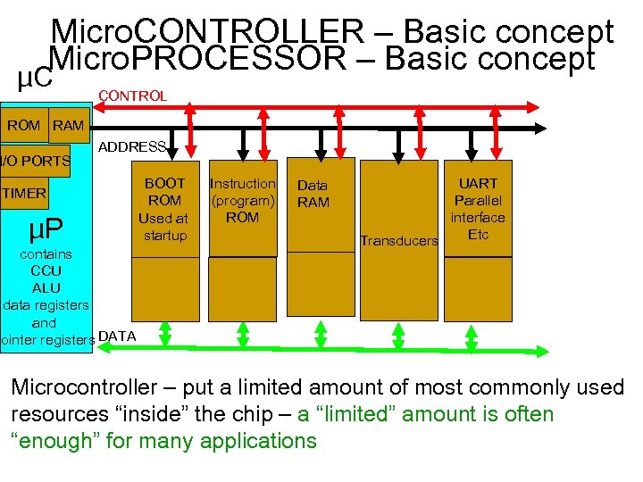 Micro. CONTROLLER – Basic concept Micro. PROCESSOR – Basic concept µC CONTROL ROM RAM I/O PORTS ADDRESS TIMER µP contains CCU ALU data registers and pointer registers DATA BOOT ROM Used at startup Instruction (program) ROM Data RAM UART Parallel interface Etc Transducers Microcontroller – put a limited amount of most commonly used resources “inside” the chip – a “limited” amount is often “enough” for many applications
 Advantages of micro. CONTROLLER over micro. PROCESSOR • Pin count down • Design time down, Board layout size down • Upgrade path easier – matching between peripherals for speed • Cost down – bulk purchases • Reliability up • Common software / hardware design environment available from manufacturer
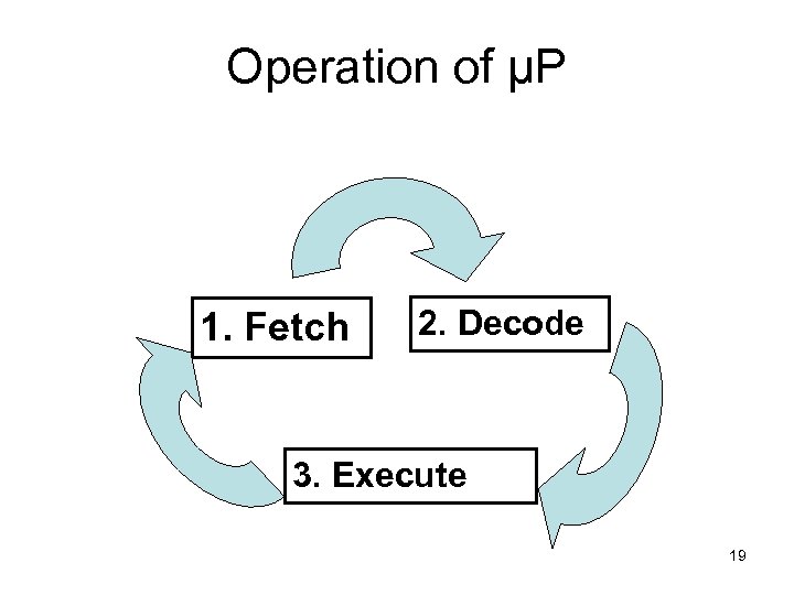 Operation of µP 1. Fetch 2. Decode 3. Execute 19
 Computer Operation (cont…) • The combined fetch-decode-execute operation of a single instruction is known as Instruction Cycle • The portion of a cycle identified with a clearly defined activity is called a State • The interval between pulses of the timing oscillator is known as Clock Period • As a general rule, one or more clock periods are necessary for the completion of a state • And there are several states in a cycle 20
 What is an n-bit processor? • If a processor can operate on n-bit of data simultaneously, then the processor will be called an n-bit processor. • ALU operates on data • So, ALU size determines the size of the processor • 21
 Microprocessor 22
 8086 INTRODUCTION Intel Datasheet Rafiq 3. 1 Hall Brey 26
 8086 Features • First 16 bit processor from Intel –introduced in 1978 –produced from 1978 to 1990 s • CPU clock speed 5 MHz to 10 MHz • Packaged in 40 -pin DIP • 8 general purpose register • prefetches up to 6 instructions from memory and queues them within the chip to speed up execution 27
 8086 Features. . . • 16 bit data bus • 20 bit address bus –can address up to 1 MB memory –Intel has 2 peculiarities in accessing memory • memory must be divided in to 2 banks • instead of a flat memory, it uses segmented memory • 21 bit control bus • most of the lines/pins are used for more than one purpose –hence they are multiplexed 28
 8086 INTERNAL ARCHITECTURE Rafiq 3. 2 Hall ch 2 p/29 Brey 2. 1 29
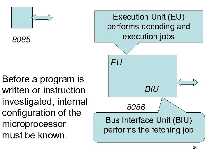 8085 Execution Unit (EU) performs decoding and execution jobs EU Before a program is written or instruction investigated, internal configuration of the microprocessor must be known. BIU 8086 Bus Interface Unit (BIU) performs the fetching job 30
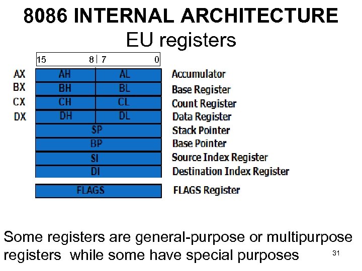 8086 INTERNAL ARCHITECTURE EU registers 15 8 7 0 Some registers are general-purpose or multipurpose 31 registers while some have special purposes
 AX (ACCUMULATOR) • A multipurpose Register • The accumulator is also used for some special purposes such as multiplication, division, some of the adjustment instructions and IN/OUT I/O operations. • Can be used as 16 -bit register (AX), or as either of two 8 -bit registers (AH and AL). 32
 BX (BASE INDEX) • A multipurpose Register • Also used to hold offset address of a location in the memory. • Can be used as 16 -bit register (BX), or as either of two 8 -bit registers (BH and BL). 33
 CX (count) • A multipurpose Register • Also holds the count for various instructions that use a count – repeated string instructions REP, REPE, REPNE use CX – LOOP instruction uses CX – shift and rotate instructions use CL • Can be used as 16 -bit register (CX), or as either of two 8 -bit registers (CH and CL). 34
 DX (data) • A multipurpose Register • Also has some special use – holds a part of the result after multiplication – or part of the dividend before a division. • Can be used as 16 -bit register (DX), or as either of two 8 -bit registers (DH and DL). 35
 SP (Stack Pointer) • Intel categorized it as a multipurpose Register • But it is assigned a special function • it points to an area of memory called the stack. • The stack memory is a LIFO data structure. 36
 BP (Base Pointer) • A multipurpose Register • Can also point to a memory location for memory data transfers. 37
 DI (Destination index) • A multipurpose Register • Often addresses string destination data for the string instruction. 38
 SI (Source index) • A multipurpose Register • Often used to the address source string data for the string instructions. 39
 FLAGS • A special purpose register • Status flags Indicate the condition of the microprocessor • Some of the flags are also used to control the microprocessor. • Most arithmetic and logic operations change the status flags • Status flags never change for any data transfer or program control operation. 40
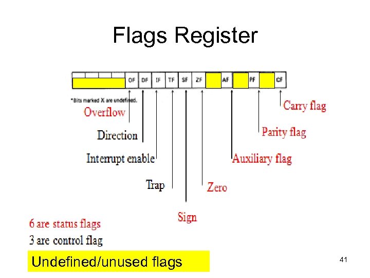 Flags Register Undefined/unused flags 41
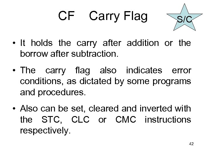 CF Carry Flag S/C • It holds the carry after addition or the borrow after subtraction. • The carry flag also indicates error conditions, as dictated by some programs and procedures. • Also can be set, cleared and inverted with the STC, CLC or CMC instructions respectively. 42
 PF Parity Flag S • Parity is the count of ones in accumulator AL or AX – expressed as even or odd. – Logic 0 for odd parity; logic 1 for even parity. – if a number contains no one bits, it has even parity • Set by most instructions if the least significant eight bits of the destination operand contain an even number of 1 bits. • Today this is seldom used, initially implemented to check data during communication. Today this is mostly done through external hardware rather than the P. 43
 AF Auxiliary Flag S • The auxiliary carry holds the carry (halfcarry) after addition or the borrow after subtraction between bits positions 3 and 4 • This highly specialized flag is used by DAA or DAS instructions during BCD operations. • Otherwise this flag is not used by any other instruction or P 44
 ZF Zero Flag S • The zero flag shows whether the result of an arithmetic or logical operation is zero or not. – When Z = 1, the result is zero. – When Z = 0, the result was non-zero. 45
 SF Sign Flag S • The sign flag holds the arithmetic sign after an arithmetic or a logical operation. • If S =1 the sign bit is set and the result is negative. • If S = 0, the sign bit is not set and the result is positive. 46
 TF Trap / Trace Flag C • It enables trapping through an on-chip debugging facility. • When set to 1 the P interrupts operation based on values set in the debugging register and the control registers. • On being set it allows single-step through programs i. e. , executes exactly one instruction and generates an internal exception 47
 TF Trap / Trace Flag. . . C • Unlike other control flags it cannot be set or clear directly • indirect procedure: – by calling INT 1 OR – pushing flag register in stack using PUSHF – poping in any general purpose register, say AX – manipulating the T-bit with AND/OR operation – pushing it in the stack – poping to flag register using POPF 48
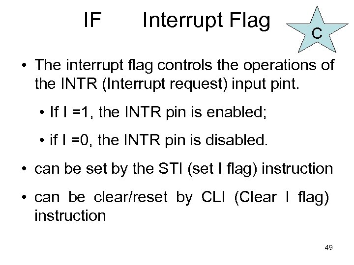 IF Interrupt Flag C • The interrupt flag controls the operations of the INTR (Interrupt request) input pint. • If I =1, the INTR pin is enabled; • if I =0, the INTR pin is disabled. • can be set by the STI (set I flag) instruction • can be clear/reset by CLI (Clear I flag) instruction 49
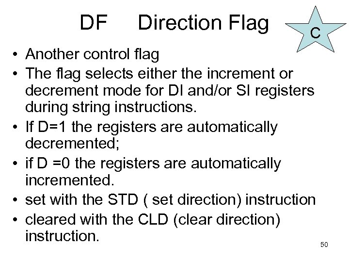 DF Direction Flag C • Another control flag • The flag selects either the increment or decrement mode for DI and/or SI registers during string instructions. • If D=1 the registers are automatically decremented; • if D =0 the registers are automatically incremented. • set with the STD ( set direction) instruction • cleared with the CLD (clear direction) instruction. 50
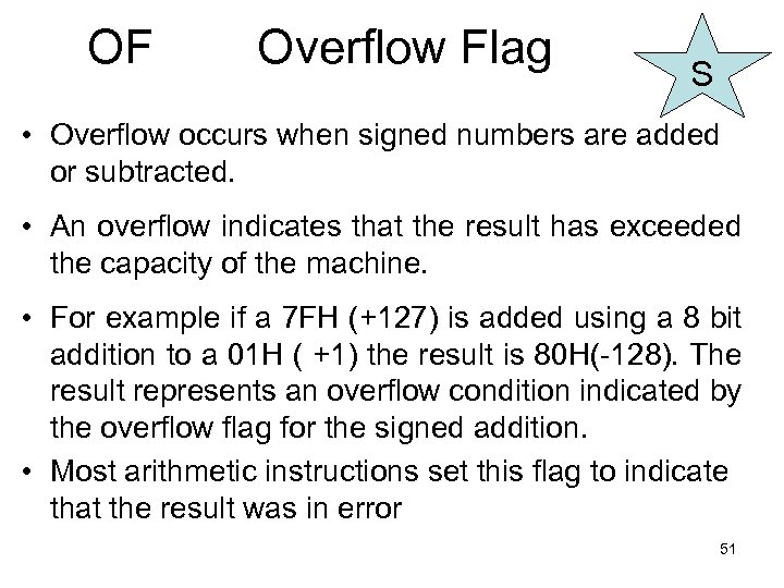 OF Overflow Flag S • Overflow occurs when signed numbers are added or subtracted. • An overflow indicates that the result has exceeded the capacity of the machine. • For example if a 7 FH (+127) is added using a 8 bit addition to a 01 H ( +1) the result is 80 H(-128). The result represents an overflow condition indicated by the overflow flag for the signed addition. • Most arithmetic instructions set this flag to indicate that the result was in error 51
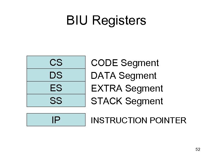 BIU Registers CS DS ES SS CODE Segment DATA Segment EXTRA Segment STACK Segment IP INSTRUCTION POINTER 52
 Segment Registers • Generate memory addresses when combined with other registers in the microprocessor. • Following is a list of each segment register, along with its function in the system. 53
 CS Code Segment Register • The code segment is a section of memory that holds the code (programs and procedures) used by the microprocessor. • The code segment (CS) register defines the starting address of the section of memory holding code. • The code segment size is limited to max 64 KB 54
 DS Data Segment Register • The data segment contains most data used by a program. • The data segment (DS) register defines the starting address of the section of memory holding data. • The data segment size is limited to max 64 KB • Data are accessed in the data segment by an offset address or the contents of other registers that hold the offset address. 55
 ES Extra Segment Register • ES (extra) is an additional data segment used by some of the string instructions to hold destination data. • The extra segment (ES) register defines the starting address of the section of memory used as extra segment • Can be used as an extra/additional segment for code or data • Max size of the segment is limited to 64 KB 56
 SS Stack Segment Register • The stack segment defines the area of memory used for the stack. • The stack segment (SS) register defines the starting address of the section of memory used as stack • The stack entry point is determined by the stack segment and stack pointer registers. • The BP registers also addresses data within the stack segment. 57
 IP Instruction Pointer • Special–Purpose Registers • The Instruction pointer, which points to the next instruction in a program, is used by the microprocessor to find the next sequential instruction in a program located within the code segment. • The instruction pointer can be modified with a jump or a call instruction. 58
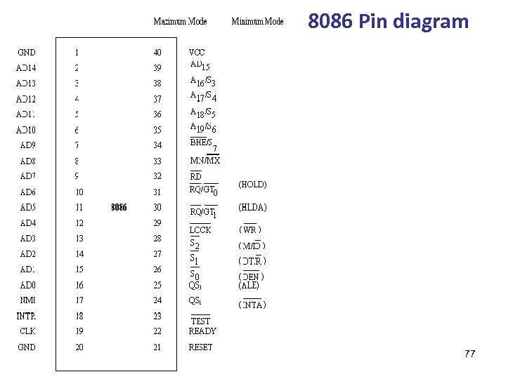
 8086 signals Brey Rafiq 9. 1 3. 8. 1 59
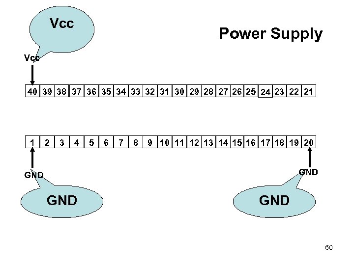 Vcc Power Supply Vcc 40 39 38 37 36 35 34 33 32 31 30 29 28 27 26 25 24 23 22 21 1 2 3 4 5 6 7 8 9 10 11 12 13 14 15 16 17 18 19 20 GND GND 60
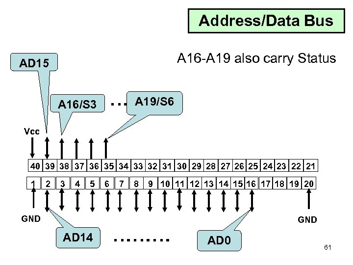 Address/Data Bus A 16 -A 19 also carry Status AD 15 A 16/S 3 … A 19/S 6 Vcc 40 39 38 37 36 35 34 33 32 31 30 29 28 27 26 25 24 23 22 21 1 2 3 4 5 6 7 8 9 10 11 12 13 14 15 16 17 18 19 20 GND AD 14 ……… GND AD 0 61
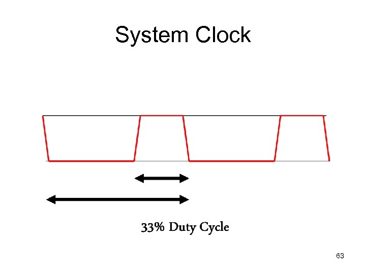
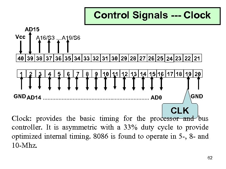 Control Signals --- Clock AD 15 Vcc A 16/S 3 …A 19/S 6 40 39 38 37 36 35 34 33 32 31 30 29 28 27 26 25 24 23 22 21 1 2 3 4 5 6 7 8 9 10 11 12 13 14 15 16 17 18 19 20 GND AD 14. . . . . AD 0 GND CLK Clock: provides the basic timing for the processor and bus controller. It is asymmetric with a 33% duty cycle to provide optimized internal timing. 8086 is found to operate in 5 -, 8 - and 10 -Mhz. 62
 System Clock 63
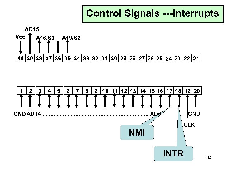 Control Signals ---Interrupts AD 15 Vcc A 16/S 3 …A 19/S 6 40 39 38 37 36 35 34 33 32 31 30 29 28 27 26 25 24 23 22 21 1 2 3 4 5 6 7 8 9 10 11 12 13 14 15 16 17 18 19 20 GND AD 14. . . . . AD 0 NMI GND CLK INTR 64
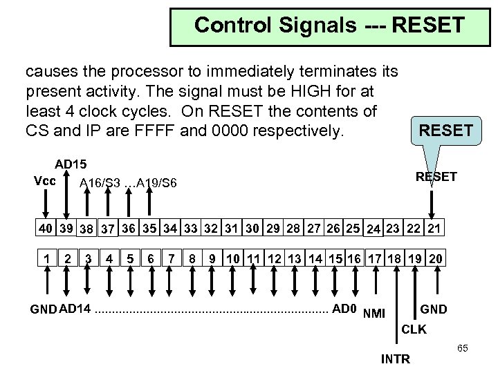 Control Signals --- RESET causes the processor to immediately terminates its present activity. The signal must be HIGH for at least 4 clock cycles. On RESET the contents of CS and IP are FFFF and 0000 respectively. RESET AD 15 Vcc A 16/S 3 …A 19/S 6 RESET 40 39 38 37 36 35 34 33 32 31 30 29 28 27 26 25 24 23 22 21 1 2 3 4 5 6 7 8 9 10 11 12 13 14 15 16 17 18 19 20 GND AD 14. . . . . AD 0 NMI GND CLK INTR 65
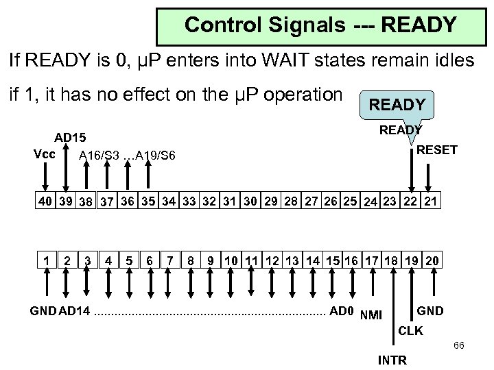 Control Signals --- READY If READY is 0, μP enters into WAIT states remain idles if 1, it has no effect on the μP operation READY AD 15 Vcc A 16/S 3 …A 19/S 6 RESET 40 39 38 37 36 35 34 33 32 31 30 29 28 27 26 25 24 23 22 21 1 2 3 4 5 6 7 8 9 10 11 12 13 14 15 16 17 18 19 20 GND AD 14. . . . . AD 0 NMI GND CLK 66 INTR
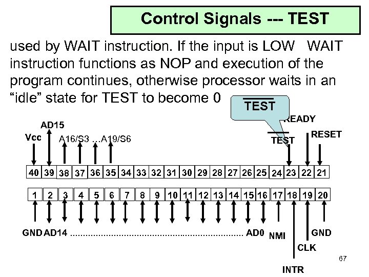 Control Signals --- TEST used by WAIT instruction. If the input is LOW WAIT instruction functions as NOP and execution of the program continues, otherwise processor waits in an “idle” state for TEST to become 0 TEST READY AD 15 Vcc A 16/S 3 …A 19/S 6 RESET TEST 40 39 38 37 36 35 34 33 32 31 30 29 28 27 26 25 24 23 22 21 1 2 3 4 5 6 7 8 9 10 11 12 13 14 15 16 17 18 19 20 GND AD 14. . . . . AD 0 NMI GND CLK 67 INTR
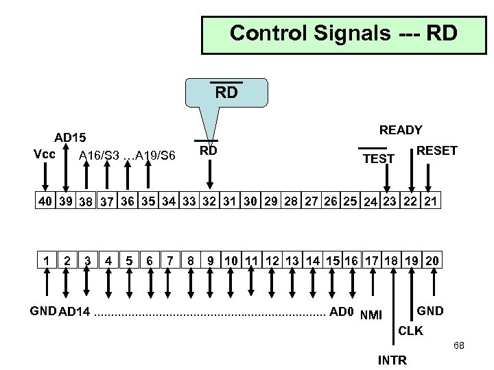 Control Signals --- RD RD READY AD 15 Vcc A 16/S 3 …A 19/S 6 RD RESET TEST 40 39 38 37 36 35 34 33 32 31 30 29 28 27 26 25 24 23 22 21 1 2 3 4 5 6 7 8 9 10 11 12 13 14 15 16 17 18 19 20 GND AD 14. . . . . AD 0 NMI GND CLK 68 INTR
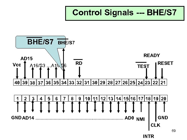 Control Signals --- BHE/S 7 READY AD 15 Vcc A 16/S 3 …A 19/S 6 RD RESET TEST 40 39 38 37 36 35 34 33 32 31 30 29 28 27 26 25 24 23 22 21 1 2 3 4 5 6 7 8 9 10 11 12 13 14 15 16 17 18 19 20 GND AD 14. . . . . AD 0 NMI GND CLK 69 INTR
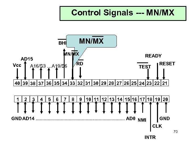 Control Signals --- MN/MX BHE/S 7 MN/MX AD 15 Vcc A 16/S 3 …A 19/S 6 READY RD RESET TEST 40 39 38 37 36 35 34 33 32 31 30 29 28 27 26 25 24 23 22 21 1 2 3 4 5 6 7 8 9 10 11 12 13 14 15 16 17 18 19 20 GND AD 14. . . . . AD 0 NMI GND CLK 70 INTR
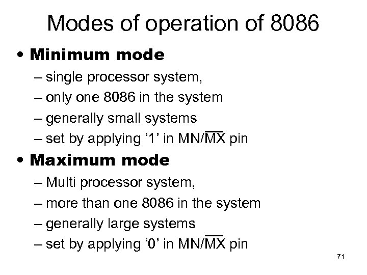 Modes of operation of 8086 • Minimum mode – single processor system, – only one 8086 in the system – generally small systems – set by applying ‘ 1’ in MN/MX pin • Maximum mode – Multi processor system, – more than one 8086 in the system – generally large systems – set by applying ‘ 0’ in MN/MX pin 71
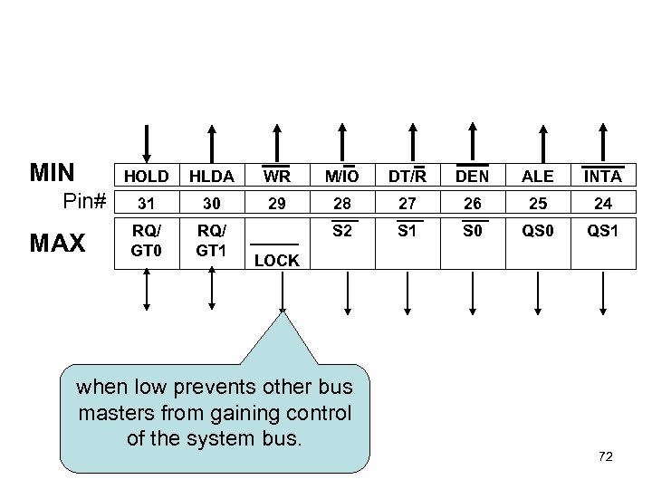 MIN HOLD Pin# MAX HLDA WR M/IO DT/R DEN ALE INTA 31 30 29 28 27 26 25 24 RQ/ GT 0 RQ/ GT 1 S 2 S 1 S 0 QS 1 LOCK when low prevents other bus masters from gaining control of the system bus. 72
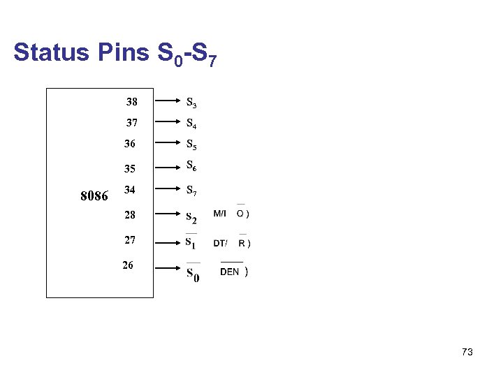 Status Pins S 0 -S 7 38 37 S 4 36 S 5 35 8086 S 3 S 6 34 S 7 28 27 26 73
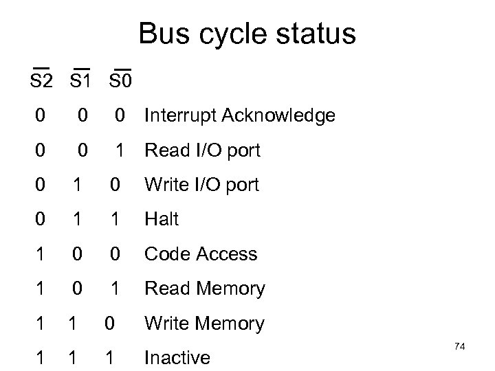 Bus cycle status S 2 S 1 S 0 0 Interrupt Acknowledge 0 0 1 Read I/O port 0 1 0 Write I/O port 0 1 1 Halt 1 0 0 Code Access 1 0 1 Read Memory 1 1 0 Write Memory 1 1 1 Inactive 74
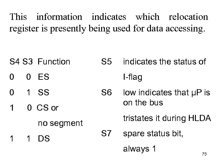 This information indicates which relocation register is presently being used for data accessing. S 4 S 3 Function 0 0 ES 0 1 SS 1 S 5 0 CS or I-flag S 6 1 DS low indicates that µP is on the bus tristates it during HLDA no segment 1 indicates the status of S 7 spare status bit, always 1 75
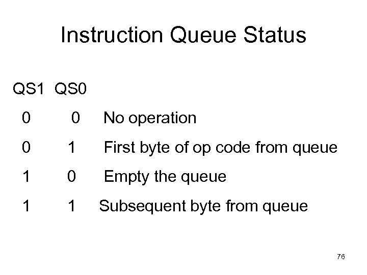 Instruction Queue Status QS 1 QS 0 0 0 No operation 0 1 First byte of op code from queue 1 0 Empty the queue 1 1 Subsequent byte from queue 76
 8086 Pin diagram 77
 8086 Memory Organization Brey Rafiq Hall Ch 2 Ch 3 Ch 2 78
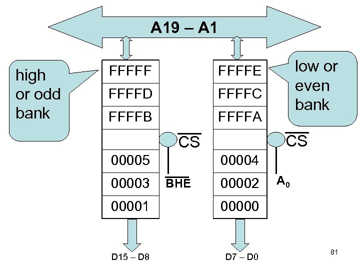
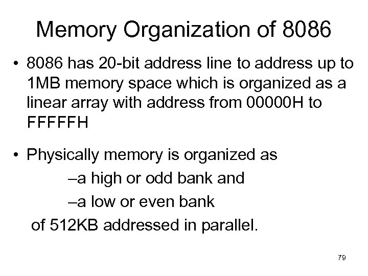 Memory Organization of 8086 • 8086 has 20 -bit address line to address up to 1 MB memory space which is organized as a linear array with address from 00000 H to FFFFFH • Physically memory is organized as –a high or odd bank and –a low or even bank of 512 KB addressed in parallel. 79
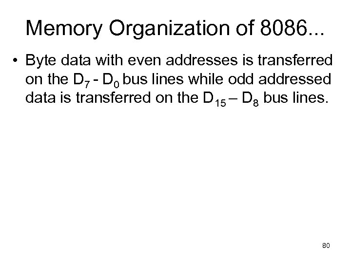 Memory Organization of 8086. . . • Byte data with even addresses is transferred on the D 7 - D 0 bus lines while odd addressed data is transferred on the D 15 – D 8 bus lines. 80
 A 19 – A 1 high or odd bank FFFFFD FFFFC FFFFB low or even bank FFFFE FFFFA CS CS 00005 00003 00004 BHE 00002 00001 00000 D 15 – D 8 D 7 – D 0 A 0 81
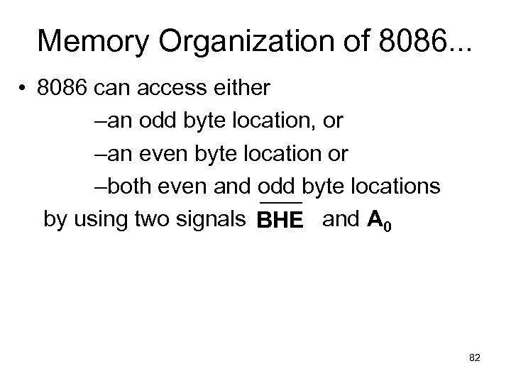 Memory Organization of 8086. . . • 8086 can access either –an odd byte location, or –an even byte location or –both even and odd byte locations by using two signals BHE and A 0 82
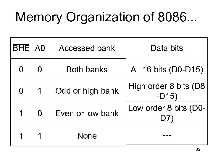 Memory Organization of 8086. . . BHE A 0 0 0 Accessed bank Data bits Both banks All 16 bits (D 0 -D 15) 0 1 Odd or high bank 1 0 Even or low bank 1 1 None High order 8 bits (D 8 -D 15) Low order 8 bits (D 0 D 7) --83
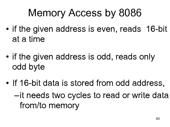 Memory Access by 8086 • if the given address is even, reads 16 -bit at a time • if the given address is odd, reads only odd byte • If 16 -bit data is stored from odd address, – it needs two cycles to read or write data from/to memory 84
 8086 Memory Addressing • As said earlier Intel do not view this 1 MB memory as a flat address from 00000 h to FFFFFh • Rather they use a concept known as Segment: Offset concept • The entire 1 M memory is divided into segments of maxm size 64 KB • Memory segments can touch or even overlap if 64 K bytes of memory are not required for a segment. 85
 Segment and Offsets • Combination of a segment address and an offset address access a memory location. • The segment address located in one segment register defines the beginning address of any 64 K-byte memory segment. • The offset address is also held in a register and selects any location within the 64 K byte memory segment. 86
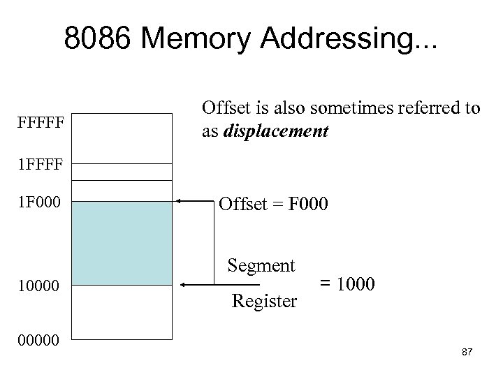 8086 Memory Addressing. . . FFFFF Offset is also sometimes referred to as displacement 1 FFFF 1 F 000 Offset = F 000 Segment 100000 Register = 1000 87
 8086 Memory Addressing. . . • The segment register in the previous example contained 1000 H yet it addresses a segment starting at location 10000 H. • the segment register is always appended with a 0 H on its rightmost end. • Because of the append, segments can begin only at 16 -byte boundary in the memory system. This 16 -byte boundary is called a paragraph. Ø 88
 8086 Memory Addressing. . . • A memory location pointed by a segment address of 1000 H and offset address of 2000 H is written as 1000: 2000. • What is the actual/physical location for 1000: 2000? memory 89
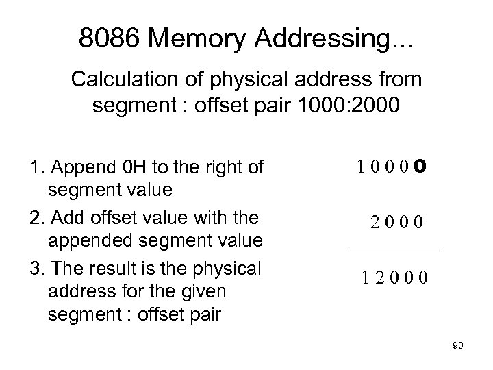 8086 Memory Addressing. . . Calculation of physical address from segment : offset pair 1000: 2000 1. Append 0 H to the right of segment value 2. Add offset value with the appended segment value 3. The result is the physical address for the given segment : offset pair 10000 2000 12000 90
 Default Segment and Offset Registers • 8086 has a set of rules that apply to segments whenever memory is addressed. • These rules define the segment and offset register combination 91
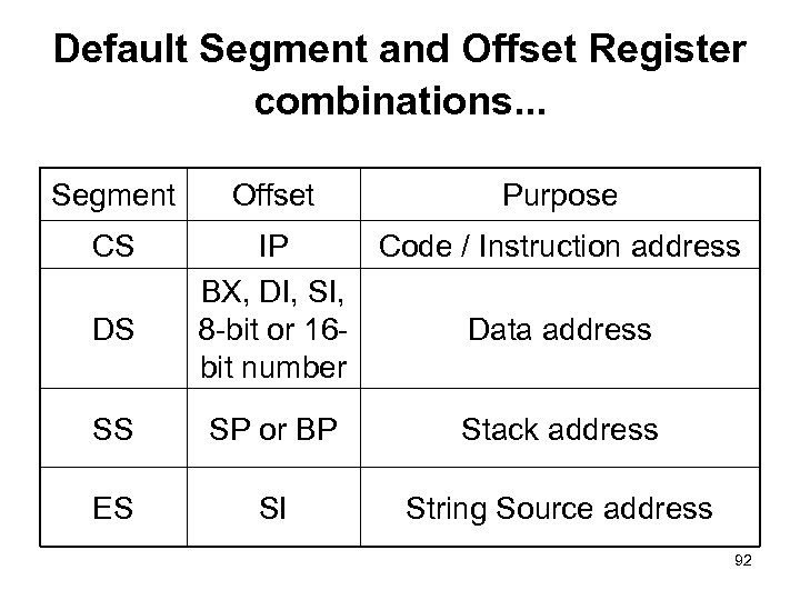 Default Segment and Offset Register combinations. . . Segment CS DS Offset Purpose IP Code / Instruction address BX, DI, SI, 8 -bit or 16 Data address bit number SS SP or BP Stack address ES SI String Source address 92
 8086 Memory Addressing. . . Advantages of segmentation • Segment and offset addressing scheme seems complicated. • But, it has its advantages as well. ØAllows Relocation of üprogram and üdata 93
 8086 Memory Addressing. . . • This is ideal for use in general-purpose computer system in which not all machines contain the same memory areas. • The structure of the personal computer memory structure is different form machine to machine requiring relocateable software and data. 94
 Segment and Offset Addressing Scheme Allows Relocation • A relocatable program is one that can be placed into any area of memory and executed without any change. • Relocatable data are data that can be placed in any area of memory and used without any change to the program. 95
 8086 Memory Addressing. . . • Because memory is addressed within a segment by an offset address, the memory segment can be moved to any place in the memory system without changing any of the offset addresses. • Only the contents of the segment register must be changed to address the program in the new area of memory. 96
 Watch out!!! • 8086 produces a 20 -bit external or effective or physical address from the 32 -bit segment: offset pair. • As a result, each external address can be referred to by 212 = 4096 different segment: offset pairs. 97
 8086 Addressing Modes Rafiq Brey 3. 3 ch 3 98
 Categories of addressing modes Addressing modes of 8086 can be divided into the following categories: 1. addressing Data 2. addressing Program codes in memory 3. addressing Stack in memory 4. addressing I/O 5. Implied addressing 99
![1. addressing Data I. III. IV. V. VII. Immediate addressing Direct addressing Register [direct] 1. addressing Data I. III. IV. V. VII. Immediate addressing Direct addressing Register [direct]](https://present5.com/presentation/bb89a8be52626900a7ea0038efd104df/image-97.jpg) 1. addressing Data I. III. IV. V. VII. Immediate addressing Direct addressing Register [direct] addressing Register indirect addressing Base-plus-index addressing Register relative addressing Base-relative-plus-index addressing 100
1. addressing Data I. III. IV. V. VII. Immediate addressing Direct addressing Register [direct] addressing Register indirect addressing Base-plus-index addressing Register relative addressing Base-relative-plus-index addressing 100
 1. addressing Data (contd. . . ) i) Immediate addressing • Data is immediately given in the instruction MOV AL, 90 101
 1. addressing Data (contd. . . ) ii) Direct addressing • Data address is directly given in the instruction MOV AX, [12345] MOV BX, DATA 102
![1. addressing Data (contd. . . ) iii) Register [direct] addressing • data is 1. addressing Data (contd. . . ) iii) Register [direct] addressing • data is](https://present5.com/presentation/bb89a8be52626900a7ea0038efd104df/image-100.jpg) 1. addressing Data (contd. . . ) iii) Register [direct] addressing • data is in a register (here BX register contains the data) MOV AX, BX 103
1. addressing Data (contd. . . ) iii) Register [direct] addressing • data is in a register (here BX register contains the data) MOV AX, BX 103
 1. addressing Data (contd. . . ) iv) Register indirect addressing • Register supplies the address of the required data MOV CX, [BX] 104
![1. addressing Data (contd. . . ) v) Base-plus-index addressing MOV DX, [BX+DI] • 1. addressing Data (contd. . . ) v) Base-plus-index addressing MOV DX, [BX+DI] •](https://present5.com/presentation/bb89a8be52626900a7ea0038efd104df/image-102.jpg) 1. addressing Data (contd. . . ) v) Base-plus-index addressing MOV DX, [BX+DI] • Base register is either BX or BP • Index register is either DI or SI 105
1. addressing Data (contd. . . ) v) Base-plus-index addressing MOV DX, [BX+DI] • Base register is either BX or BP • Index register is either DI or SI 105
![1. addressing Data (contd. . . ) vi) Register relative addressing MOV AX, [BX+1000] 1. addressing Data (contd. . . ) vi) Register relative addressing MOV AX, [BX+1000]](https://present5.com/presentation/bb89a8be52626900a7ea0038efd104df/image-103.jpg) 1. addressing Data (contd. . . ) vi) Register relative addressing MOV AX, [BX+1000] • Register can be a base (BX, BP) or an index register (DI, SI) • Mainly suitable to address array data 106
1. addressing Data (contd. . . ) vi) Register relative addressing MOV AX, [BX+1000] • Register can be a base (BX, BP) or an index register (DI, SI) • Mainly suitable to address array data 106
![1. addressing Data (contd. . . ) vii) Base-relative-plus-index addressing MOV AX, [BX+DI+10] • 1. addressing Data (contd. . . ) vii) Base-relative-plus-index addressing MOV AX, [BX+DI+10] •](https://present5.com/presentation/bb89a8be52626900a7ea0038efd104df/image-104.jpg) 1. addressing Data (contd. . . ) vii) Base-relative-plus-index addressing MOV AX, [BX+DI+10] • suitable for array addressing 107
1. addressing Data (contd. . . ) vii) Base-relative-plus-index addressing MOV AX, [BX+DI+10] • suitable for array addressing 107
 2. • • addressing Program codes in memory used with JMP and CALL instructions 3 distinct forms: – direct – indirect – relative 108
 addressing Program codes. . . direct • address is directly given in the instruction JMP 1000: 1000 CALL 1000: 1000 • JMP doagain CALL doagain often known as far jump or far call 109
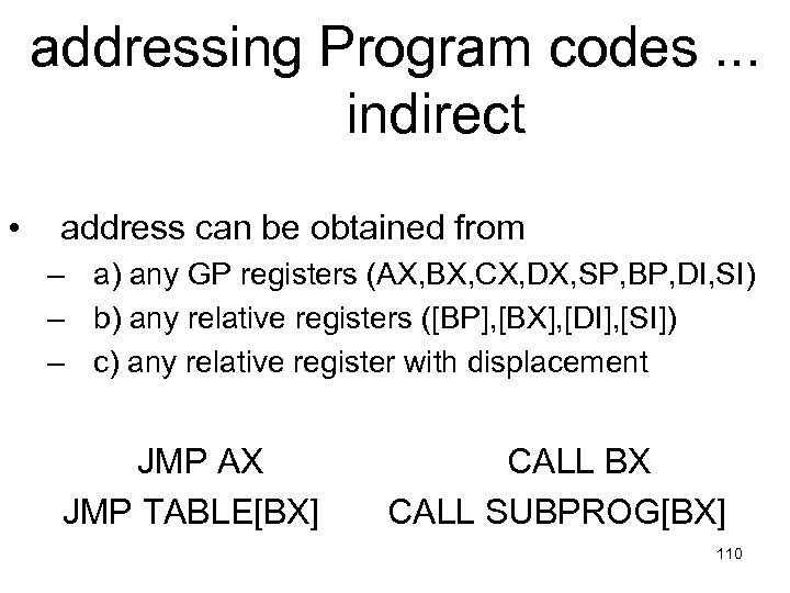 addressing Program codes. . . indirect • address can be obtained from – a) any GP registers (AX, BX, CX, DX, SP, BP, DI, SI) – b) any relative registers ([BP], [BX], [DI], [SI]) – c) any relative register with displacement JMP AX JMP TABLE[BX] CALL BX CALL SUBPROG[BX] 110
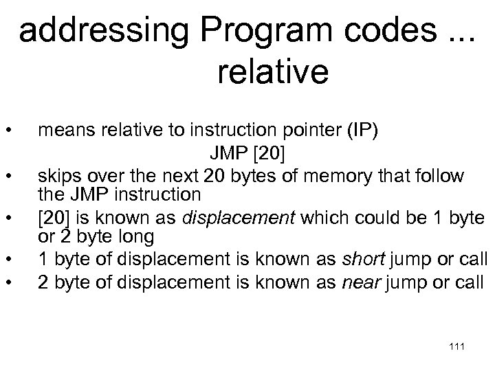 addressing Program codes. . . relative • • • means relative to instruction pointer (IP) JMP [20] skips over the next 20 bytes of memory that follow the JMP instruction [20] is known as displacement which could be 1 byte or 2 byte long 1 byte of displacement is known as short jump or call 2 byte of displacement is known as near jump or call 111
 3. addressing Stack in memory • PUSH and POP instructions are used to move data to and from stack. • CALL also uses the stack to hold return address for procedure 112
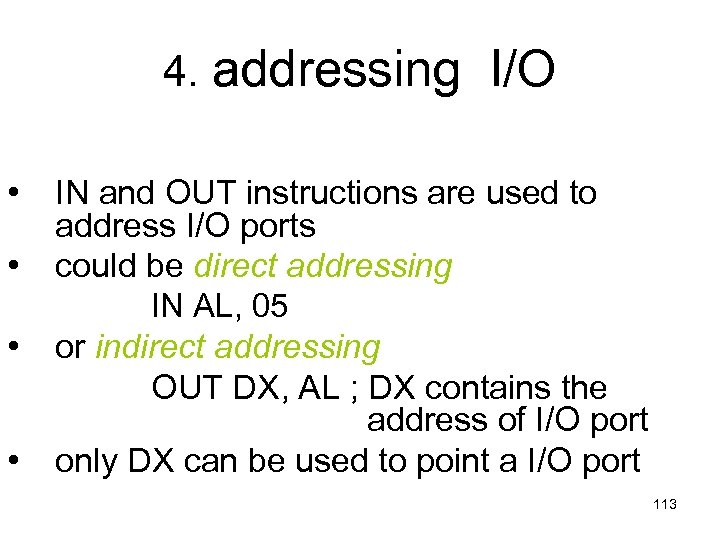 4. addressing I/O • • IN and OUT instructions are used to address I/O ports could be direct addressing IN AL, 05 or indirect addressing OUT DX, AL ; DX contains the address of I/O port only DX can be used to point a I/O port 113
 5. Implied addressing CLC ; clear carry flag • • NO explicit address is given with the instruction implied within the instruction itself 114
 8086 INSTRUCTION SET 115
 Instruction Set • You have studied it in CSE 214. So we will skip it here. • Includes equivalents of 8085 instruction set plus many new ones • Has approx 117 different instructions – with about 300 different op codes 116
 Instruction Set (cont…) • Instructions contain – no operand, CLC, CLD, CLI, NOP – single operand, INC AX and – two operands MOV AX, BX • Except for string instructions which involve array operations, 8086 does not permit memory -to-memory operations 117
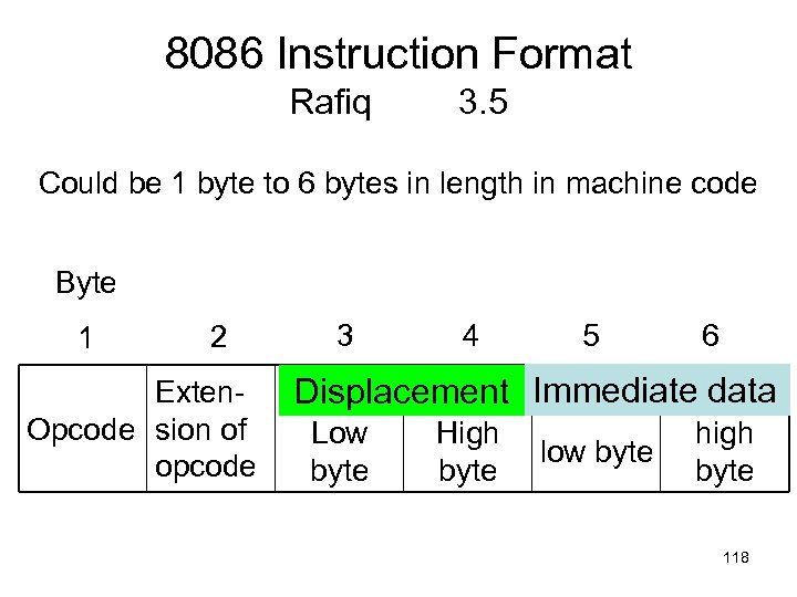 8086 Instruction Format Rafiq 3. 5 Could be 1 byte to 6 bytes in length in machine code Byte 1 2 Exten. Opcode sion of opcode 3 4 5 6 Displacement Immediate data Low byte High byte low byte high byte 118
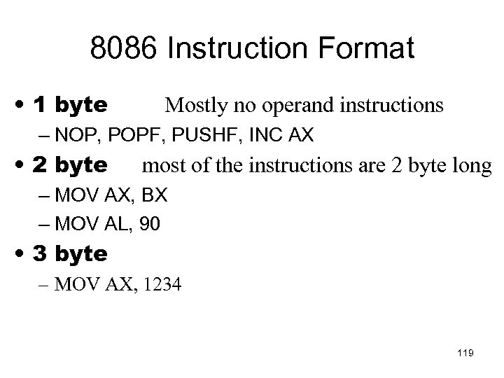 8086 Instruction Format • 1 byte Mostly no operand instructions – NOP, POPF, PUSHF, INC AX • 2 byte most of the instructions are 2 byte long – MOV AX, BX – MOV AL, 90 • 3 byte – MOV AX, 1234 119
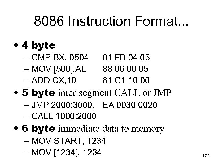 8086 Instruction Format. . . • 4 byte – CMP BX, 0504 – MOV [500], AL – ADD CX, 10 81 FB 04 05 88 06 00 05 81 C 1 10 00 • 5 byte inter segment CALL or JMP – JMP 2000: 3000, EA 0030 0020 – CALL 1000: 2000 • 6 byte immediate data to memory – MOV START, 1234 – MOV [1234], 1234 120
 8086 INTERRUPT üBrey üRafiq üHall Ch 12 Interrupts 3. 9 Interrupts Ch 8 121
 What is an interrupt? • capability to suspend the execution of running program and execution of another program to fulfill specific requirement upon request • after finishing the second program, automatically return to the first program and start execution from where it was left 122
 Why interrupt capability is necessary? • To understand this we will have to review how µP/µC communicate with the outside world. 123
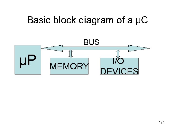 Basic block diagram of a µC BUS µP MEMORY I/O DEVICES 124
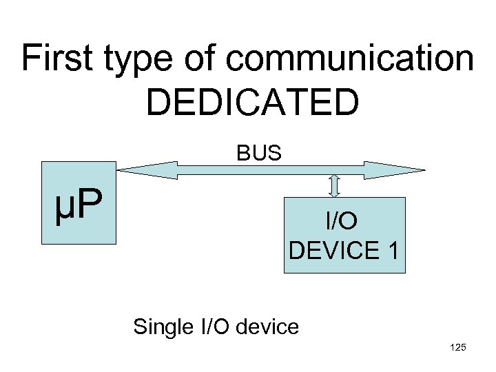 First type of communication DEDICATED BUS µP I/O DEVICE 1 Single I/O device 125
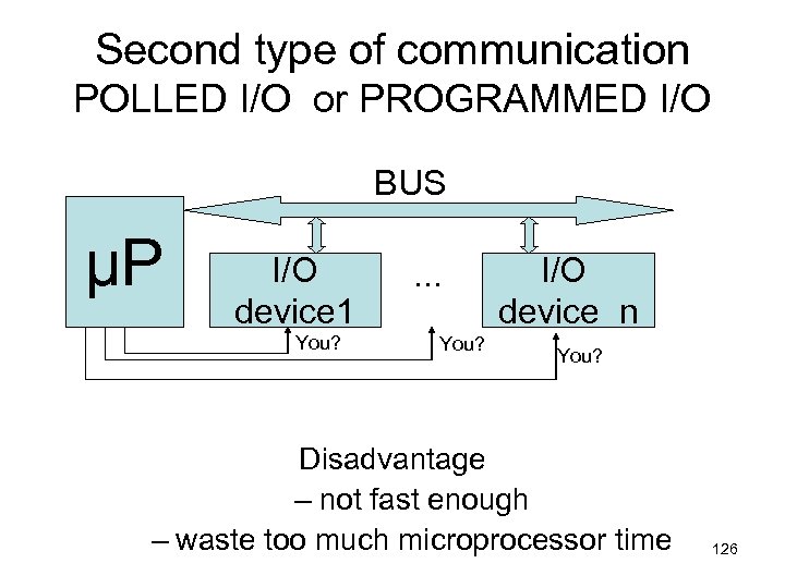 Second type of communication POLLED I/O or PROGRAMMED I/O BUS µP I/O device 1 You? . . . You? I/O device n You? Disadvantage – not fast enough – waste too much microprocessor time 126
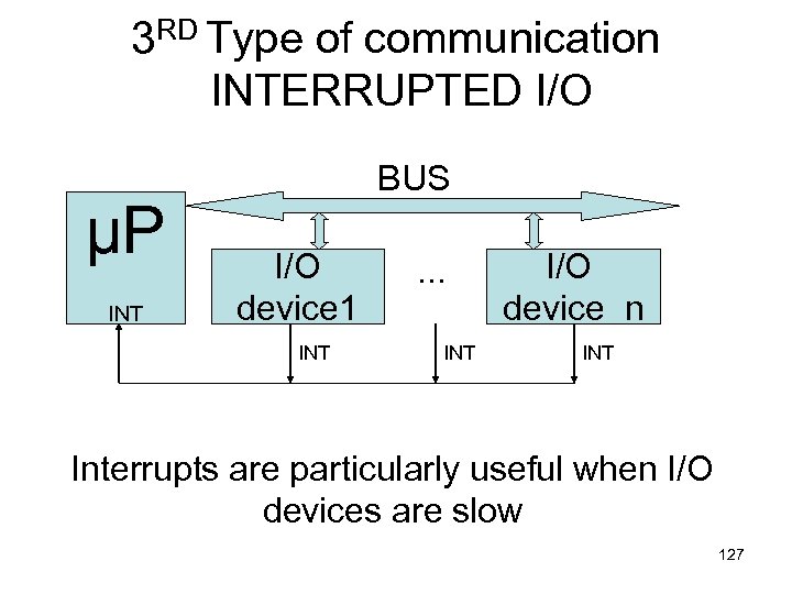 3 RD Type of communication INTERRUPTED I/O µP INT BUS I/O device 1 INT . . . INT I/O device n INT Interrupts are particularly useful when I/O devices are slow 127
 • Most microprocessors allow normal program execution to be interrupted by some external signal or by a special instruction in the program. • In response to an interrupt, the microprocessor stops executing its current program and calls a procedure which “services” the interrupt. • A special instruction --- IRET --- at the end of interrupt-service procedure returns execution to the interrupted main program. 128
 8086 interrupts can be classified into two types: • 1) Predefined interrupt some error condition produced by execution of an instruction, e. g. , trying to divide some number by zero. • 2) User defined interrupt – i) hardware interrupt – An external signal applied to INTR pin – ii) software interrupt – execution of interrupt instruction INT 130
 • At the end of each instruction cycle, 8086 checks to see if any interrupts have been requested. • If yes, then 8086 responds to the interrupt by stepping through the following series of major actions: 131
 1. It decremented SP by 2 and pushes Flag register on the stack. 2. It disables 8086 INTR input by clearing IF flag in Flag register 3. It resets the TF (trap) flag in Flag register 4. It decremented SP again by 2 and pushes current CS contents on the stack. 5. It decremented SP again by 2 and pushes current IP contents on the stack. 6. It does an indirect far jump to the start of the procedure written to respond to the interrupt. 132
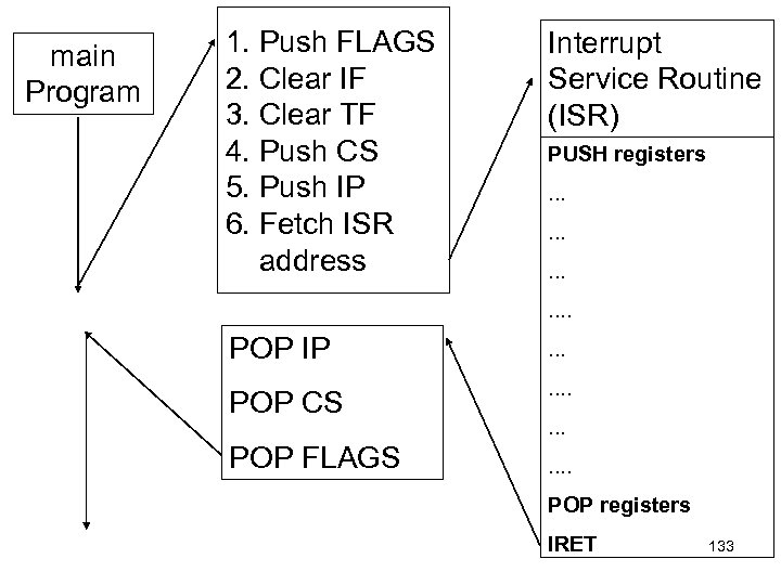 main Program 1. Push FLAGS 2. Clear IF 3. Clear TF 4. Push CS 5. Push IP 6. Fetch ISR address Interrupt Service Routine (ISR) PUSH registers. . . POP IP . . . POP CS . . POP FLAGS . . . . POP registers IRET 133
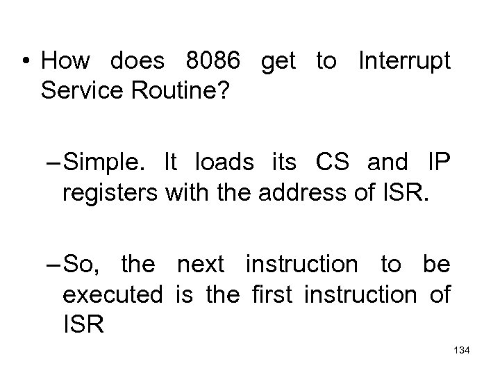 • How does 8086 get to Interrupt Service Routine? – Simple. It loads its CS and IP registers with the address of ISR. – So, the next instruction to be executed is the first instruction of ISR 134
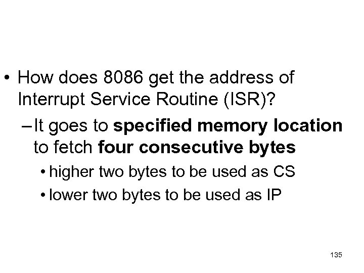 • How does 8086 get the address of Interrupt Service Routine (ISR)? – It goes to specified memory location to fetch four consecutive bytes • higher two bytes to be used as CS • lower two bytes to be used as IP 135
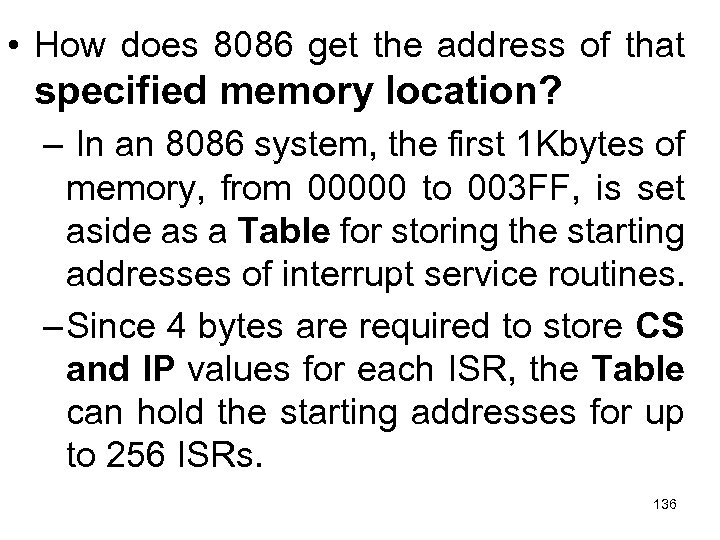 • How does 8086 get the address of that specified memory location? – In an 8086 system, the first 1 Kbytes of memory, from 00000 to 003 FF, is set aside as a Table for storing the starting addresses of interrupt service routines. – Since 4 bytes are required to store CS and IP values for each ISR, the Table can hold the starting addresses for up to 256 ISRs. 136
 • The starting address of an ISR is often called – the interrupt vector or – the interrupt pointer. • So the Table is referred to as – interrupt-vector table or – interrupt-pointer table. 137
 • Next slide shows how the 256 interrupt vectors are arranged in the table in memory • Note that – the IP value is put in as the low word of the vector – CS as high word of the vector • Each double word interrupt vector is identified by a number from 0 to 255 • INTEL calls this number the TYPE of the interrupt 138
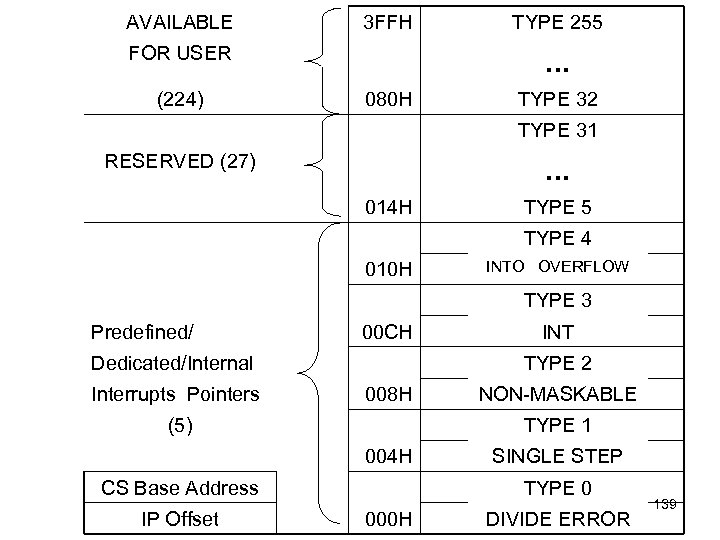 AVAILABLE 3 FFH FOR USER (224) TYPE 255 . . . 080 H TYPE 32 TYPE 31 RESERVED (27) . . . 014 H TYPE 5 TYPE 4 010 H INTO OVERFLOW TYPE 3 Predefined/ 00 CH Dedicated/Internal Interrupts Pointers TYPE 2 008 H (5) NON-MASKABLE TYPE 1 004 H CS Base Address IP Offset INT SINGLE STEP TYPE 0 000 H DIVIDE ERROR 139
 • How does 8086 get the address of a particular ISR? – In an 8086 system, each “interrupter” has an id# – 8086 treat this id# as interruption type# – after receiving INTR signal, 8086 sends an INTA signal – after receiving INTA signal, interrupter releases it’s id#, i. e. , type# of the interruption. 140
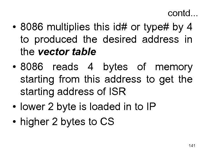 contd. . . • 8086 multiplies this id# or type# by 4 to produced the desired address in the vector table • 8086 reads 4 bytes of memory starting from this address to get the starting address of ISR • lower 2 byte is loaded in to IP • higher 2 bytes to CS 141
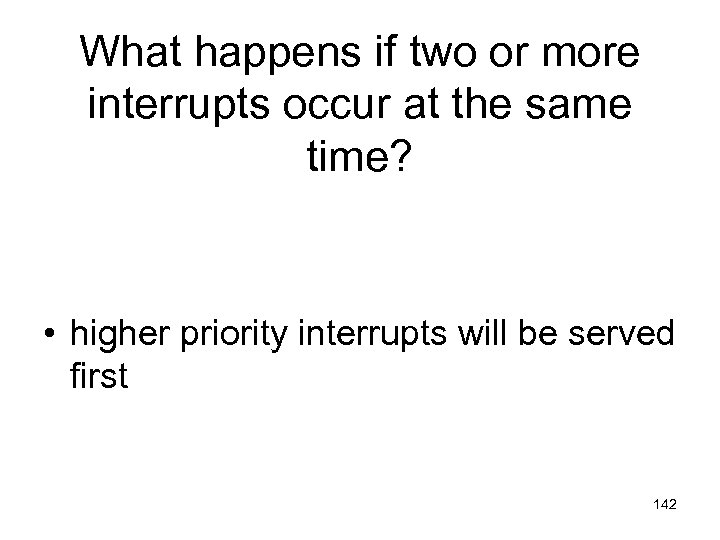 What happens if two or more interrupts occur at the same time? • higher priority interrupts will be served first 142
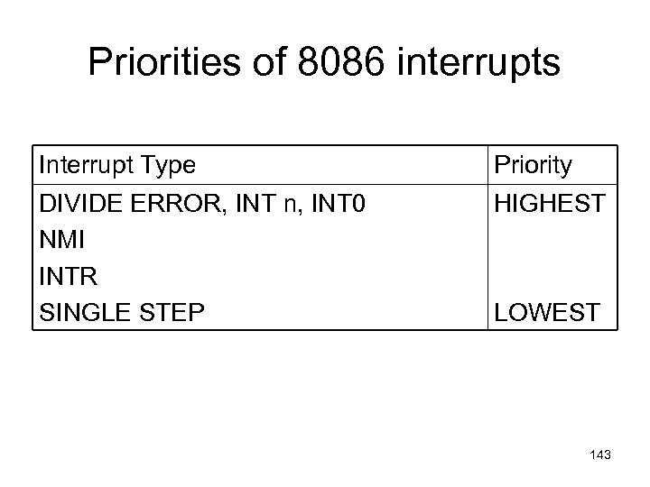 Priorities of 8086 interrupts Interrupt Type Priority DIVIDE ERROR, INT n, INT 0 NMI INTR SINGLE STEP HIGHEST LOWEST 143
 Delay Loop Calculation Hall ch 4 2 nd Edition page 91
 • Each instruction takes a certain number of clock cycles to execute • MOV register to register [mov ax, bx] for example requires 2 clock cycles • If you are running a µP, for example, with a 10 MHz clock, – then each clock cycles takes 1/(10 MHz) or 0. 1µs • An instruction which takes 2 clock cycles, then will take 2 X 0. 1µs or 0. 2 µs to execute
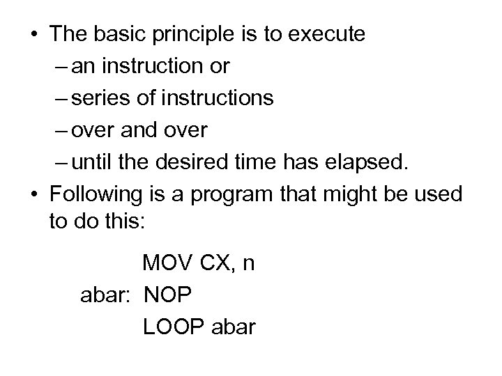 • The basic principle is to execute – an instruction or – series of instructions – over and over – until the desired time has elapsed. • Following is a program that might be used to do this: MOV CX, n abar: NOP LOOP abar
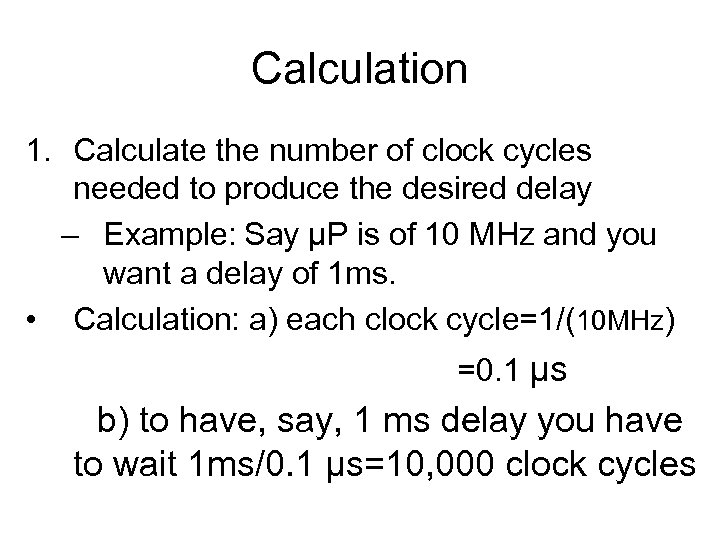 Calculation 1. Calculate the number of clock cycles needed to produce the desired delay – Example: Say µP is of 10 MHz and you want a delay of 1 ms. • Calculation: a) each clock cycle=1/(10 MHz) =0. 1 µs b) to have, say, 1 ms delay you have to wait 1 ms/0. 1 µs=10, 000 clock cycles
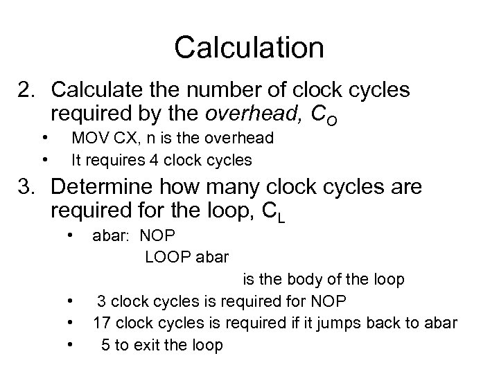 Calculation 2. Calculate the number of clock cycles required by the overhead, CO • • MOV CX, n is the overhead It requires 4 clock cycles 3. Determine how many clock cycles are required for the loop, CL • • abar: NOP LOOP abar is the body of the loop 3 clock cycles is required for NOP 17 clock cycles is required if it jumps back to abar 5 to exit the loop
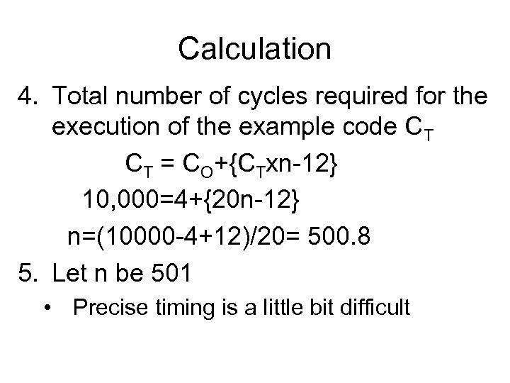 Calculation 4. Total number of cycles required for the execution of the example code CT CT = CO+{CTxn-12} 10, 000=4+{20 n-12} n=(10000 -4+12)/20= 500. 8 5. Let n be 501 • Precise timing is a little bit difficult


