140b27a90f53b189b5ff4b04994a7a07.ppt
- Количество слайдов: 29
 The D 0 Silicon Tracker For the D 0 Collaboration, W. E. Cooper, Fermilab INSTR 08
 D 0 Silicon • Run IIa silicon was commissioned during the spring of 2001. – Run IIa silicon was a learning experience. • First D 0 silicon tracker – Designed for an integrated luminosity of 2 fb-1 – Capability of L 1 (original innermost layer) silicon was more recently estimated to be 3. 5 to 4 fb-1, but with large uncertainties – Even that appears to be too low an estimate – Useful life is expected to be limited by increases in depletion voltage from irradiation and punch through of AC coupling capacitors. • L 0 silicon was completed in August 2005 and installed in spring 2006. – L 0 is a jewel and major technical accomplishment in every respect. – Improves vertex resolution and would preserve silicon tracking after irradiation of Run IIa silicon. – Leakage current calculations indicate a S/N > 12 at -10 o C after an integrated luminosity of 10 fb-1 • Run II goal is 8 fb-1 in 2009. W. E. Cooper, Fermilab INSTR 08 2
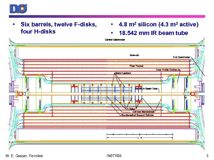 • Six barrels, twelve F-disks, four H-disks W. E. Cooper, Fermilab • 4. 8 m 2 silicon (4. 3 m 2 active) • 18. 542 mm IR beam tube INSTR 08 3
 Run IIa sensors • • • All sensors are AC coupled. Thickness of Run IIa sensors = 300 µm. Barrel sensors were provided by Micron. – 144 9 -chip, double-sided, 2 degree stereo sensors per barrel, 50 m pitch on axial surface, 62. 5 m pitch on stereo surface (± 2 o varieties) – 144 6 -chip, double-sided, 90 degree stereo sensors in the central four barrels, 50 m pitch on axial surface, 153. 5 m pitch on stereo surface – 144 3 -chip, single-sided sensors in outermost barrels, 50 m pitch – Two 60 mm long sensors, end-to-end, per ladder • F-disk sensors were provided by Micron and Eurisys. – Twelve sensors per F-disk – Double-sided, 30 degree stereo, 50 m pitch on p-side, 62. 5 m pitch on nside • H-disk sensors were provided by ELMA (near Moscow) (2 varieties). – Single-sided, mated back to provide 15 degree stereo – Two back to back sensor pairs per wedge, one pair at smaller radius and the second at larger radius – The two sensors of a given wedge surface are wire bonded and share a common readout – 24 wedges per H-disk – 4 sensors per wedge, 80 m pitch with intermediate strips W. E. Cooper, Fermilab INSTR 08 4
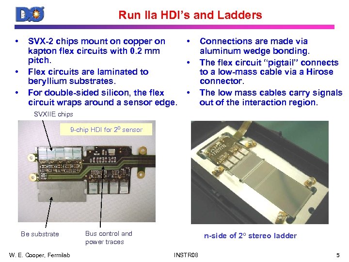 Run IIa HDI’s and Ladders • • • SVX-2 chips mount on copper on kapton flex circuits with 0. 2 mm pitch. Flex circuits are laminated to beryllium substrates. For double-sided silicon, the flex circuit wraps around a sensor edge. • • • Connections are made via aluminum wedge bonding. The flex circuit “pigtail” connects to a low-mass cable via a Hirose connector. The low mass cables carry signals out of the interaction region. SVXIIE chips 9 -chip HDI for 20 sensor Be substrate W. E. Cooper, Fermilab Bus control and power traces n-side of 2 o stereo ladder INSTR 08 5
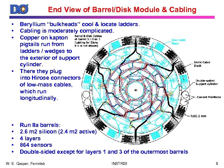 End View of Barrel/Disk Module & Cabling • • • Beryllium “bulkheads” cool & locate ladders. Cabling is moderately complicated. Copper on kapton pigtails run from ladders / wedges to the exterior of support cylinder. There they plug into Hirose connectors of low-mass cables, which run longitudinally. Run IIa barrels: 2. 6 m 2 silicon (2. 4 m 2 active) 4 layers 864 sensors Double-sided except for layers 1 and 3 of the outermost barrels W. E. Cooper, Fermilab INSTR 08 6
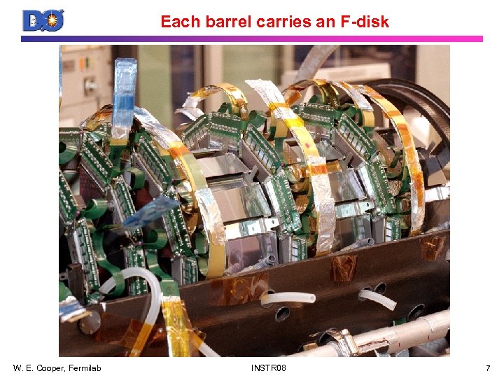 Each barrel carries an F-disk W. E. Cooper, Fermilab INSTR 08 7
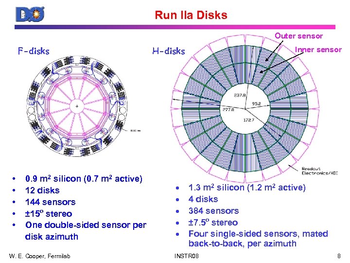 Run IIa Disks Outer sensor F-disks • • • 0. 9 m 2 silicon (0. 7 m 2 active) 12 disks 144 sensors ± 15 o stereo One double-sided sensor per disk azimuth W. E. Cooper, Fermilab H-disks · · · Inner sensor 1. 3 m 2 silicon (1. 2 m 2 active) 4 disks 384 sensors ± 7. 5 o stereo Four single-sided sensors, mated back-to-back, per azimuth INSTR 08 8
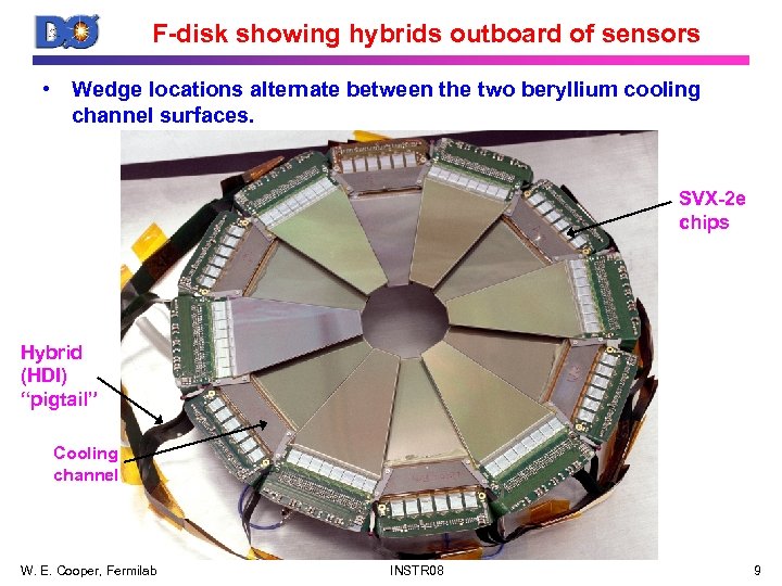 F-disk showing hybrids outboard of sensors • Wedge locations alternate between the two beryllium cooling channel surfaces. SVX-2 e chips Hybrid (HDI) “pigtail” Cooling channel W. E. Cooper, Fermilab INSTR 08 9
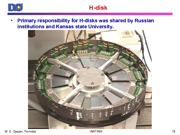 H-disk • Primary responsibility for H-disks was shared by Russian institutions and Kansas state University. W. E. Cooper, Fermilab INSTR 08 10
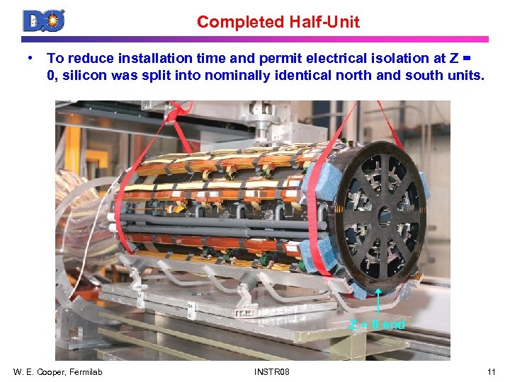 Completed Half-Unit • To reduce installation time and permit electrical isolation at Z = 0, silicon was split into nominally identical north and south units. Z = 0 end W. E. Cooper, Fermilab INSTR 08 11
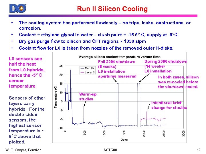 Run II Silicon Cooling • • The cooling system has performed flawlessly – no trips, leaks, obstructions, or corrosion. Coolant = ethylene glycol in water – slush point = -16. 5 o C, supply at -9 o. C. Dry gas purge flow to silicon and CFT regions ~ 1330 slpm Coolant flow for L 0 is taken from nozzles of the removed outer H-disks. L 0 sensors see half the heat from L 0 hybrids, hence the -5 o C sensor temperature. Sensors of other layers carry hybrids. For the double-sided sensors, the highest sensor temperature is ~ 9 o. C above that plotted. W. E. Cooper, Fermilab Fall 2004 shutdown (8 weeks) L 0 installation apertures measured Warm-up studies Spring 2006 shutdown (14 weeks) L 0 installation In both cases, silicon was re-cooled before the shutdown ended. Intentional brief change for studies INSTR 08 12
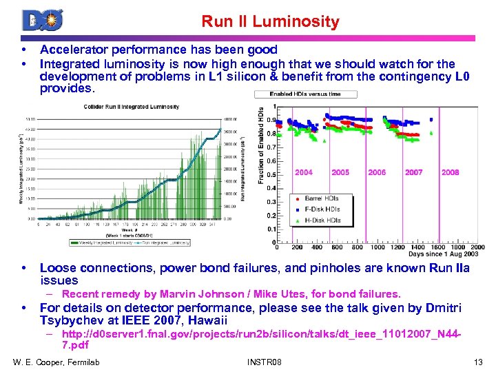 Run II Luminosity • • Accelerator performance has been good Integrated luminosity is now high enough that we should watch for the development of problems in L 1 silicon & benefit from the contingency L 0 provides. • Loose connections, power bond failures, and pinholes are known Run IIa issues – Recent remedy by Marvin Johnson / Mike Utes, for bond failures. • For details on detector performance, please see the talk given by Dmitri Tsybychev at IEEE 2007, Hawaii – http: //d 0 server 1. fnal. gov/projects/run 2 b/silicon/talks/dt_ieee_11012007_N 447. pdf W. E. Cooper, Fermilab INSTR 08 13
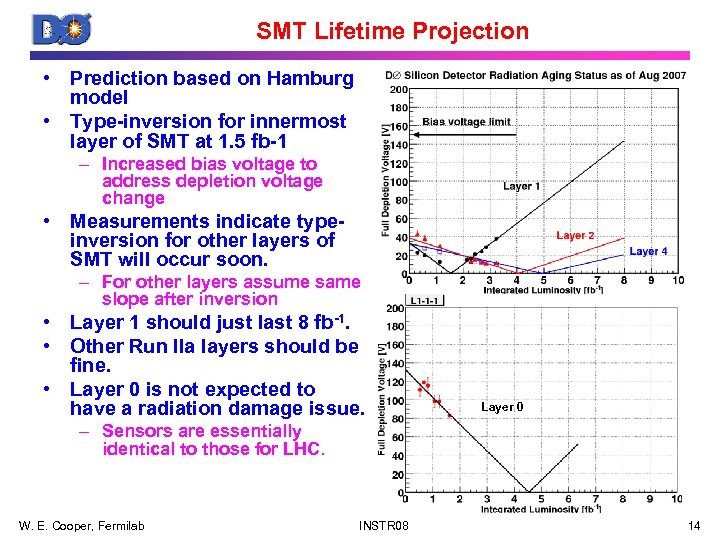 SMT Lifetime Projection • Prediction based on Hamburg model • Type-inversion for innermost layer of SMT at 1. 5 fb-1 – Increased bias voltage to address depletion voltage change • Measurements indicate typeinversion for other layers of SMT will occur soon. – For other layers assume same slope after inversion • Layer 1 should just last 8 fb-1. • Other Run IIa layers should be fine. • Layer 0 is not expected to have a radiation damage issue. Layer 0 – Sensors are essentially identical to those for LHC. W. E. Cooper, Fermilab INSTR 08 14
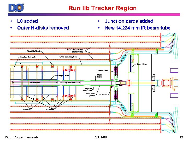 Run IIb Tracker Region • • L 0 added Outer H-disks removed W. E. Cooper, Fermilab • • Junction cards added New 14. 224 mm IR beam tube INSTR 08 15
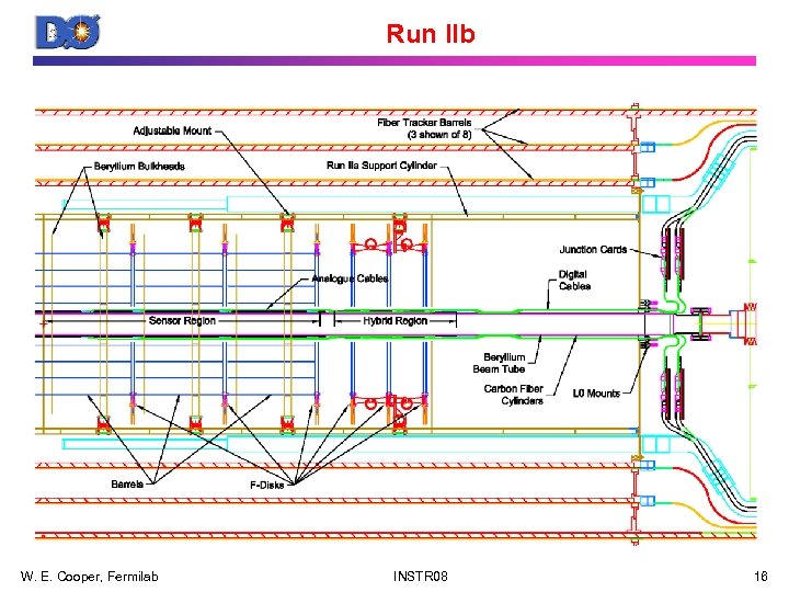 Run IIb W. E. Cooper, Fermilab INSTR 08 16
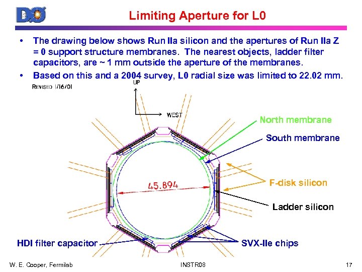 Limiting Aperture for L 0 • • The drawing below shows Run IIa silicon and the apertures of Run IIa Z = 0 support structure membranes. The nearest objects, ladder filter capacitors, are ~ 1 mm outside the aperture of the membranes. Based on this and a 2004 survey, L 0 radial size was limited to 22. 02 mm. North membrane South membrane F-disk silicon Ladder silicon HDI filter capacitor W. E. Cooper, Fermilab SVX-IIe chips INSTR 08 17
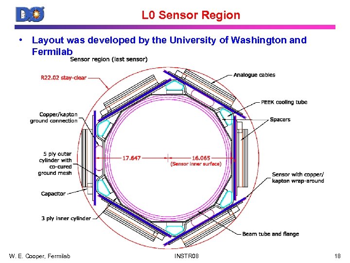 L 0 Sensor Region • Layout was developed by the University of Washington and Fermilab W. E. Cooper, Fermilab INSTR 08 18
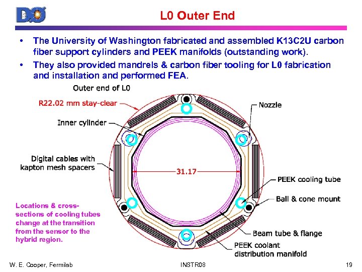 L 0 Outer End • • The University of Washington fabricated and assembled K 13 C 2 U carbon fiber support cylinders and PEEK manifolds (outstanding work). They also provided mandrels & carbon fiber tooling for L 0 fabrication and installation and performed FEA. Locations & crosssections of cooling tubes change at the transition from the sensor to the hybrid region. W. E. Cooper, Fermilab INSTR 08 19
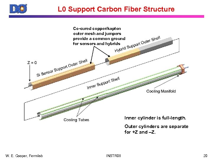 L 0 Support Carbon Fiber Structure Co-cured copper/kapton outer mesh and jumpers provide a common ground for sensors and hybrids Inner cylinder is full-length. Outer cylinders are separate for +Z and –Z. W. E. Cooper, Fermilab INSTR 08 20
 L 0 Sensors • All sensors were obtained from HPK (Hamamatsu Photonics). – 320 µm thick, AC coupled – All are single-sided with intermediate strips and polysilicon biasing. – 120 purchased, 48 used (conservatism based upon 4 varieties of sensors & minimal time to address any problems) • • The overall quality was excellent. HPK tests – IV curve to 800 volts (~ 35 na per sensor at 800 volts at RT) – CV curve to determine FDV (~ 180 volts) – Measure coupling capacitance (> 10 pf/cm) & search for pinholes on every strip – Optical inspection for defects & mask alignment (< 2 µm) – Test structures were used to monitor polysilicon resistance, implant resistance, Al resistance, & AC coupling capacitance • • • IV & CV measurements by D 0 gave acceptable agreement with HPK results. More detailed testing of 4 sensors was performed at Stony Brook. Irradiation tests of those 4 sensors were conducted at Kansas State University. W. E. Cooper, Fermilab INSTR 08 21
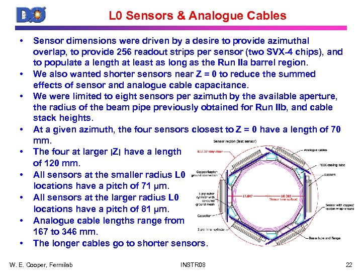 L 0 Sensors & Analogue Cables • • • Sensor dimensions were driven by a desire to provide azimuthal overlap, to provide 256 readout strips per sensor (two SVX-4 chips), and to populate a length at least as long as the Run IIa barrel region. We also wanted shorter sensors near Z = 0 to reduce the summed effects of sensor and analogue cable capacitance. We were limited to eight sensors per azimuth by the available aperture, the radius of the beam pipe previously obtained for Run IIb, and cable stack heights. At a given azimuth, the four sensors closest to Z = 0 have a length of 70 mm. The four at larger ׀ Z ׀ have a length of 120 mm. All sensors at the smaller radius L 0 locations have a pitch of 71 µm. All sensors at the larger radius L 0 locations have a pitch of 81 µm. Analogue cable lengths range from 167 to 346 mm. The longer cables go to shorter sensors. W. E. Cooper, Fermilab INSTR 08 22
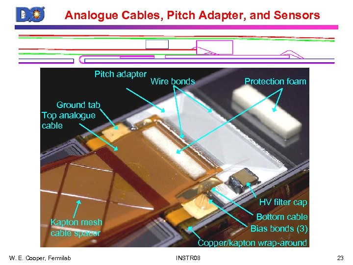 Analogue Cables, Pitch Adapter, and Sensors Pitch adapter Wire bonds Protection foam Ground tab Top analogue cable HV filter cap Bottom cable Bias bonds (3) Kapton mesh cable spacer Copper/kapton wrap-around W. E. Cooper, Fermilab INSTR 08 23
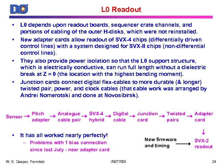 L 0 Readout • • L 0 depends upon readout boards, sequencer crate channels, and portions of cabling of the outer H-disks, which were not reinstalled. New adapter cards allow readout of SVX-4 chips (differentially driven control lines) with a system designed for SVX-II chips (non-differential control lines). They also provide power isolation so that the L 0 support structure, which is electrically conductive, can run full length without a dielectric break at Z = 0 (the location with the highest bending moment). Junction cards connect digital flex-cables to more durable (& longer) twisted pair, power, and clock cables (that cable work was arranged by Andrei Nomerotski and done at Novosibirsk). Sensor • Pitch adapter Analogue cable pair SVX-4 hybrid Digital cable It has all worked nearly perfectly! Twisted pairs New firmware and timing – Problems with 1 bias connection since last July - near adapter card W. E. Cooper, Fermilab Junction card INSTR 08 Adapter card SVX-2 readout 24
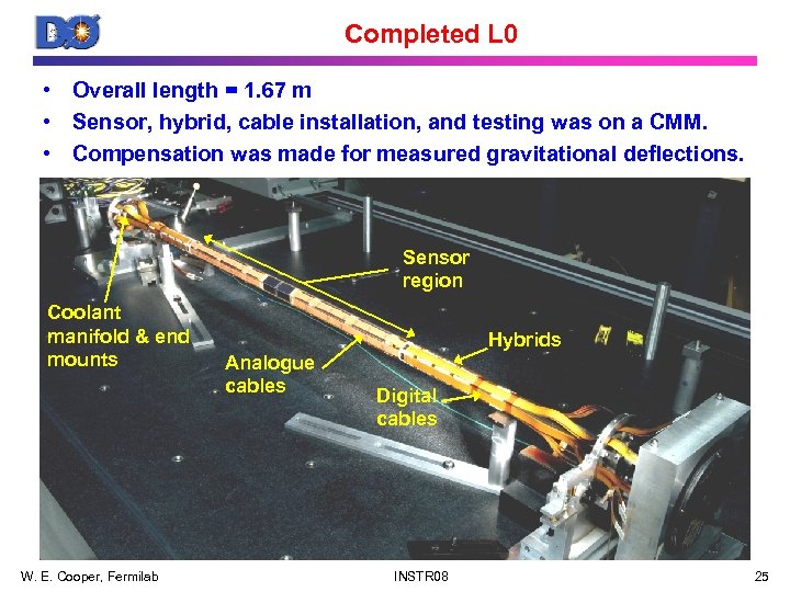 Completed L 0 • Overall length = 1. 67 m • Sensor, hybrid, cable installation, and testing was on a CMM. • Compensation was made for measured gravitational deflections. Sensor region Coolant manifold & end mounts W. E. Cooper, Fermilab Hybrids Analogue cables Digital cables INSTR 08 25
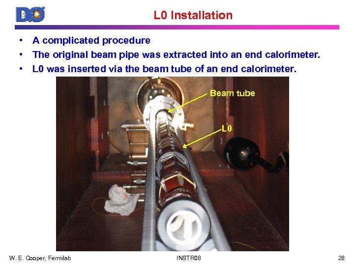 L 0 Installation • A complicated procedure • The original beam pipe was extracted into an end calorimeter. • L 0 was inserted via the beam tube of an end calorimeter. Beam tube L 0 W. E. Cooper, Fermilab INSTR 08 26
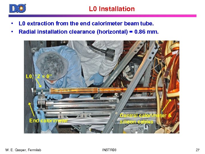 L 0 Installation • L 0 extraction from the end calorimeter beam tube. • Radial installation clearance (horizontal) = 0. 86 mm. L 0, “Z = 0” Central calorimeter & silicon cables End calorimeter W. E. Cooper, Fermilab INSTR 08 27
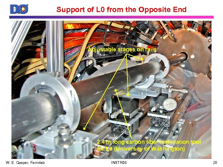 Support of L 0 from the Opposite End Adjustable stages on rails 2. 4 m long carbon fiber installation tool for L 0 (University of Washington) W. E. Cooper, Fermilab INSTR 08 28
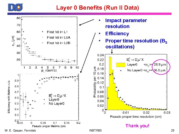 Layer 0 Benefits (Run II Data) • Impact parameter resolution • Efficiency • Proper time resolution (BS oscillations) Thank you! W. E. Cooper, Fermilab INSTR 08 29


