f4c8d14a795df957350863231252f375.ppt
- Количество слайдов: 141

The 8051 Microcontroller hsabaghianb @ kashanu. ac. ir Microprocessors 1 -1
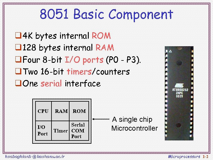
8051 Basic Component q 4 K bytes internal ROM q 128 bytes internal RAM q Four 8 -bit I/O ports (P 0 - P 3). q Two 16 -bit timers/counters q One serial interface CPU I/O Port RAM ROM Serial Timer COM Port hsabaghianb @ kashanu. ac. ir A single chip Microcontroller Microprocessors 1 -2
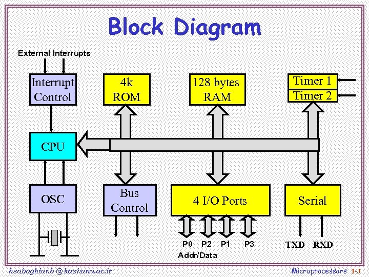
Block Diagram External Interrupts Interrupt Control Timer 1 Timer 2 4 k ROM 128 bytes RAM Bus Control 4 I/O Ports CPU OSC P 0 P 2 P 1 Addr/Data hsabaghianb @ kashanu. ac. ir P 3 Serial TXD RXD Microprocessors 1 -3
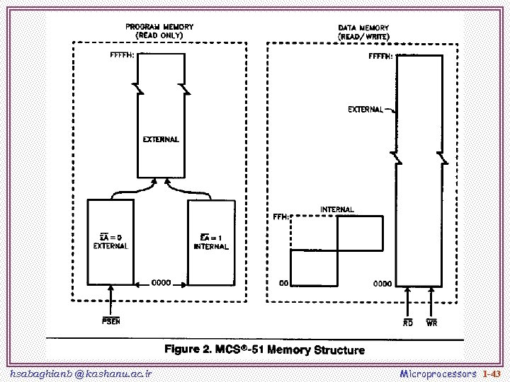
Other 8051 featurs q only 1 On chip oscillator (external crystal) q 6 interrupt sources (2 external , 3 internal, Reset) q 64 K external code (program) memory(only read)PSEN q 64 K external data memory(can be read and write) by RD, WR q Code memory is selectable by EA (internal or external) q We may have External memory as data and code hsabaghianb @ kashanu. ac. ir Microprocessors 1 -4
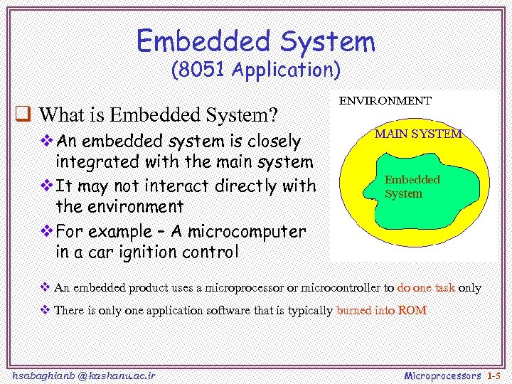
Embedded System (8051 Application) q What is Embedded System? v. An embedded system is closely integrated with the main system v. It may not interact directly with the environment v. For example – A microcomputer in a car ignition control v An embedded product uses a microprocessor or microcontroller to do one task only v There is only one application software that is typically burned into ROM hsabaghianb @ kashanu. ac. ir Microprocessors 1 -5
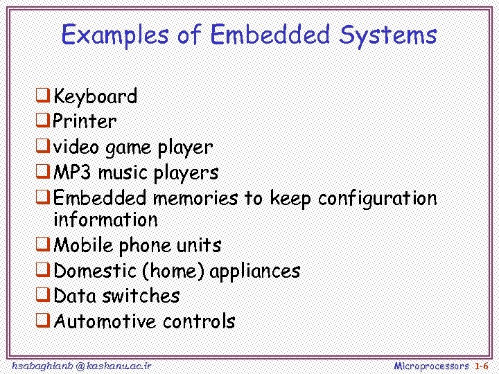
Examples of Embedded Systems q Keyboard q Printer q video game player q MP 3 music players q Embedded memories to keep configuration information q Mobile phone units q Domestic (home) appliances q Data switches q Automotive controls hsabaghianb @ kashanu. ac. ir Microprocessors 1 -6
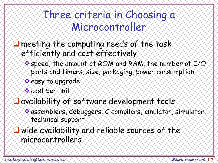
Three criteria in Choosing a Microcontroller q meeting the computing needs of the task efficiently and cost effectively v speed, the amount of ROM and RAM, the number of I/O ports and timers, size, packaging, power consumption v easy to upgrade v cost per unit q availability of software development tools v assemblers, debuggers, C compilers, emulator, simulator, technical support q wide availability and reliable sources of the microcontrollers hsabaghianb @ kashanu. ac. ir Microprocessors 1 -7
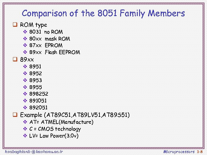
Comparison of the 8051 Family Members q ROM type v v 8031 80 xx 87 xx 89 xx q 89 xx v v v v no ROM mask ROM EPROM Flash EEPROM 8951 8952 8953 8955 898252 891051 892051 q Example (AT 89 C 51, AT 89 LV 51, AT 89 S 51) v AT= ATMEL(Manufacture) v C = CMOS technology v LV= Low Power(3. 0 v) hsabaghianb @ kashanu. ac. ir Microprocessors 1 -8
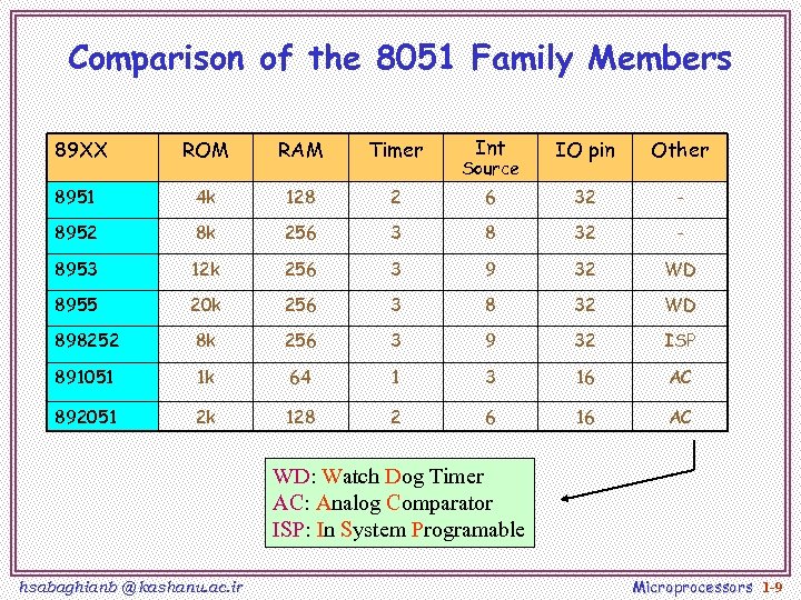
Comparison of the 8051 Family Members Int IO pin Other 2 6 32 - 256 3 8 32 - 12 k 256 3 9 32 WD 20 k 256 3 8 32 WD 898252 8 k 256 3 9 32 ISP 891051 1 k 64 1 3 16 AC 892051 2 k 128 2 6 16 AC 89 XX ROM RAM Timer 8951 4 k 128 8952 8 k 8953 8955 Source WD: Watch Dog Timer AC: Analog Comparator ISP: In System Programable hsabaghianb @ kashanu. ac. ir Microprocessors 1 -9
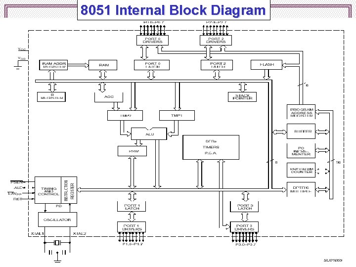
8051 Internal Block Diagram hsabaghianb @ kashanu. ac. ir Microprocessors 1 -10
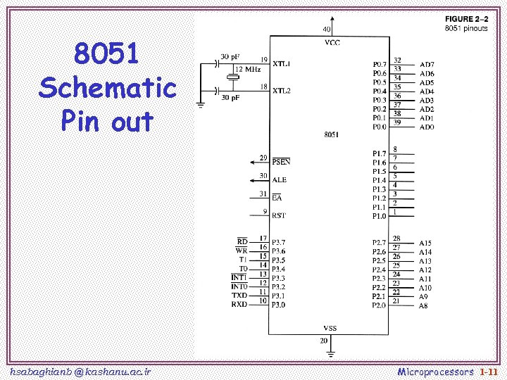
8051 Schematic Pin out hsabaghianb @ kashanu. ac. ir Microprocessors 1 -11
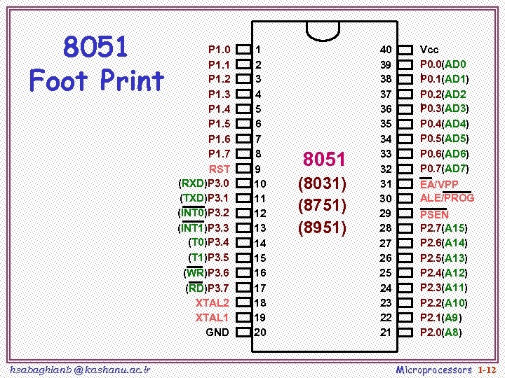
8051 Foot Print P 1. 0 P 1. 1 P 1. 2 P 1. 3 P 1. 4 P 1. 5 P 1. 6 P 1. 7 RST (RXD)P 3. 0 (TXD)P 3. 1 (INT 0)P 3. 2 (INT 1)P 3. 3 (T 0)P 3. 4 (T 1)P 3. 5 (WR)P 3. 6 (RD)P 3. 7 XTAL 2 XTAL 1 GND hsabaghianb @ kashanu. ac. ir 1 2 3 4 5 6 7 8 9 10 11 12 13 14 15 16 17 18 19 20 8051 (8031) (8751) (8951) 40 39 38 37 36 35 34 33 32 31 30 29 28 27 26 25 24 23 22 21 Vcc P 0. 0(AD 0 ) 0. 1(AD 1) P P 0. 2(AD 2 ) 0. 3(AD 3) P P 0. 4(AD 4) P 0. 5(AD 5) P 0. 6(AD 6) P 0. 7(AD 7) EA/VPP ALE/PROG PSEN P 2. 7(A 15) P 2. 6(A 14) P 2. 5(A 13) P 2. 4(A 12) P 2. 3(A 11) P 2. 2(A 10) P 2. 1(A 9) P 2. 0(A 8) Microprocessors 1 -12
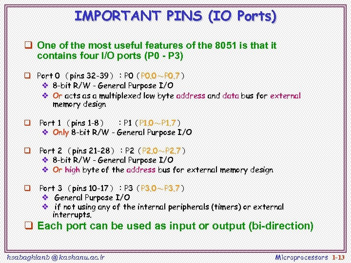
IMPORTANT PINS (IO Ports) q One of the most useful features of the 8051 is that it contains four I/O ports (P 0 - P 3) q Port 0 (pins 32 -39):P 0(P 0. 0~P 0. 7) v 8 -bit R/W - General Purpose I/O v Or acts as a multiplexed low byte address and data bus for external memory design q Port 1 (pins 1 -8) :P 1(P 1. 0~P 1. 7) v Only 8 -bit R/W - General Purpose I/O q Port 2 (pins 21 -28):P 2(P 2. 0~P 2. 7) v 8 -bit R/W - General Purpose I/O v Or high byte of the address bus for external memory design q Port 3 (pins 10 -17):P 3(P 3. 0~P 3. 7) v General Purpose I/O v if not using any of the internal peripherals (timers) or external interrupts. q Each port can be used as input or output (bi-direction) hsabaghianb @ kashanu. ac. ir Microprocessors 1 -13
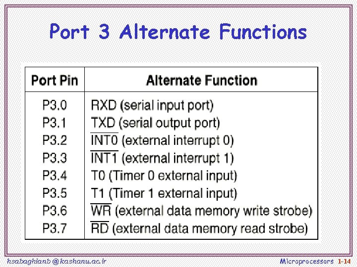
Port 3 Alternate Functions hsabaghianb @ kashanu. ac. ir Microprocessors 1 -14
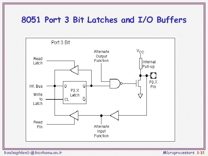
8051 Port 3 Bit Latches and I/O Buffers hsabaghianb @ kashanu. ac. ir Microprocessors 1 -15
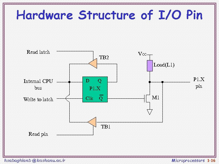
Hardware Structure of I/O Pin Read latch TB 2 Vcc Load(L 1) Internal CPU bus D Write to latch Clk P 1. X pin Q P 1. X Q M 1 TB 1 Read pin hsabaghianb @ kashanu. ac. ir Microprocessors 1 -16
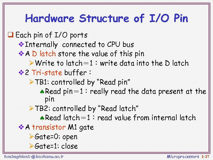
Hardware Structure of I/O Pin q Each pin of I/O ports v. Internally connected to CPU bus v. A D latch store the value of this pin ØWrite to latch= 1:write data into the D latch v 2 Tri-state buffer: ØTB 1: controlled by “Read pin” ªRead pin= 1:really read the data present at the pin ØTB 2: controlled by “Read latch” ªRead latch= 1:read value from internal latch v. A transistor M 1 gate ØGate=0: open ØGate=1: close hsabaghianb @ kashanu. ac. ir Microprocessors 1 -17
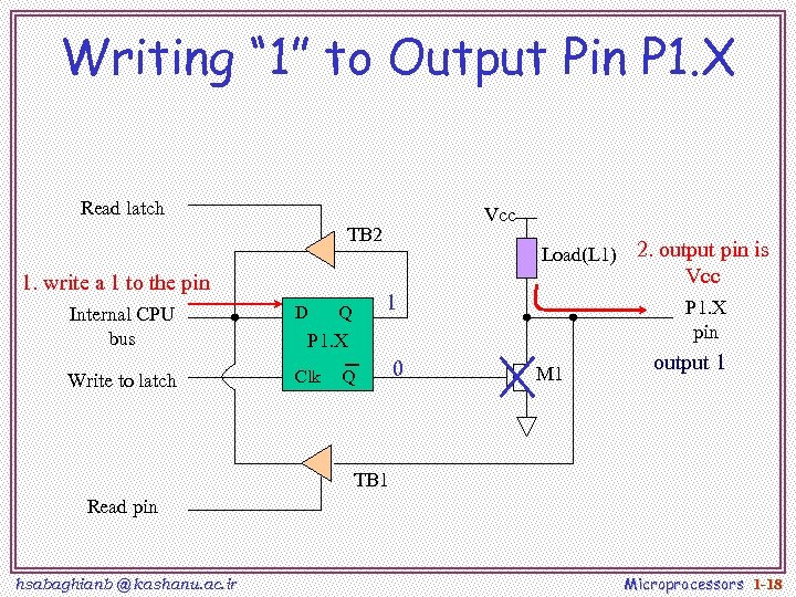
Writing “ 1” to Output Pin P 1. X Read latch Vcc TB 2 Load(L 1) 2. output pin is Vcc 1. write a 1 to the pin Internal CPU bus D Write to latch Clk 1 Q P 1. X pin P 1. X Q 0 M 1 output 1 TB 1 Read pin hsabaghianb @ kashanu. ac. ir Microprocessors 1 -18
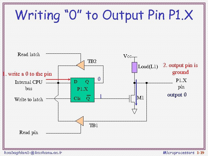
Writing “ 0” to Output Pin P 1. X Read latch Vcc TB 2 Load(L 1) 2. output pin is ground 1. write a 0 to the pin Internal CPU bus D Write to latch Clk 0 Q P 1. X pin P 1. X Q 1 M 1 output 0 TB 1 Read pin hsabaghianb @ kashanu. ac. ir Microprocessors 1 -19
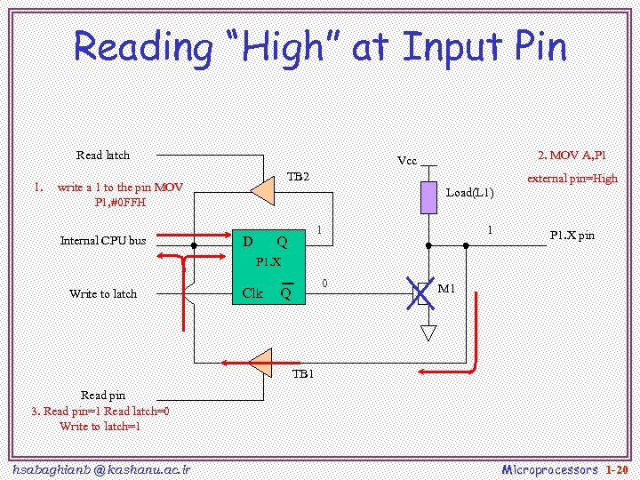
Reading “High” at Input Pin Read latch 1. TB 2 write a 1 to the pin MOV P 1, #0 FFH Internal CPU bus 2. MOV A, P 1 Vcc external pin=High Load(L 1) D 1 Q 1 P 1. X pin P 1. X Write to latch Clk 0 Q M 1 TB 1 Read pin 3. Read pin=1 Read latch=0 Write to latch=1 hsabaghianb @ kashanu. ac. ir Microprocessors 1 -20
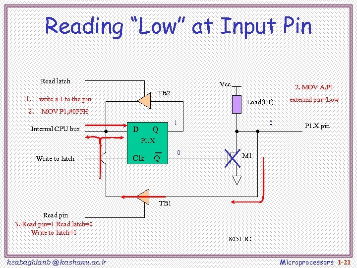
Reading “Low” at Input Pin Read latch 1. Vcc write a 1 to the pin 2. MOV A, P 1 TB 2 Load(L 1) external pin=Low MOV P 1, #0 FFH Internal CPU bus D 1 Q 0 P 1. X pin P 1. X Write to latch Clk Q 0 M 1 TB 1 Read pin 3. Read pin=1 Read latch=0 Write to latch=1 hsabaghianb @ kashanu. ac. ir 8051 IC Microprocessors 1 -21
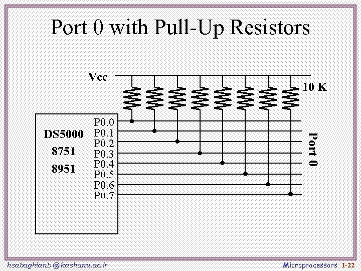
Port 0 with Pull-Up Resistors Vcc hsabaghianb @ kashanu. ac. ir Port 0 P 0. 0 DS 5000 P 0. 1 P 0. 2 8751 P 0. 3 P 0. 4 8951 P 0. 5 P 0. 6 P 0. 7 10 K Microprocessors 1 -22
IMPORTANT PINS q. PSEN (out): Program Store Enable, the read signal for external program memory (active low). q ALE (out): Address Latch Enable, to latch address outputs at Port 0 and Port 2 q EA (in): External Access Enable, active low to access external program memory locations 0 to 4 K q RXD, TXD: UART pins for serial I/O on Port 3 q XTAL 1 & XTAL 2: Crystal inputs for internal oscillator. hsabaghianb @ kashanu. ac. ir Microprocessors 1 -23
Pins of 8051 q Vcc(pin 40): v. Vcc provides supply voltage to the chip. v. The voltage source is +5 V. q GND(pin 20):ground q XTAL 1 and XTAL 2(pins 19, 18): v. These 2 pins provide external clock. v. Way 1:using a quartz crystal oscillator v. Way 2:using a TTL oscillator v. Example 4 -1 shows the relationship between XTAL and the machine cycle. hsabaghianb @ kashanu. ac. ir Microprocessors 1 -24
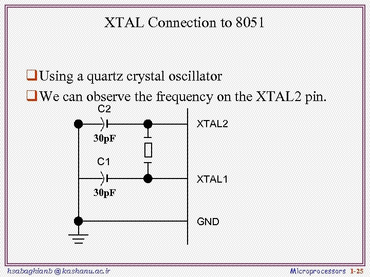
XTAL Connection to 8051 q Using a quartz crystal oscillator q We can observe the frequency on the XTAL 2 pin. C 2 XTAL 2 30 p. F C 1 XTAL 1 30 p. F GND hsabaghianb @ kashanu. ac. ir Microprocessors 1 -25
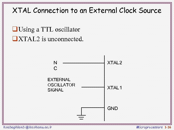
XTAL Connection to an External Clock Source q Using a TTL oscillator q XTAL 2 is unconnected. N C EXTERNAL OSCILLATOR SIGNAL XTAL 2 XTAL 1 GND hsabaghianb @ kashanu. ac. ir Microprocessors 1 -26
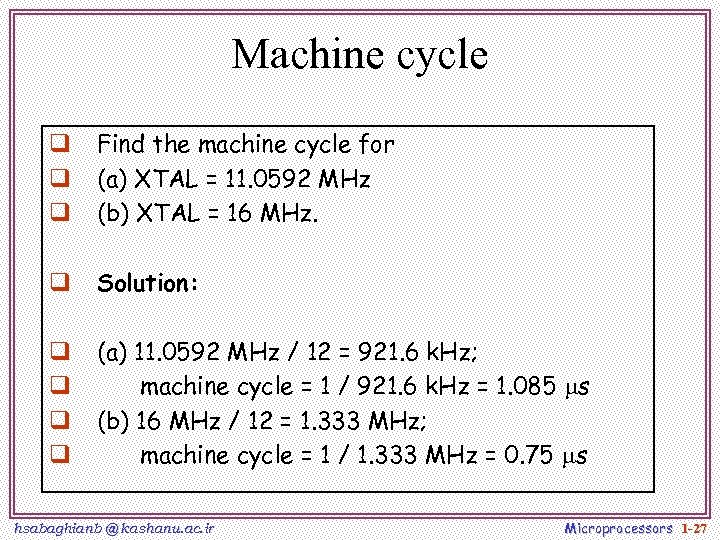
Machine cycle q q q Find the machine cycle for (a) XTAL = 11. 0592 MHz (b) XTAL = 16 MHz. q Solution: q q (a) 11. 0592 MHz / 12 = 921. 6 k. Hz; machine cycle = 1 / 921. 6 k. Hz = 1. 085 s (b) 16 MHz / 12 = 1. 333 MHz; machine cycle = 1 / 1. 333 MHz = 0. 75 s hsabaghianb @ kashanu. ac. ir Microprocessors 1 -27
Pins of 8051 q RST(pin 9):reset v input pin and active high(normally low). ØThe high pulse must be high at least 2 machine cycles. v power-on reset. ØUpon applying a high pulse to RST, the microcontroller will reset and all values in registers will be lost. ØReset values of some 8051 registers v power-on reset circuit hsabaghianb @ kashanu. ac. ir Microprocessors 1 -28
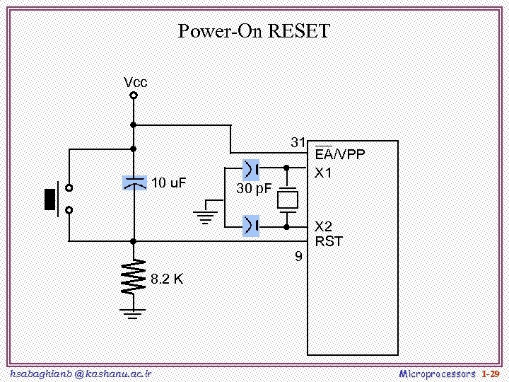
Power-On RESET Vcc 31 10 u. F 30 p. F 9 EA/VPP X 1 X 2 RST 8. 2 K hsabaghianb @ kashanu. ac. ir Microprocessors 1 -29
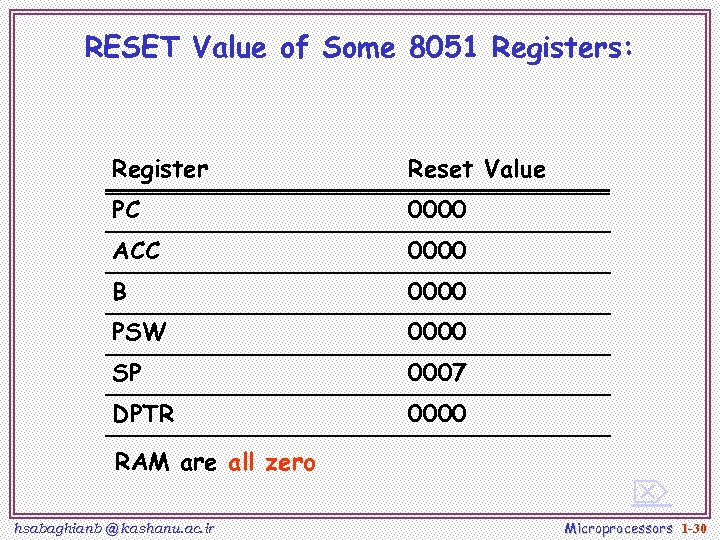
RESET Value of Some 8051 Registers: Register Reset Value PC 0000 ACC 0000 B 0000 PSW 0000 SP 0007 DPTR 0000 RAM are all zero hsabaghianb @ kashanu. ac. ir Microprocessors 1 -30
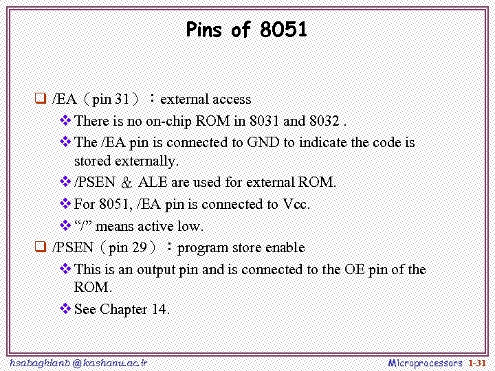
Pins of 8051 q /EA(pin 31):external access v There is no on-chip ROM in 8031 and 8032. v The /EA pin is connected to GND to indicate the code is stored externally. v /PSEN & ALE are used for external ROM. v For 8051, /EA pin is connected to Vcc. v “/” means active low. q /PSEN(pin 29):program store enable v This is an output pin and is connected to the OE pin of the ROM. v See Chapter 14. hsabaghianb @ kashanu. ac. ir Microprocessors 1 -31
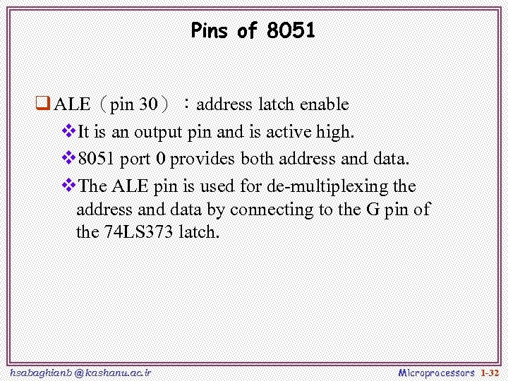
Pins of 8051 q ALE(pin 30):address latch enable v. It is an output pin and is active high. v 8051 port 0 provides both address and data. v. The ALE pin is used for de-multiplexing the address and data by connecting to the G pin of the 74 LS 373 latch. hsabaghianb @ kashanu. ac. ir Microprocessors 1 -32
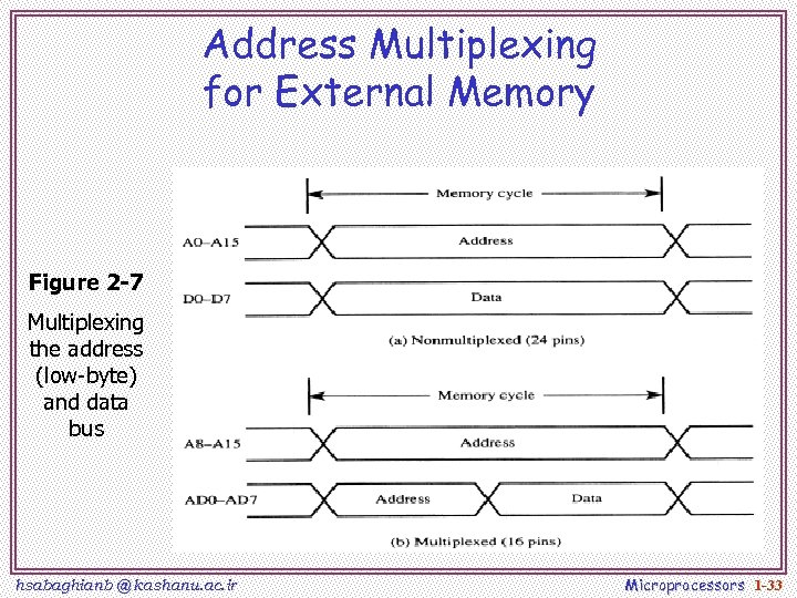
Address Multiplexing for External Memory Figure 2 -7 Multiplexing the address (low-byte) and data bus hsabaghianb @ kashanu. ac. ir Microprocessors 1 -33
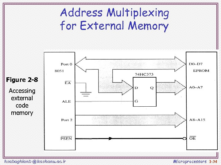
Address Multiplexing for External Memory Figure 2 -8 Accessing external code memory hsabaghianb @ kashanu. ac. ir Microprocessors 1 -34
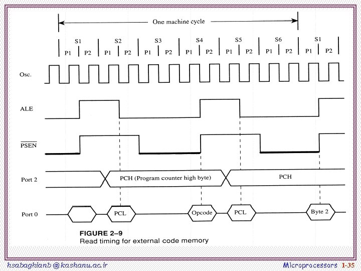
hsabaghianb @ kashanu. ac. ir Microprocessors 1 -35
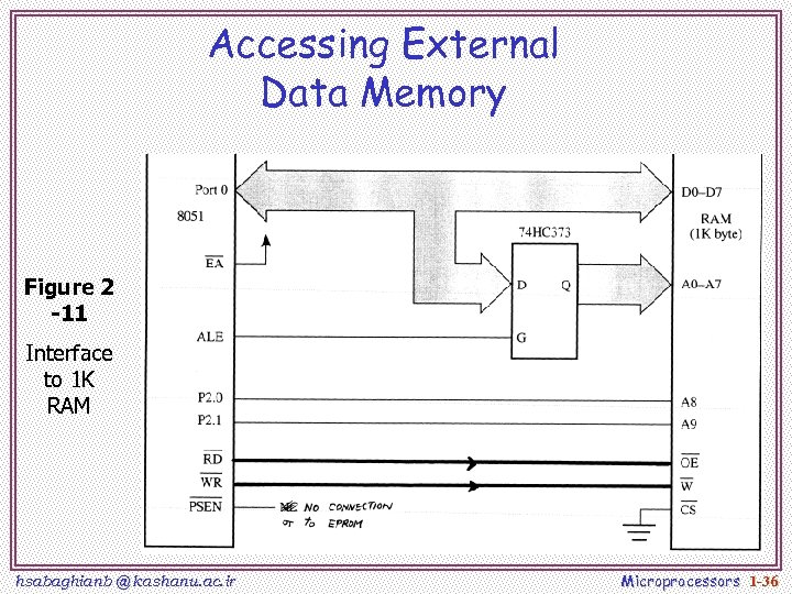
Accessing External Data Memory Figure 2 -11 Interface to 1 K RAM hsabaghianb @ kashanu. ac. ir Microprocessors 1 -36
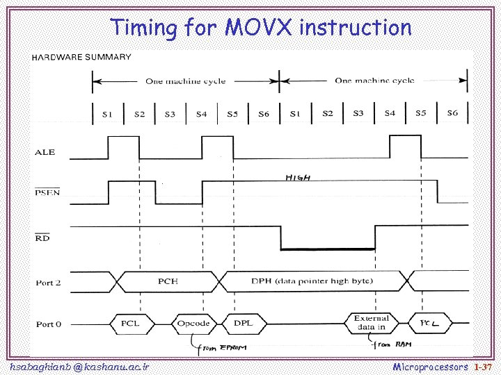
Timing for MOVX instruction hsabaghianb @ kashanu. ac. ir Microprocessors 1 -37
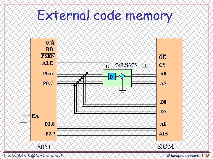
External code memory WR RD PSEN ALE P 0. 0 P 0. 7 74 LS 373 G D OE CS A 0 A 7 D 0 D 7 EA P 2. 0 A 8 P 2. 7 A 15 8051 hsabaghianb @ kashanu. ac. ir ROM Microprocessors 1 -38
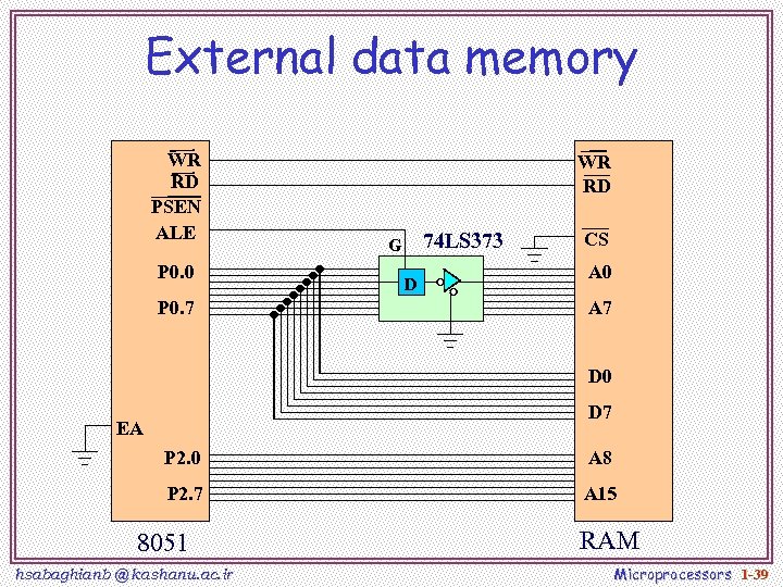
External data memory WR RD PSEN ALE P 0. 0 P 0. 7 WR RD 74 LS 373 G D CS A 0 A 7 D 0 D 7 EA P 2. 0 A 8 P 2. 7 A 15 8051 hsabaghianb @ kashanu. ac. ir RAM Microprocessors 1 -39
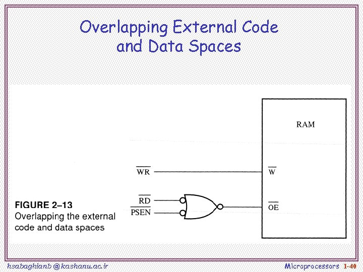
Overlapping External Code and Data Spaces hsabaghianb @ kashanu. ac. ir Microprocessors 1 -40
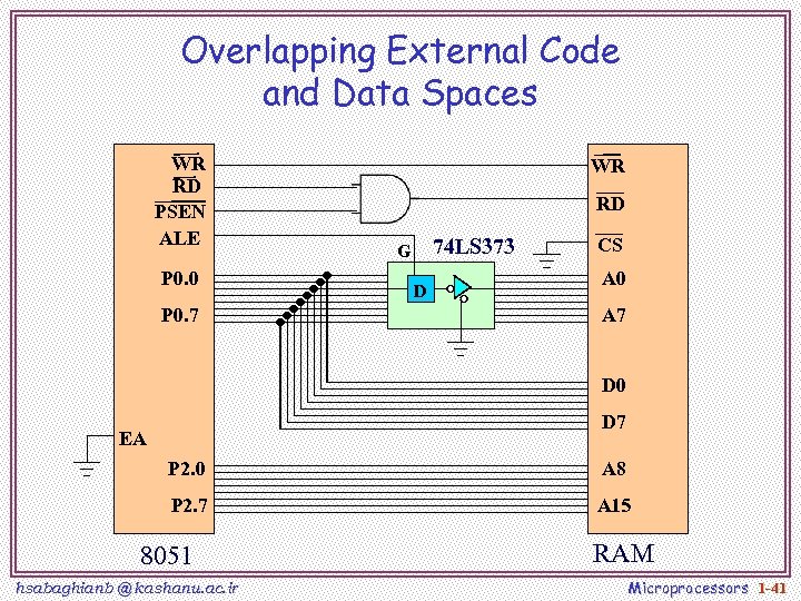
Overlapping External Code and Data Spaces WR RD PSEN ALE P 0. 0 P 0. 7 WR RD 74 LS 373 G D CS A 0 A 7 D 0 D 7 EA P 2. 0 A 8 P 2. 7 A 15 8051 hsabaghianb @ kashanu. ac. ir RAM Microprocessors 1 -41
Overlapping External Code and Data Spaces q. Allows the RAM to be v written as data memory, and v read as data memory as well as code memory. q. This allows a program to be vdownloaded from outside into the RAM as data, and v executed from RAM as code. hsabaghianb @ kashanu. ac. ir Microprocessors 1 -42
hsabaghianb @ kashanu. ac. ir Microprocessors 1 -43
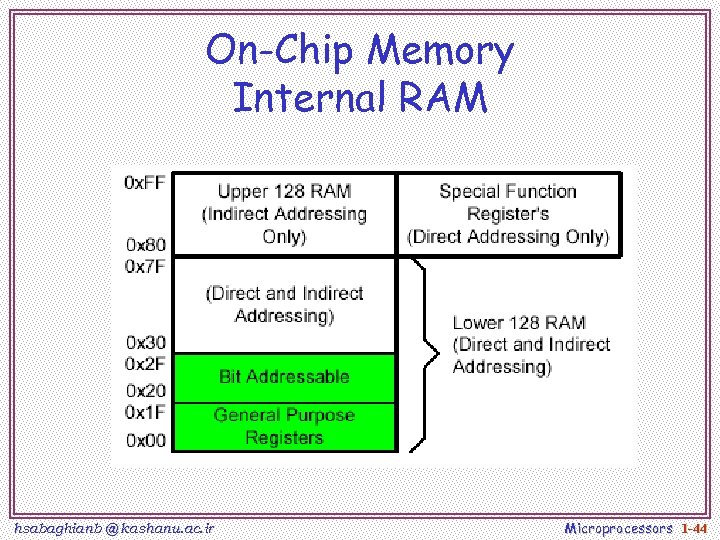
On-Chip Memory Internal RAM hsabaghianb @ kashanu. ac. ir Microprocessors 1 -44
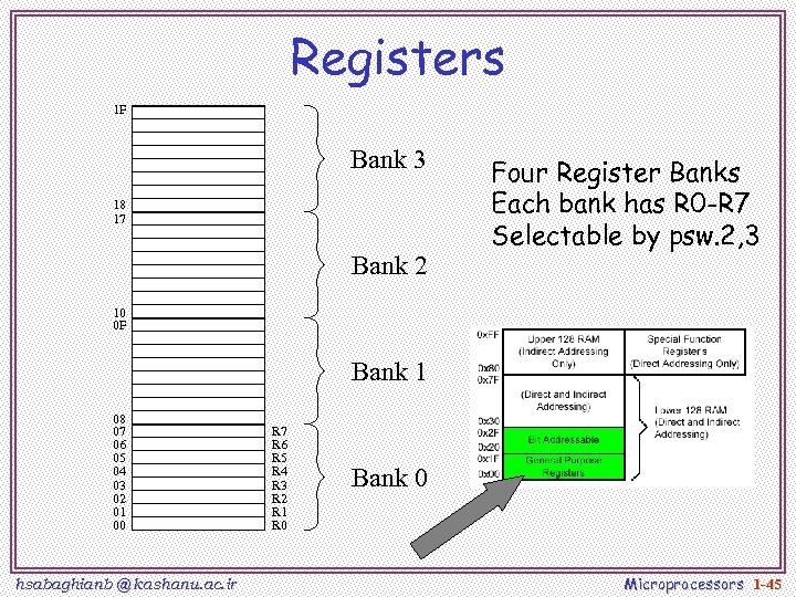
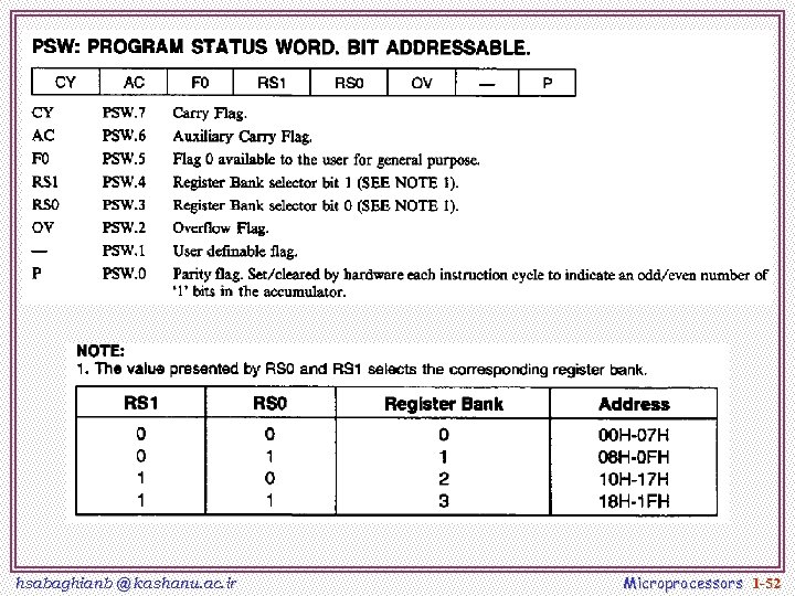
Registers 1 F Bank 3 18 17 Bank 2 Four Register Banks Each bank has R 0 -R 7 Selectable by psw. 2, 3 10 0 F Bank 1 08 07 06 05 04 03 02 01 00 hsabaghianb @ kashanu. ac. ir R 7 R 6 R 5 R 4 R 3 R 2 R 1 R 0 Bank 0 Microprocessors 1 -45
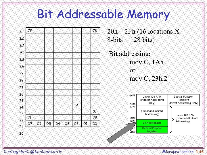
Bit Addressable Memory 2 F 7 F 78 2 E 2 D 20 h – 2 Fh (16 locations X 8 -bits = 128 bits) Bit addressing: mov C, 1 Ah or mov C, 23 h. 2 2 C 2 B 2 A 29 28 27 26 25 1 A 24 23 22 21 10 0 F 07 08 06 05 04 03 02 01 00 20 hsabaghianb @ kashanu. ac. ir Microprocessors 1 -46
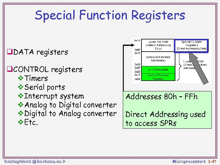
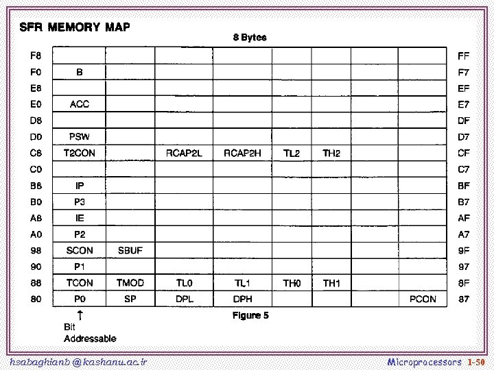
Special Function Registers q. DATA registers q. CONTROL registers v. Timers v. Serial ports v. Interrupt system v. Analog to Digital converter v. Digital to Analog converter v. Etc. hsabaghianb @ kashanu. ac. ir Addresses 80 h – FFh Direct Addressing used to access SPRs Microprocessors 1 -47
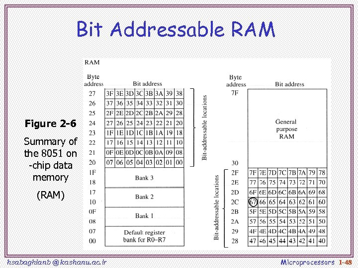
Bit Addressable RAM Figure 2 -6 Summary of the 8051 on -chip data memory (RAM) hsabaghianb @ kashanu. ac. ir Microprocessors 1 -48
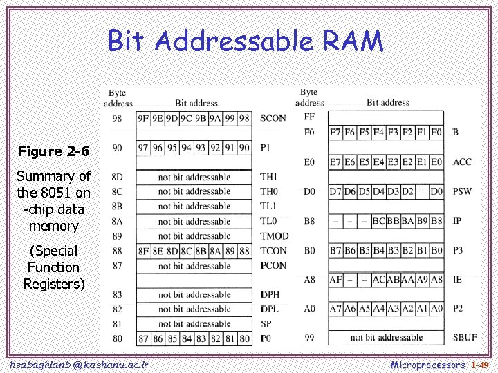
Bit Addressable RAM Figure 2 -6 Summary of the 8051 on -chip data memory (Special Function Registers) hsabaghianb @ kashanu. ac. ir Microprocessors 1 -49
hsabaghianb @ kashanu. ac. ir Microprocessors 1 -50
![Register Banks q Active bank selected by PSW [RS 1, RS 0] bit q Register Banks q Active bank selected by PSW [RS 1, RS 0] bit q](https://present5.com/presentation/f4c8d14a795df957350863231252f375/image-51.jpg)
Register Banks q Active bank selected by PSW [RS 1, RS 0] bit q Permits fast “context switching” in interrupt service routines (ISR). hsabaghianb @ kashanu. ac. ir Microprocessors 1 -51
hsabaghianb @ kashanu. ac. ir Microprocessors 1 -52
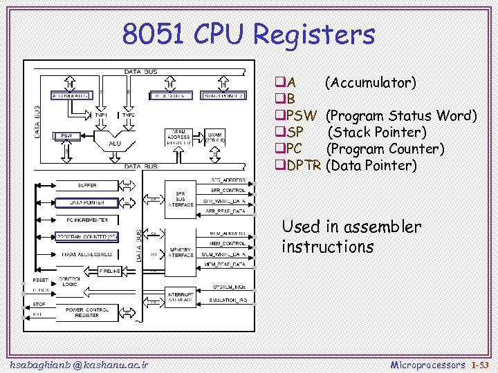
8051 CPU Registers q. A (Accumulator) q. B q. PSW (Program Status Word) q. SP (Stack Pointer) q. PC (Program Counter) q. DPTR (Data Pointer) Used in assembler instructions hsabaghianb @ kashanu. ac. ir Microprocessors 1 -53
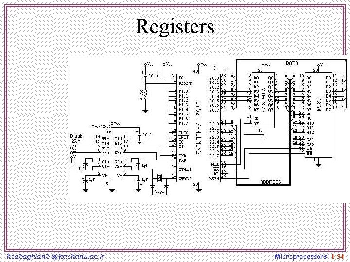
Registers hsabaghianb @ kashanu. ac. ir Microprocessors 1 -54
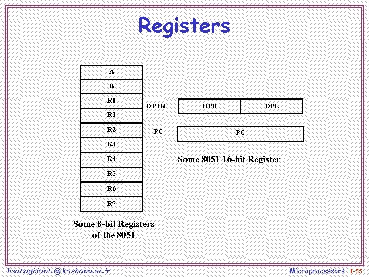
Registers A B R 0 DPTR DPH DPL R 1 R 2 PC PC R 3 R 4 Some 8051 16 -bit Register R 5 R 6 R 7 Some 8 -bit Registers of the 8051 hsabaghianb @ kashanu. ac. ir Microprocessors 1 -55

The 8051 Assembly Language hsabaghianb @ kashanu. ac. ir Microprocessors 1 -56
Overview q Data transfer instructions q Addressing modes q Data processing (arithmetic and logic) q Program flow instructions hsabaghianb @ kashanu. ac. ir Microprocessors 1 -57
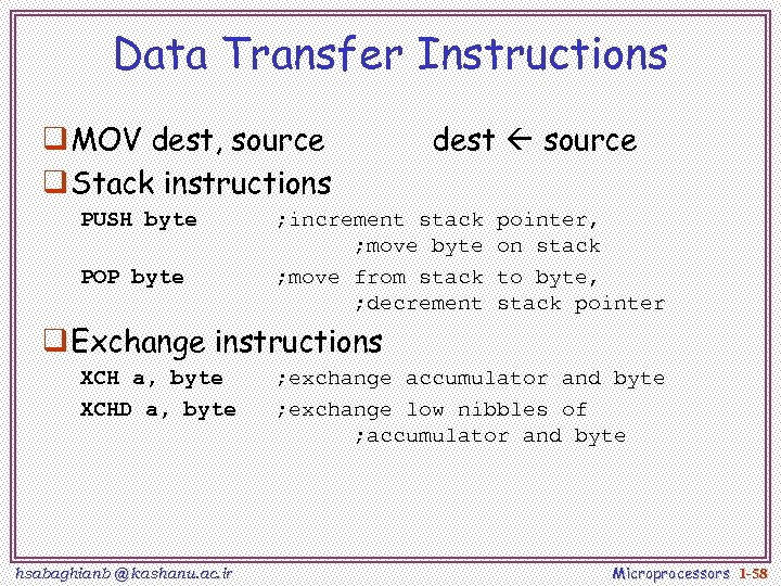
Data Transfer Instructions q MOV dest, source q Stack instructions PUSH byte POP byte dest source ; increment stack ; move byte ; move from stack ; decrement pointer, on stack to byte, stack pointer q Exchange instructions XCH a, byte XCHD a, byte hsabaghianb @ kashanu. ac. ir ; exchange accumulator and byte ; exchange low nibbles of ; accumulator and byte Microprocessors 1 -58
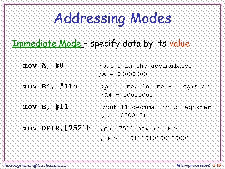
Addressing Modes Immediate Mode – specify data by its value mov A, #0 ; put 0 in the accumulator ; A = 0000 mov R 4, #11 h ; put 11 hex in the R 4 register ; R 4 = 0001 mov B, #11 ; put 11 decimal in b register ; B = 00001011 mov DPTR, #7521 h ; put 7521 hex in DPTR ; DPTR = 0111010100100001 hsabaghianb @ kashanu. ac. ir Microprocessors 1 -59
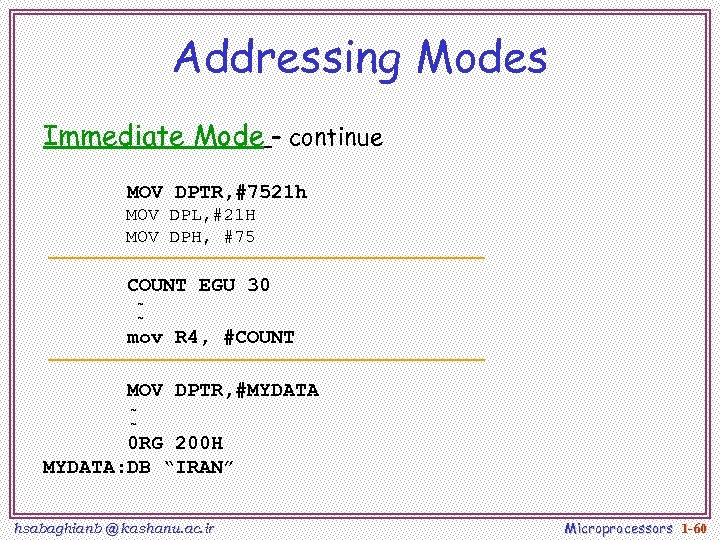
Addressing Modes Immediate Mode – continue MOV DPTR, #7521 h MOV DPL, #21 H MOV DPH, #75 COUNT EGU 30 ~ ~ mov R 4, #COUNT MOV DPTR, #MYDATA ~ ~ 0 RG 200 H MYDATA: DB “IRAN” hsabaghianb @ kashanu. ac. ir Microprocessors 1 -60
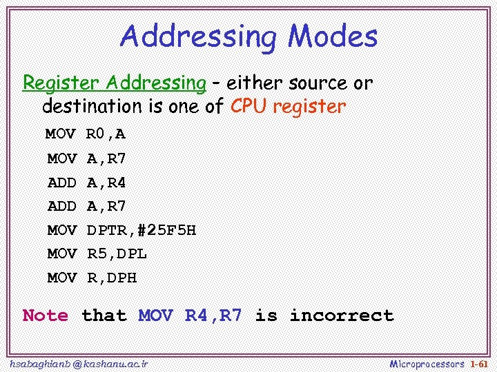
Addressing Modes Register Addressing – either source or destination is one of CPU register MOV ADD MOV MOV R 0, A A, R 7 A, R 4 A, R 7 DPTR, #25 F 5 H R 5, DPL R, DPH Note that MOV R 4, R 7 is incorrect hsabaghianb @ kashanu. ac. ir Microprocessors 1 -61
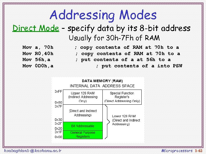
Addressing Modes Direct Mode – specify data by its 8 -bit address Usually for 30 h-7 Fh of RAM Mov Mov a, 70 h R 0, 40 h 56 h, a 0 D 0 h, a hsabaghianb @ kashanu. ac. ir ; copy contents of RAM at 70 h to a ; put contents of a at 56 h to a ; put contents of a into PSW Microprocessors 1 -62
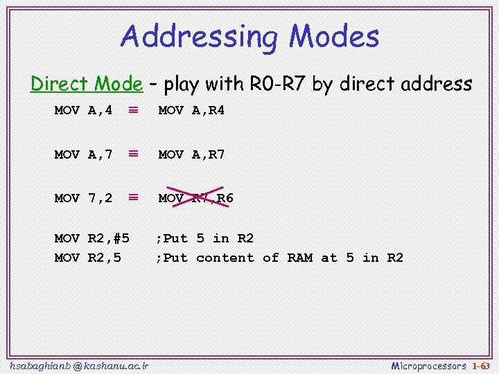
Addressing Modes Direct Mode – play with R 0 -R 7 by direct address MOV A, 4 MOV A, R 4 MOV A, 7 MOV A, R 7 MOV 7, 2 MOV R 7, R 6 MOV R 2, #5 MOV R 2, 5 hsabaghianb @ kashanu. ac. ir ; Put 5 in R 2 ; Put content of RAM at 5 in R 2 Microprocessors 1 -63
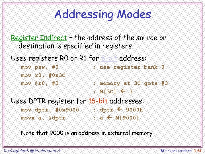
Addressing Modes Register Indirect – the address of the source or destination is specified in registers Uses registers R 0 or R 1 for 8 -bit address: mov psw, #0 mov r 0, #0 x 3 C mov @r 0, #3 ; use register bank 0 ; memory at 3 C gets #3 ; M[3 C] 3 Uses DPTR register for 16 -bit addresses: mov dptr, #0 x 9000 movx a, @dptr ; dptr 9000 h ; a M[9000] Note that 9000 is an address in external memory hsabaghianb @ kashanu. ac. ir Microprocessors 1 -64
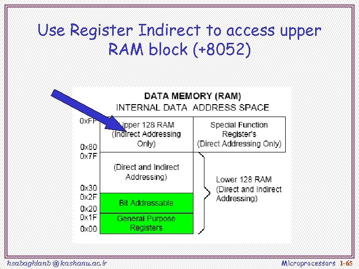
Use Register Indirect to access upper RAM block (+8052) hsabaghianb @ kashanu. ac. ir Microprocessors 1 -65
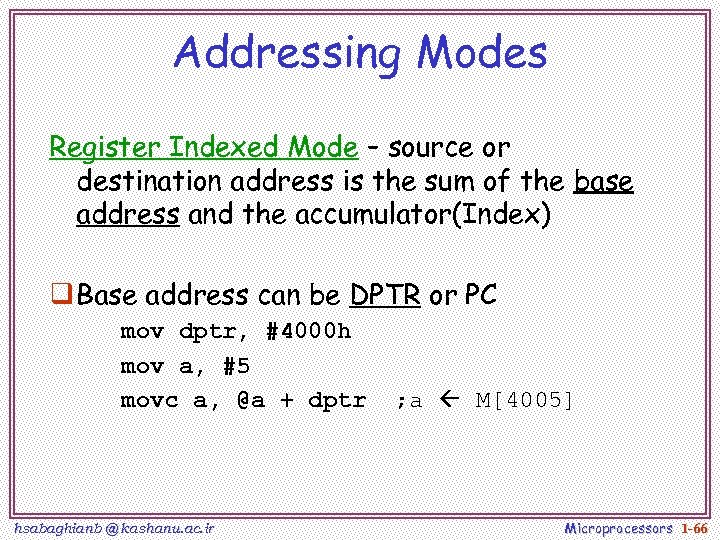
Addressing Modes Register Indexed Mode – source or destination address is the sum of the base address and the accumulator(Index) q Base address can be DPTR or PC mov dptr, #4000 h mov a, #5 movc a, @a + dptr hsabaghianb @ kashanu. ac. ir ; a M[4005] Microprocessors 1 -66
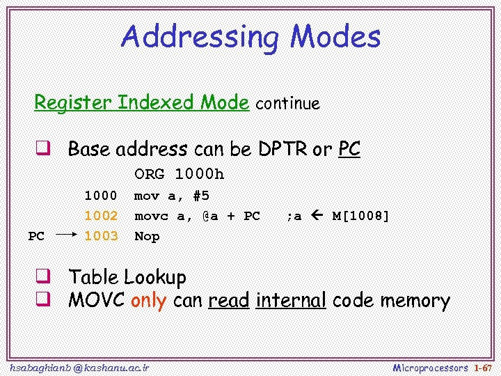
Addressing Modes Register Indexed Mode continue q Base address can be DPTR or PC ORG 1000 h PC 1000 1002 1003 mov a, #5 movc a, @a + PC Nop ; a M[1008] q Table Lookup q MOVC only can read internal code memory hsabaghianb @ kashanu. ac. ir Microprocessors 1 -67
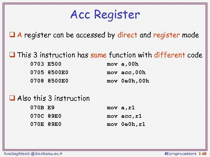
Acc Register q A register can be accessed by direct and register mode q This 3 instruction has same function with different code 0703 E 500 0705 8500 E 0 0708 8500 E 0 mov a, 00 h mov acc, 00 h mov 0 e 0 h, 00 h q Also this 3 instruction 070 B E 9 070 C 89 E 0 070 E 89 E 0 hsabaghianb @ kashanu. ac. ir mov a, r 1 mov acc, r 1 mov 0 e 0 h, r 1 Microprocessors 1 -68
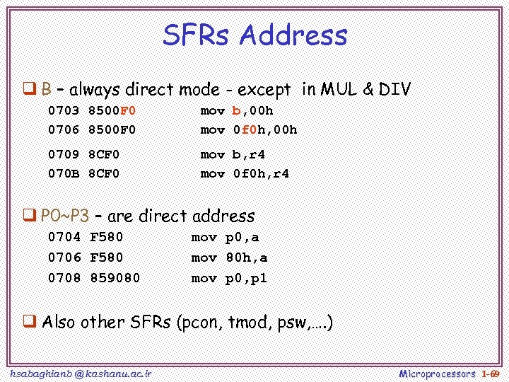
SFRs Address q B – always direct mode - except in MUL & DIV 0703 8500 F 0 0706 8500 F 0 mov b, 00 h mov 0 f 0 h, 00 h 0709 8 CF 0 070 B 8 CF 0 mov b, r 4 mov 0 f 0 h, r 4 q P 0~P 3 – are direct address 0704 F 580 0706 F 580 0708 859080 mov p 0, a mov 80 h, a mov p 0, p 1 q Also other SFRs (pcon, tmod, psw, …. ) hsabaghianb @ kashanu. ac. ir Microprocessors 1 -69
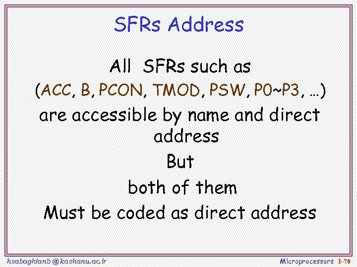
SFRs Address All SFRs such as (ACC, B, PCON, TMOD, PSW, P 0~P 3, …) are accessible by name and direct address But both of them Must be coded as direct address hsabaghianb @ kashanu. ac. ir Microprocessors 1 -70
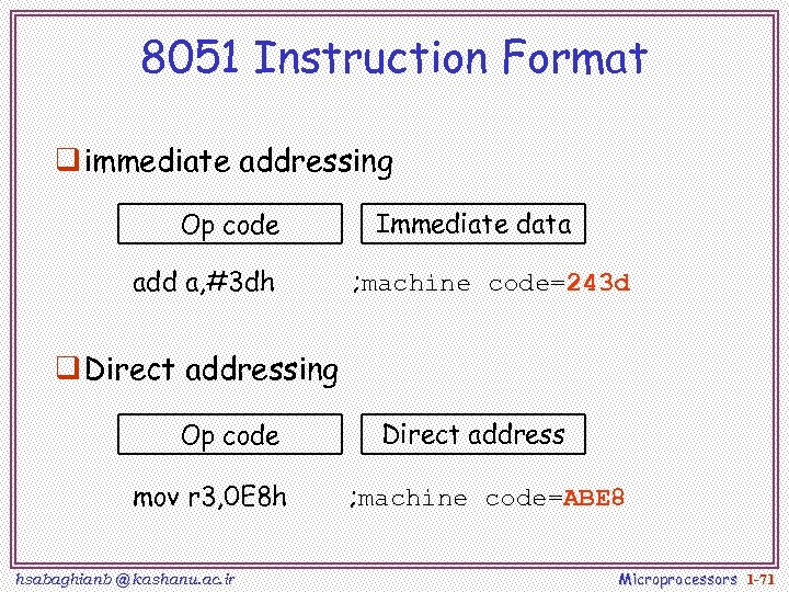
8051 Instruction Format q immediate addressing Op code add a, #3 dh Immediate data ; machine code=243 d q Direct addressing Op code mov r 3, 0 E 8 h hsabaghianb @ kashanu. ac. ir Direct address ; machine code=ABE 8 Microprocessors 1 -71
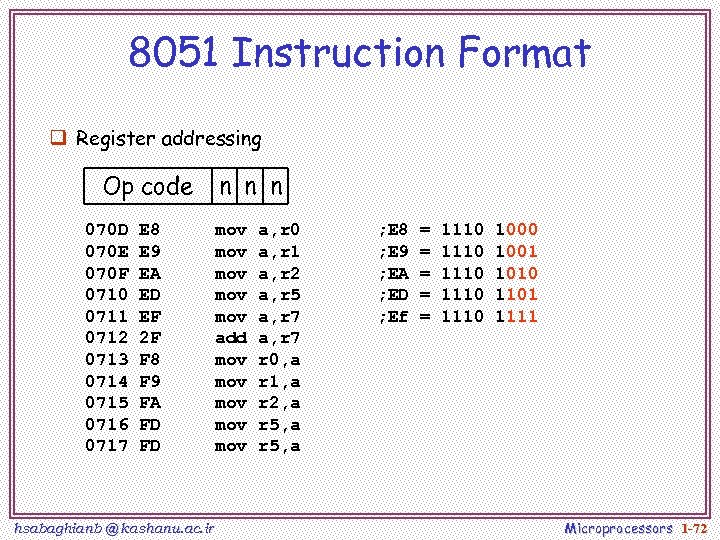
8051 Instruction Format q Register addressing Op code 070 D 070 E 070 F 0710 0711 0712 0713 0714 0715 0716 0717 E 8 E 9 EA ED EF 2 F F 8 F 9 FA FD FD hsabaghianb @ kashanu. ac. ir n n n mov mov mov add mov mov mov a, r 0 a, r 1 a, r 2 a, r 5 a, r 7 r 0, a r 1, a r 2, a r 5, a ; E 8 ; E 9 ; EA ; ED ; Ef = = = 1110 1110 1001 1010 1101 1111 Microprocessors 1 -72
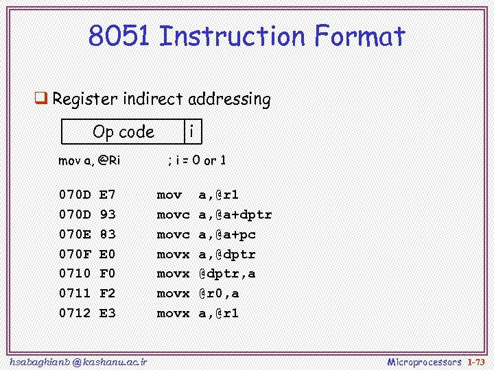
8051 Instruction Format q Register indirect addressing Op code mov a, @Ri 070 D 070 E 070 F 0710 0711 0712 E 7 93 83 E 0 F 2 E 3 hsabaghianb @ kashanu. ac. ir i ; i = 0 or 1 movc movx movx a, @r 1 a, @a+dptr a, @a+pc a, @dptr, a @r 0, a a, @r 1 Microprocessors 1 -73
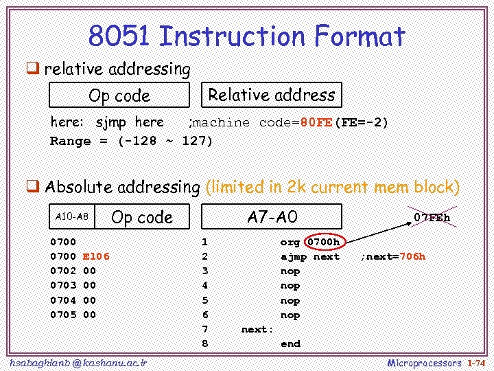
8051 Instruction Format q relative addressing Op code Relative address here: sjmp here ; machine code=80 FE(FE=-2) Range = (-128 ~ 127) q Absolute addressing (limited in 2 k current mem block) A 10 -A 8 0700 0702 0703 0704 0705 Op code E 106 00 00 hsabaghianb @ kashanu. ac. ir A 7 -A 0 1 2 3 4 5 6 7 8 org 0700 h ajmp next nop nop 07 FEh ; next=706 h next: end Microprocessors 1 -74
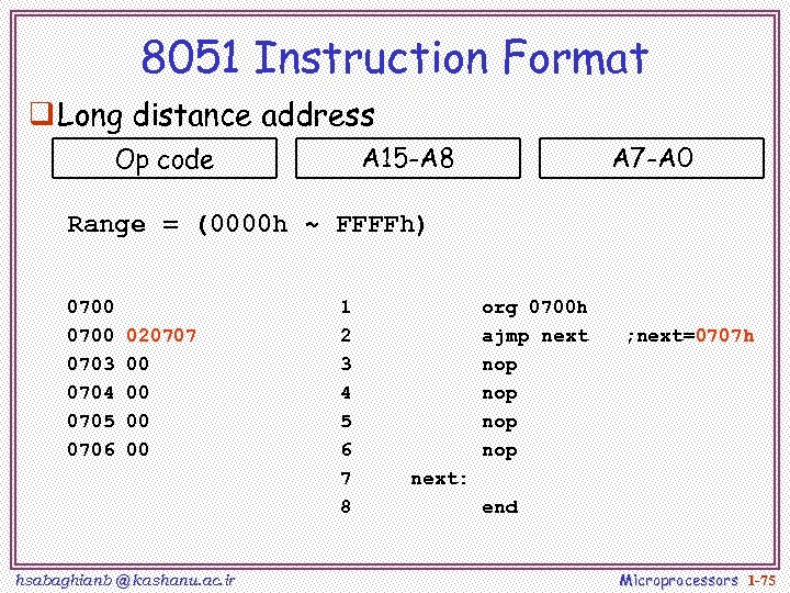
8051 Instruction Format q Long distance address A 15 -A 8 Op code A 7 -A 0 Range = (0000 h ~ FFFFh) 0700 0703 0704 0705 0706 020707 00 00 hsabaghianb @ kashanu. ac. ir 1 2 3 4 5 6 7 8 org 0700 h ajmp next nop nop ; next=0707 h next: end Microprocessors 1 -75
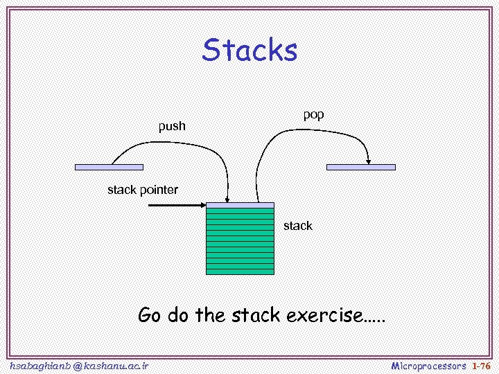
Stacks push pop stack pointer stack Go do the stack exercise…. . hsabaghianb @ kashanu. ac. ir Microprocessors 1 -76
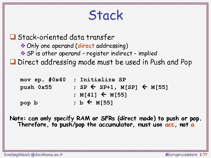
Stack q Stack-oriented data transfer v Only one operand (direct addressing) v SP is other operand – register indirect - implied q Direct addressing mode must be used in Push and Pop mov sp, #0 x 40 push 0 x 55 pop b ; ; Initialize SP SP SP+1, M[SP] M[55] M[41] M[55] b M[55] Note: can only specify RAM or SFRs (direct mode) to push or pop. Therefore, to push/pop the accumulator, must use acc, not a hsabaghianb @ kashanu. ac. ir Microprocessors 1 -77
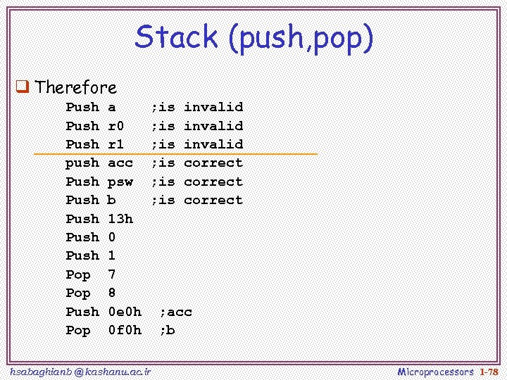
Stack (push, pop) q Therefore Push push Push Pop Push Pop a r 0 r 1 acc psw b 13 h 0 1 7 8 0 e 0 h 0 f 0 h ; is ; is hsabaghianb @ kashanu. ac. ir invalid correct ; acc ; b Microprocessors 1 -78
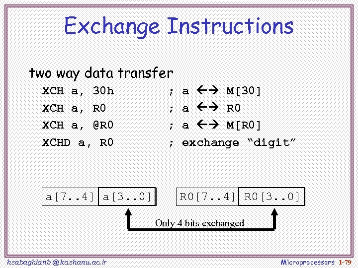
Exchange Instructions two way data transfer XCH a, 30 h XCH a, R 0 XCH a, @R 0 XCHD a, R 0 a[7. . 4] a[3. . 0] ; ; a M[30] a R 0 a M[R 0] exchange “digit” R 0[7. . 4] R 0[3. . 0] Only 4 bits exchanged hsabaghianb @ kashanu. ac. ir Microprocessors 1 -79
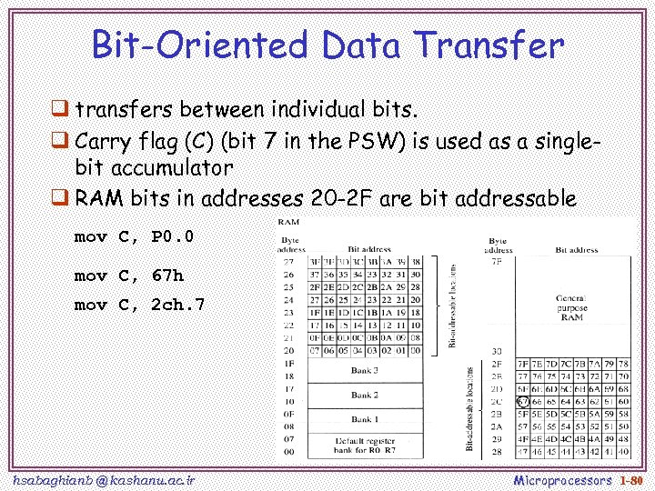
Bit-Oriented Data Transfer q transfers between individual bits. q Carry flag (C) (bit 7 in the PSW) is used as a singlebit accumulator q RAM bits in addresses 20 -2 F are bit addressable mov C, P 0. 0 mov C, 67 h mov C, 2 ch. 7 hsabaghianb @ kashanu. ac. ir Microprocessors 1 -80
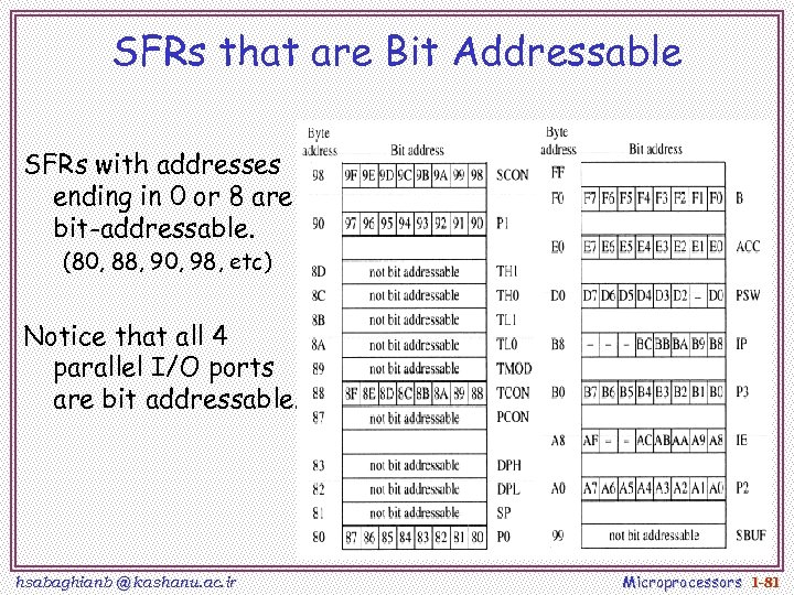
SFRs that are Bit Addressable SFRs with addresses ending in 0 or 8 are bit-addressable. (80, 88, 90, 98, etc) Notice that all 4 parallel I/O ports are bit addressable. hsabaghianb @ kashanu. ac. ir Microprocessors 1 -81
Data Processing Instructions Arithmetic Instructions Logic Instructions hsabaghianb @ kashanu. ac. ir Microprocessors 1 -82
Arithmetic Instructions q Add q Subtract q Increment q Decrement q Multiply q Divide q Decimal adjust hsabaghianb @ kashanu. ac. ir Microprocessors 1 -83
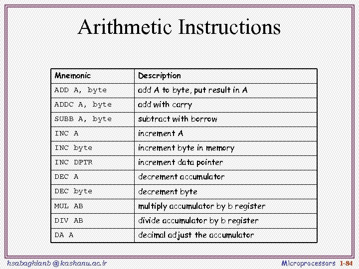
Arithmetic Instructions Mnemonic Description ADD A, byte add A to byte, put result in A ADDC A, byte add with carry SUBB A, byte subtract with borrow INC A increment A INC byte increment byte in memory INC DPTR increment data pointer DEC A decrement accumulator DEC byte decrement byte MUL AB multiply accumulator by b register DIV AB divide accumulator by b register DA A decimal adjust the accumulator hsabaghianb @ kashanu. ac. ir Microprocessors 1 -84
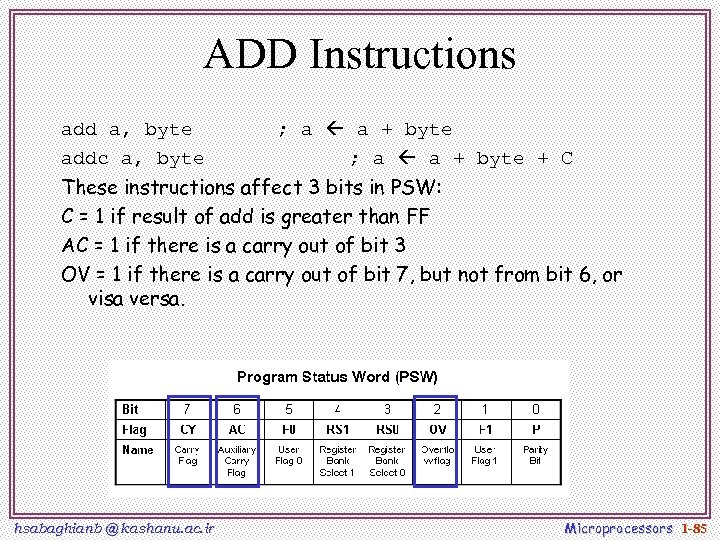
ADD Instructions add a, byte addc a, byte ; a a + byte + C These instructions affect 3 bits in PSW: C = 1 if result of add is greater than FF AC = 1 if there is a carry out of bit 3 OV = 1 if there is a carry out of bit 7, but not from bit 6, or visa versa. hsabaghianb @ kashanu. ac. ir Microprocessors 1 -85
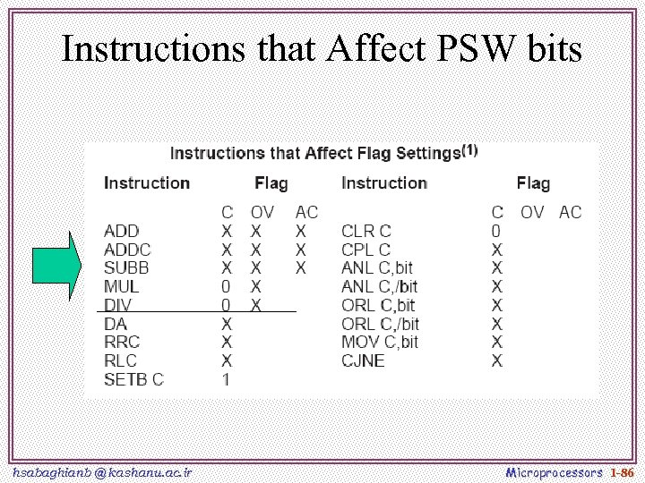
Instructions that Affect PSW bits hsabaghianb @ kashanu. ac. ir Microprocessors 1 -86
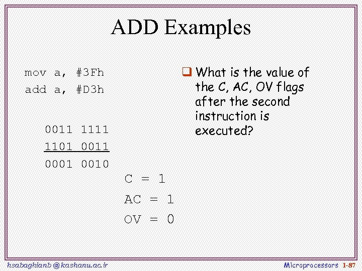
ADD Examples q What is the value of the C, AC, OV flags after the second instruction is executed? mov a, #3 Fh add a, #D 3 h 0011 1101 0011 0001 0010 hsabaghianb @ kashanu. ac. ir C = 1 AC = 1 OV = 0 Microprocessors 1 -87
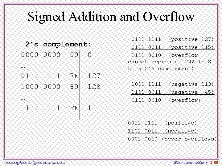
Signed Addition and Overflow 2’s 0000 … 0111 1000 … 1111 complement: 0000 00 0 1111 0000 7 F 127 80 -128 1111 0111 1111 (positive 127) 0111 0011 (positive 115) 1111 0010 (overflow cannot represent 242 in 8 bits 2’s complement) FF -1 1000 1111 1101 0011 0110 0010 (negative 113) (negative 45) (overflow) 0011 1111 (positive) 1101 0011 (negative) 0001 0010 (never overflows) hsabaghianb @ kashanu. ac. ir Microprocessors 1 -88
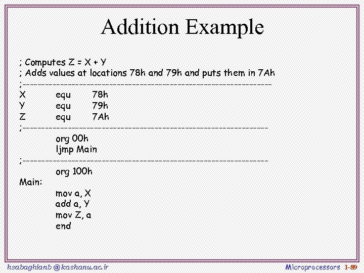
Addition Example ; Computes Z = X + Y ; Adds values at locations 78 h and 79 h and puts them in 7 Ah ; ---------------------------------X equ 78 h Y equ 79 h Z equ 7 Ah ; --------------------------------org 00 h ljmp Main ; --------------------------------org 100 h Main: mov a, X add a, Y mov Z, a end hsabaghianb @ kashanu. ac. ir Microprocessors 1 -89
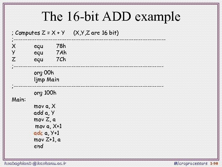
The 16 -bit ADD example ; Computes Z = X + Y (X, Y, Z are 16 bit) ; ---------------------------------X equ 78 h Y equ 7 Ah Z equ 7 Ch ; --------------------------------org 00 h ljmp Main ; --------------------------------org 100 h Main: mov a, X add a, Y mov Z, a mov a, X+1 adc a, Y+1 mov Z+1, a end hsabaghianb @ kashanu. ac. ir Microprocessors 1 -90
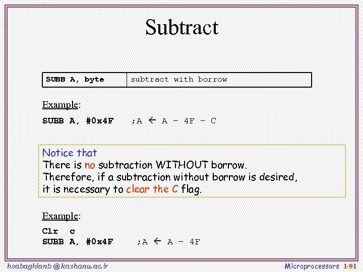
Subtract SUBB A, byte subtract with borrow Example: SUBB A, #0 x 4 F ; A A – 4 F – C Notice that There is no subtraction WITHOUT borrow. Therefore, if a subtraction without borrow is desired, it is necessary to clear the C flag. Example: Clr c SUBB A, #0 x 4 F hsabaghianb @ kashanu. ac. ir ; A A – 4 F Microprocessors 1 -91
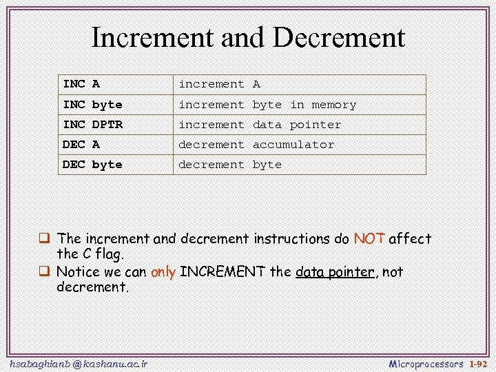
Increment and Decrement INC A increment A INC byte increment byte in memory INC DPTR increment data pointer DEC A decrement accumulator DEC byte decrement byte q The increment and decrement instructions do NOT affect the C flag. q Notice we can only INCREMENT the data pointer, not decrement. hsabaghianb @ kashanu. ac. ir Microprocessors 1 -92
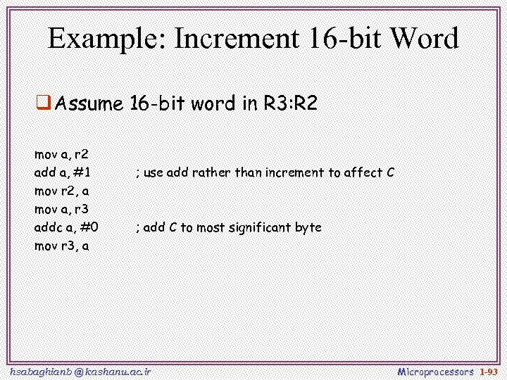
Example: Increment 16 -bit Word q Assume 16 -bit word in R 3: R 2 mov a, r 2 add a, #1 mov r 2, a mov a, r 3 addc a, #0 mov r 3, a ; use add rather than increment to affect C ; add C to most significant byte hsabaghianb @ kashanu. ac. ir Microprocessors 1 -93
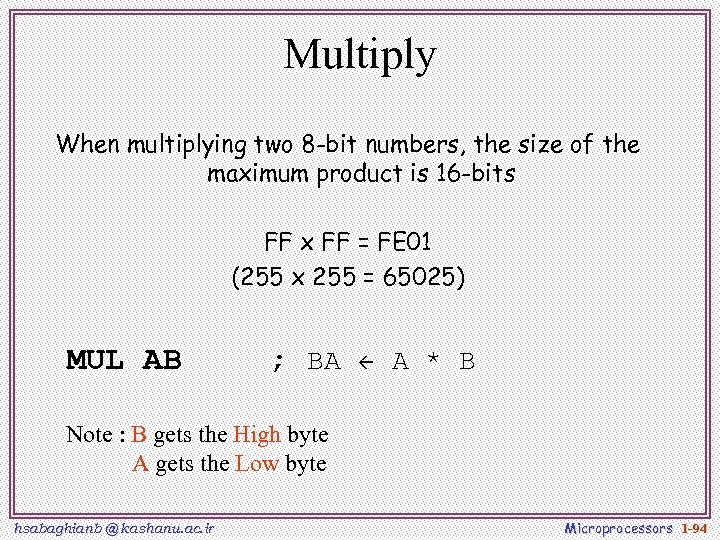
Multiply When multiplying two 8 -bit numbers, the size of the maximum product is 16 -bits FF x FF = FE 01 (255 x 255 = 65025) MUL AB ; BA A * B Note : B gets the High byte A gets the Low byte hsabaghianb @ kashanu. ac. ir Microprocessors 1 -94
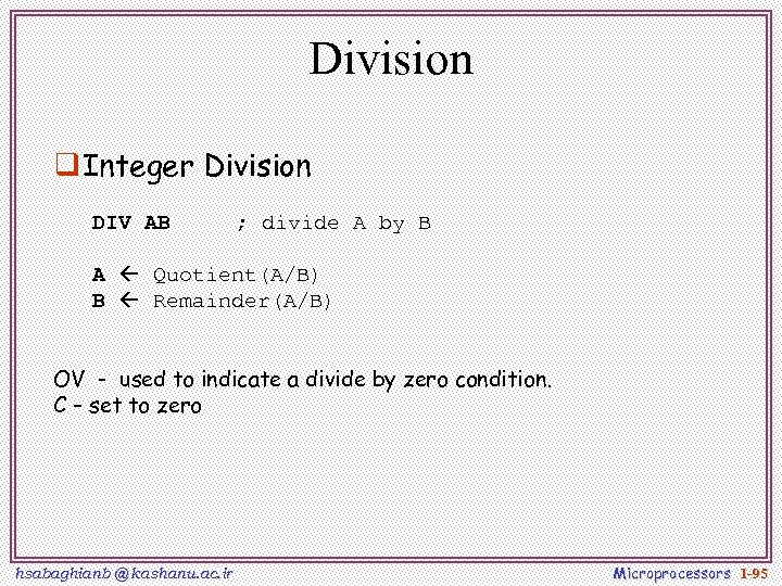
Division q Integer Division DIV AB ; divide A by B A Quotient(A/B) B Remainder(A/B) OV - used to indicate a divide by zero condition. C – set to zero hsabaghianb @ kashanu. ac. ir Microprocessors 1 -95
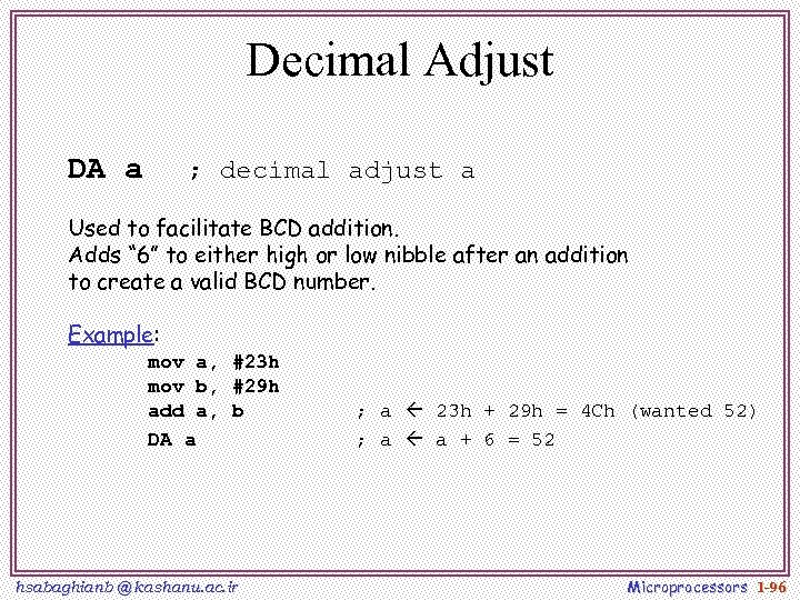
Decimal Adjust DA a ; decimal adjust a Used to facilitate BCD addition. Adds “ 6” to either high or low nibble after an addition to create a valid BCD number. Example: mov a, #23 h mov b, #29 h add a, b DA a hsabaghianb @ kashanu. ac. ir ; a 23 h + 29 h = 4 Ch (wanted 52) ; a a + 6 = 52 Microprocessors 1 -96
Logic Instructions q Bitwise logic operations v (AND, OR, XOR, NOT) q Clear q Rotate q Swap Logic instructions do NOT affect the flags in PSW hsabaghianb @ kashanu. ac. ir Microprocessors 1 -97
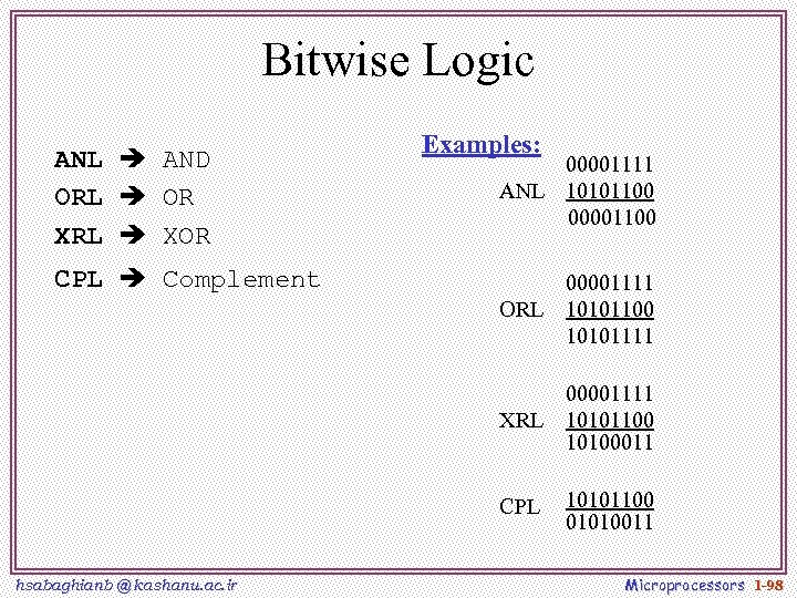
Bitwise Logic ANL AND ORL OR XRL XOR Examples: 00001111 ANL 10101100 00001100 CPL Complement ORL XRL 00001111 10101100 10100011 CPL hsabaghianb @ kashanu. ac. ir 00001111 10101100 10101111 10101100 01010011 Microprocessors 1 -98
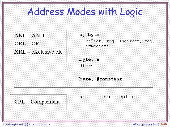
Address Modes with Logic ANL – AND ORL – OR XRL – e. Xclusive o. R a, byte direct, reg. indirect, reg, immediate byte, a direct byte, #constant CPL – Complement hsabaghianb @ kashanu. ac. ir a ex: cpl a Microprocessors 1 -99
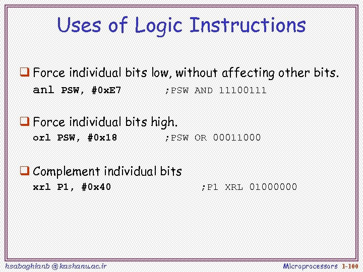
Uses of Logic Instructions q Force individual bits low, without affecting other bits. anl PSW, #0 x. E 7 ; PSW AND 11100111 q Force individual bits high. orl PSW, #0 x 18 ; PSW OR 00011000 q Complement individual bits xrl P 1, #0 x 40 hsabaghianb @ kashanu. ac. ir ; P 1 XRL 01000000 Microprocessors 1 -100
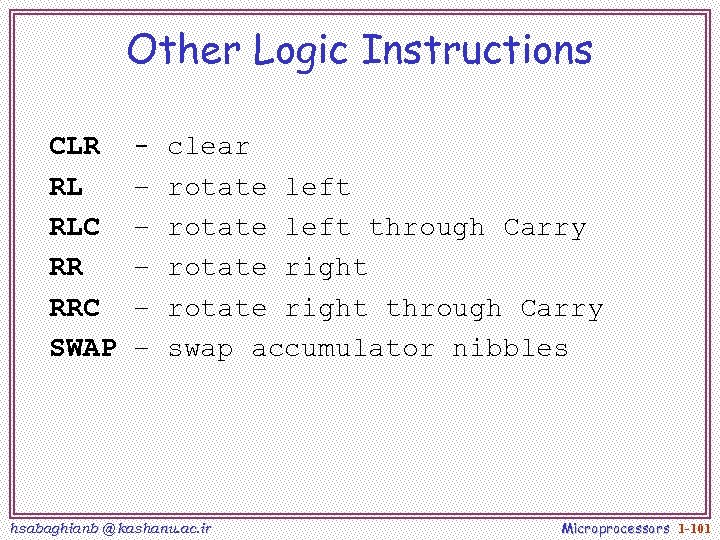
Other Logic Instructions CLR RL RLC RR RRC SWAP – – – clear rotate left through Carry rotate right through Carry swap accumulator nibbles hsabaghianb @ kashanu. ac. ir Microprocessors 1 -101
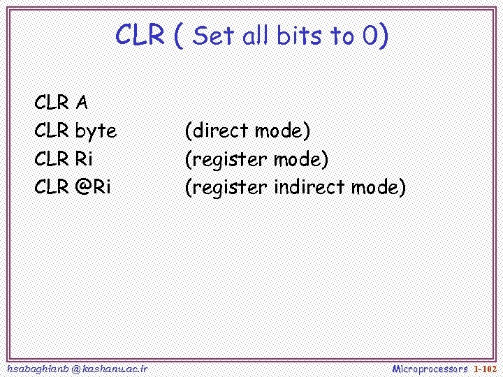
CLR ( Set all bits to 0) CLR A CLR byte CLR Ri CLR @Ri hsabaghianb @ kashanu. ac. ir (direct mode) (register indirect mode) Microprocessors 1 -102
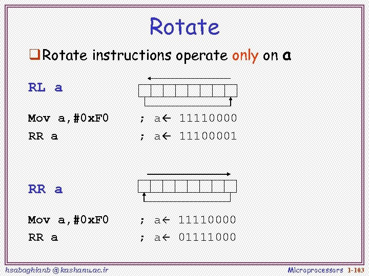
Rotate q Rotate instructions operate only on a RL a Mov a, #0 x. F 0 RR a ; a 11110000 ; a 11100001 RR a Mov a, #0 x. F 0 RR a hsabaghianb @ kashanu. ac. ir ; a 11110000 ; a 01111000 Microprocessors 1 -103
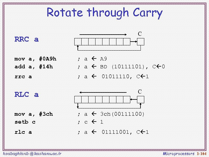
Rotate through Carry RRC a C mov a, #0 A 9 h add a, #14 h ; a A 9 ; a BD (10111101), C 0 rrc a ; a 01011110, C 1 RLC a C mov a, #3 ch setb c ; a 3 ch(00111100) ; c 1 rlc a ; a 01111001, C 1 hsabaghianb @ kashanu. ac. ir Microprocessors 1 -104
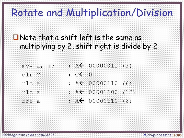
Rotate and Multiplication/Division q Note that a shift left is the same as multiplying by 2, shift right is divide by 2 mov clr rlc rrc a, #3 C a a a hsabaghianb @ kashanu. ac. ir ; ; ; A C A A A 00000011 0 000001100 00000110 (3) (6) (12) (6) Microprocessors 1 -105
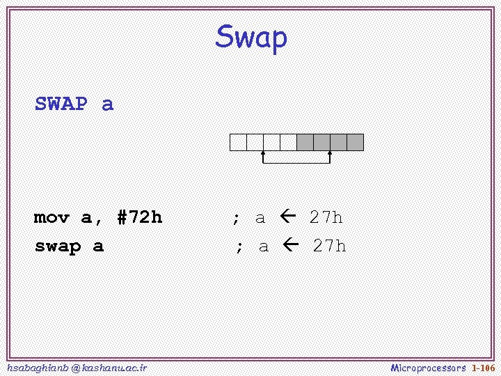
Swap SWAP a mov a, #72 h swap a hsabaghianb @ kashanu. ac. ir ; a 27 h Microprocessors 1 -106
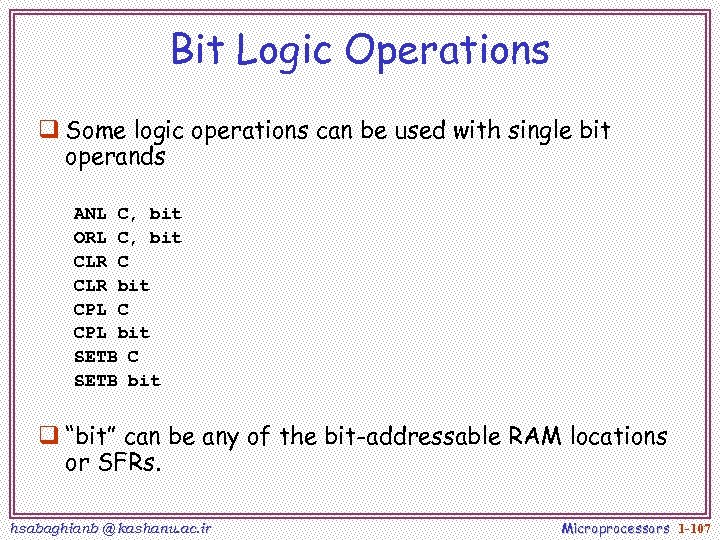
Bit Logic Operations q Some logic operations can be used with single bit operands ANL C, bit ORL C, bit CLR C CLR bit CPL C CPL bit SETB C SETB bit q “bit” can be any of the bit-addressable RAM locations or SFRs. hsabaghianb @ kashanu. ac. ir Microprocessors 1 -107

Shift/Mutliply Example q Program segment to multiply by 2 and add 1. hsabaghianb @ kashanu. ac. ir Microprocessors 1 -108

Program Flow Control q Unconditional jumps (“go to”) q Conditional jumps q Call and return hsabaghianb @ kashanu. ac. ir Microprocessors 1 -109
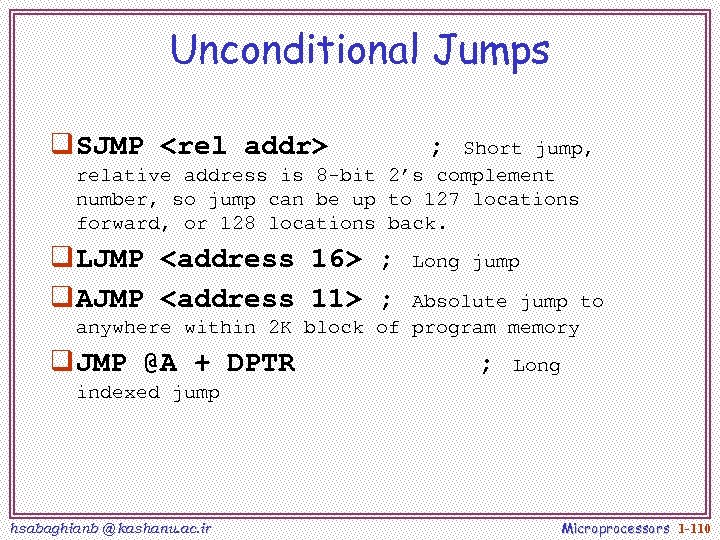
Unconditional Jumps q SJMP <rel addr> ; Short jump, relative address is 8 -bit 2’s complement number, so jump can be up to 127 locations forward, or 128 locations back. q LJMP <address 16> ; q AJMP <address 11> ; Long jump Absolute jump to anywhere within 2 K block of program memory q JMP @A + DPTR ; Long indexed jump hsabaghianb @ kashanu. ac. ir Microprocessors 1 -110
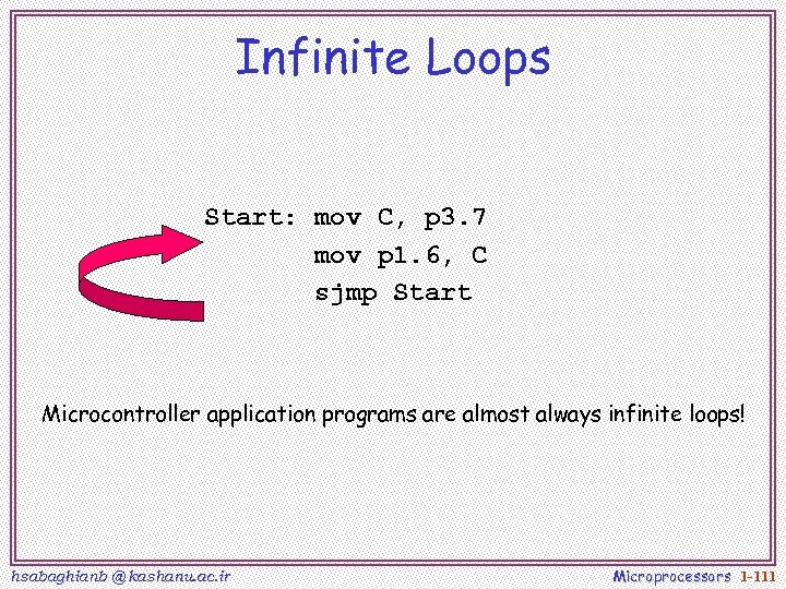
Infinite Loops Start: mov C, p 3. 7 mov p 1. 6, C sjmp Start Microcontroller application programs are almost always infinite loops! hsabaghianb @ kashanu. ac. ir Microprocessors 1 -111
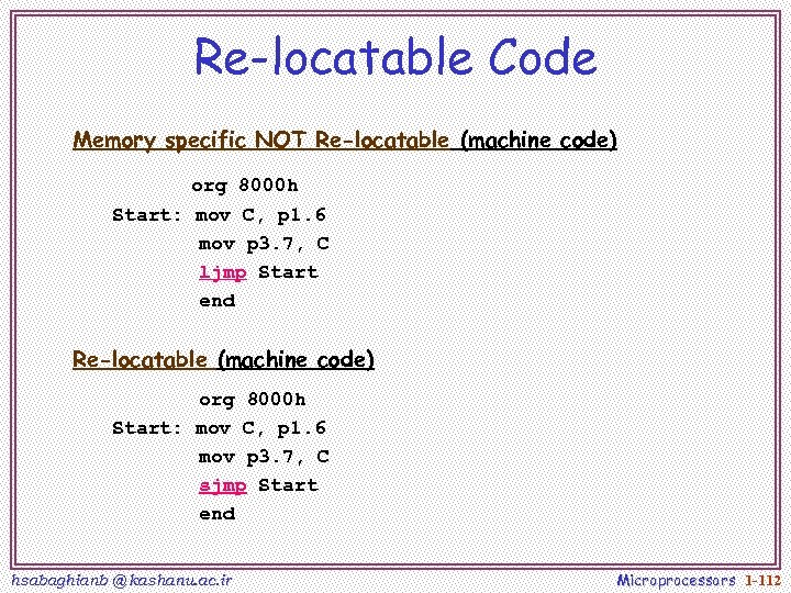
Re-locatable Code Memory specific NOT Re-locatable (machine code) org 8000 h Start: mov C, p 1. 6 mov p 3. 7, C ljmp Start end Re-locatable (machine code) org 8000 h Start: mov C, p 1. 6 mov p 3. 7, C sjmp Start end hsabaghianb @ kashanu. ac. ir Microprocessors 1 -112
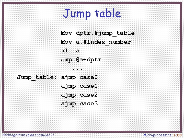
Jump table Mov dptr, #jump_table Mov a, #index_number Rl a Jmp @a+dptr. . . Jump_table: ajmp case 0 ajmp case 1 ajmp case 2 ajmp case 3 hsabaghianb @ kashanu. ac. ir Microprocessors 1 -113
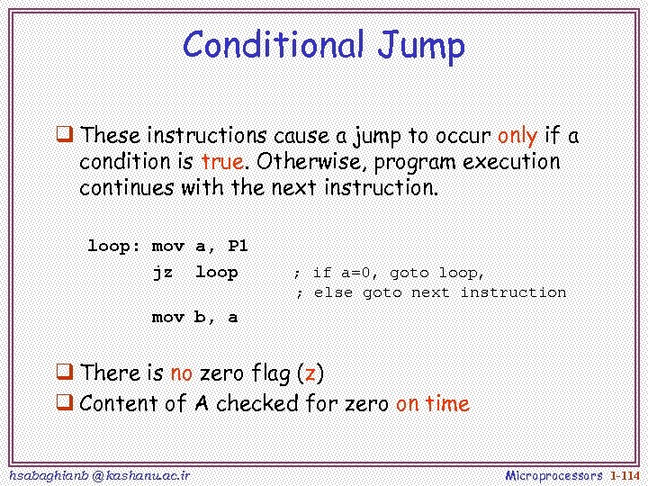
Conditional Jump q These instructions cause a jump to occur only if a condition is true. Otherwise, program execution continues with the next instruction. loop: mov a, P 1 jz loop ; if a=0, goto loop, ; else goto next instruction mov b, a q There is no zero flag (z) q Content of A checked for zero on time hsabaghianb @ kashanu. ac. ir Microprocessors 1 -114
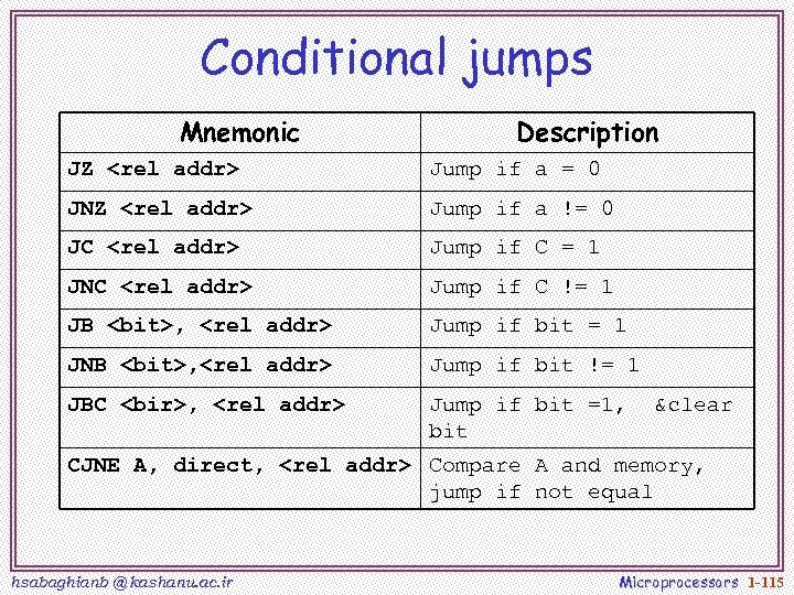
Conditional jumps Mnemonic Description JZ <rel addr> Jump if a = 0 JNZ <rel addr> Jump if a != 0 JC <rel addr> Jump if C = 1 JNC <rel addr> Jump if C != 1 JB <bit>, <rel addr> Jump if bit = 1 JNB <bit>, <rel addr> Jump if bit != 1 JBC <bir>, <rel addr> Jump if bit =1, bit &clear CJNE A, direct, <rel addr> Compare A and memory, jump if not equal hsabaghianb @ kashanu. ac. ir Microprocessors 1 -115
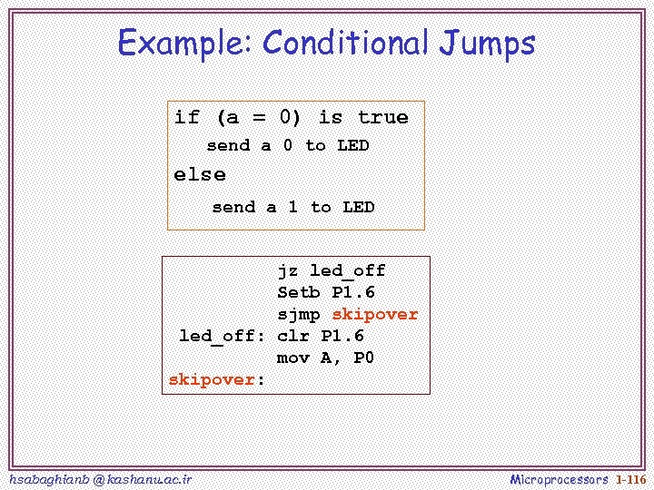
Example: Conditional Jumps if (a = 0) is true send a 0 to LED else send a 1 to LED jz led_off Setb P 1. 6 sjmp skipover led_off: clr P 1. 6 mov A, P 0 skipover: hsabaghianb @ kashanu. ac. ir Microprocessors 1 -116
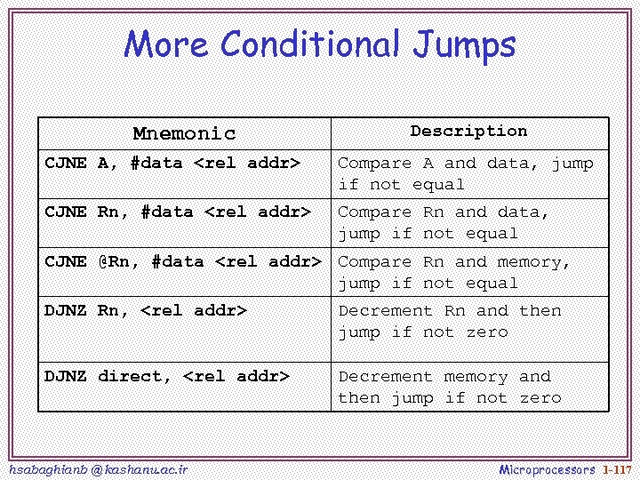
More Conditional Jumps Mnemonic Description CJNE A, #data <rel addr> Compare A and data, jump if not equal CJNE Rn, #data <rel addr> Compare Rn and data, jump if not equal CJNE @Rn, #data <rel addr> Compare Rn and memory, jump if not equal DJNZ Rn, <rel addr> Decrement Rn and then jump if not zero DJNZ direct, <rel addr> Decrement memory and then jump if not zero hsabaghianb @ kashanu. ac. ir Microprocessors 1 -117
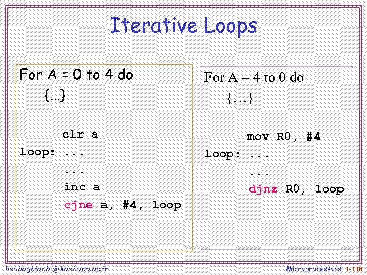
Iterative Loops For A = 0 to 4 do {…} For A = 4 to 0 do {…} clr a loop: . . . inc a cjne a, #4, loop mov R 0, #4 loop: . . . djnz R 0, loop hsabaghianb @ kashanu. ac. ir Microprocessors 1 -118
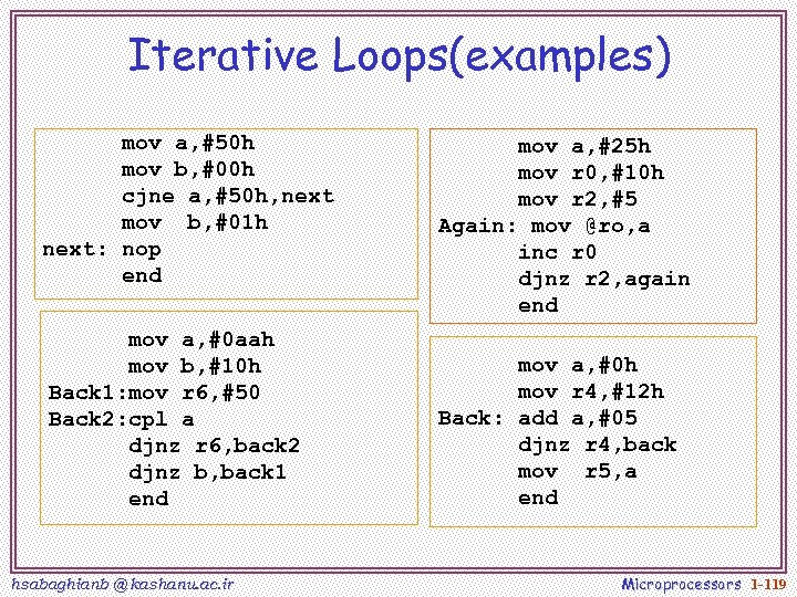
Iterative Loops(examples) mov a, #50 h mov b, #00 h cjne a, #50 h, next mov b, #01 h next: nop end mov a, #0 aah mov b, #10 h Back 1: mov r 6, #50 Back 2: cpl a djnz r 6, back 2 djnz b, back 1 end hsabaghianb @ kashanu. ac. ir mov a, #25 h mov r 0, #10 h mov r 2, #5 Again: mov @ro, a inc r 0 djnz r 2, again end mov a, #0 h mov r 4, #12 h Back: add a, #05 djnz r 4, back mov r 5, a end Microprocessors 1 -119
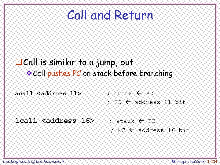
Call and Return q Call is similar to a jump, but v. Call pushes PC on stack before branching acall <address ll> lcall <address 16> ; stack PC ; PC address 11 bit ; stack PC ; PC address 16 bit hsabaghianb @ kashanu. ac. ir Microprocessors 1 -120
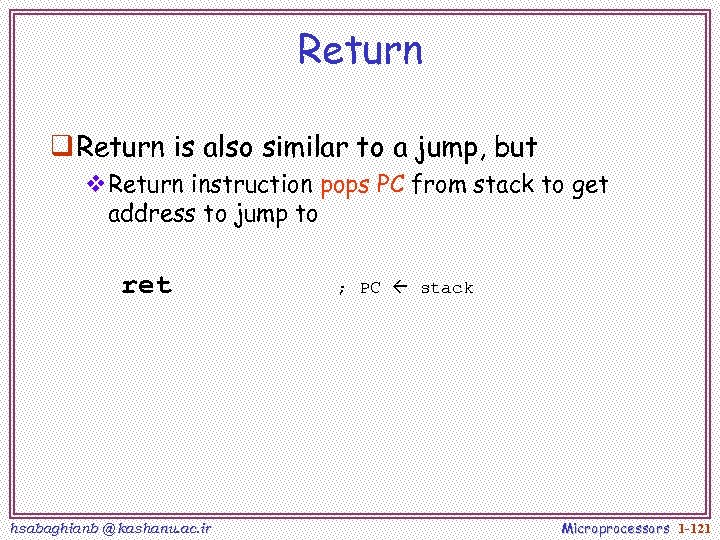
Return q Return is also similar to a jump, but v. Return instruction pops PC from stack to get address to jump to ret hsabaghianb @ kashanu. ac. ir ; PC stack Microprocessors 1 -121
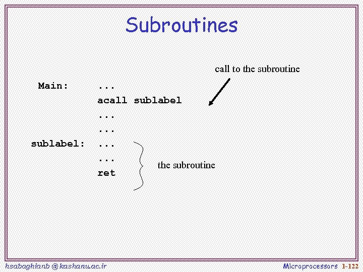
Subroutines call to the subroutine Main: sublabel: . . . acall sublabel. . . the subroutine ret hsabaghianb @ kashanu. ac. ir Microprocessors 1 -122
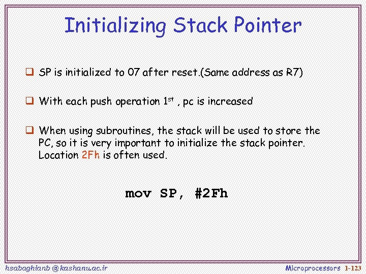
Initializing Stack Pointer q SP is initialized to 07 after reset. (Same address as R 7) q With each push operation 1 st , pc is increased q When using subroutines, the stack will be used to store the PC, so it is very important to initialize the stack pointer. Location 2 Fh is often used. mov SP, #2 Fh hsabaghianb @ kashanu. ac. ir Microprocessors 1 -123
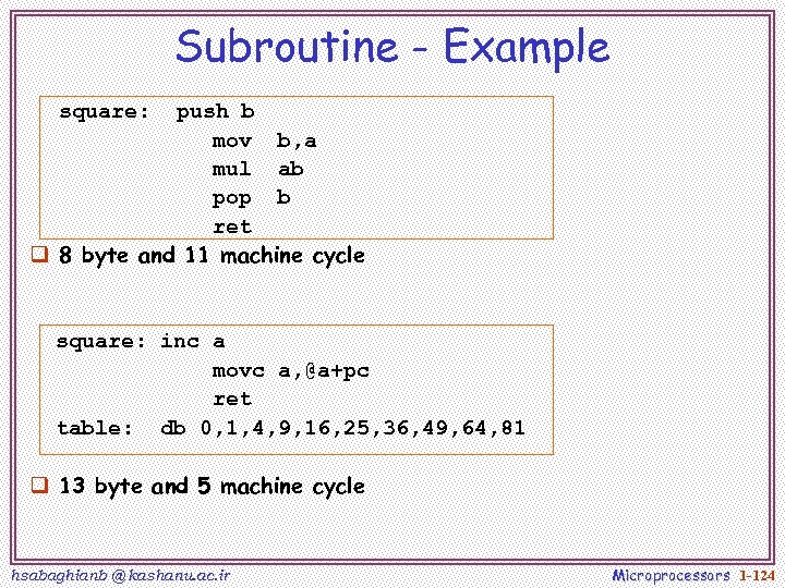
Subroutine - Example square: push b mov b, a mul ab pop b ret q 8 byte and 11 machine cycle square: inc a movc a, @a+pc ret table: db 0, 1, 4, 9, 16, 25, 36, 49, 64, 81 q 13 byte and 5 machine cycle hsabaghianb @ kashanu. ac. ir Microprocessors 1 -124
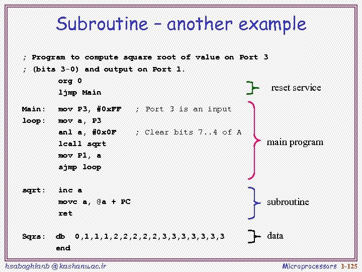
Subroutine – another example ; Program to compute square root of value on Port 3 ; (bits 3 -0) and output on Port 1. org 0 ljmp Main: loop: sqrt: Sqrs: mov P 3, #0 x. FF mov a, P 3 anl a, #0 x 0 F lcall sqrt mov P 1, a sjmp loop ; Port 3 is an input ; Clear bits 7. . 4 of A inc a movc a, @a + PC ret db 0, 1, 1, 1, 2, 2, 2, 3, 3, 3, 3 end hsabaghianb @ kashanu. ac. ir reset service main program subroutine data Microprocessors 1 -125

Why Subroutines? q Subroutines allow us to have "structured" assembly language programs. q This is useful for breaking a large design into manageable parts. q It saves code space when subroutines can be called many times in the same program. hsabaghianb @ kashanu. ac. ir Microprocessors 1 -126
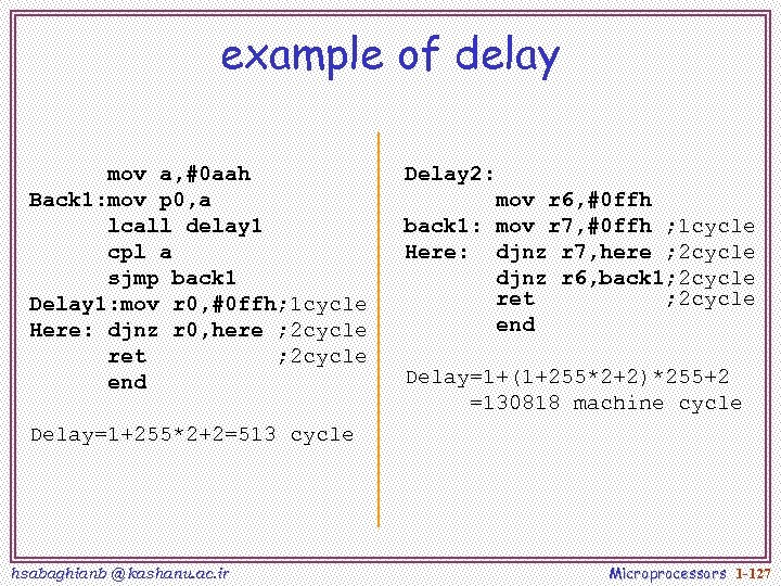
example of delay mov a, #0 aah Back 1: mov p 0, a lcall delay 1 cpl a sjmp back 1 Delay 1: mov r 0, #0 ffh; 1 cycle Here: djnz r 0, here ; 2 cycle ret ; 2 cycle end Delay 2: mov r 6, #0 ffh back 1: mov r 7, #0 ffh ; 1 cycle Here: djnz r 7, here ; 2 cycle djnz r 6, back 1; 2 cycle ret ; 2 cycle end Delay=1+(1+255*2+2)*255+2 =130818 machine cycle Delay=1+255*2+2=513 cycle hsabaghianb @ kashanu. ac. ir Microprocessors 1 -127
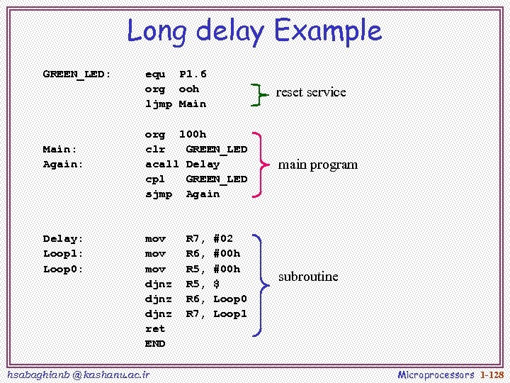
Long delay Example GREEN_LED: Main: Again: Delay: Loop 1: Loop 0: equ P 1. 6 org ooh ljmp Main reset service org 100 h clr GREEN_LED acall Delay cpl GREEN_LED sjmp Again main program mov mov djnz ret END hsabaghianb @ kashanu. ac. ir R 7, R 6, R 5, R 6, R 7, #02 #00 h $ Loop 0 Loop 1 subroutine Microprocessors 1 -128
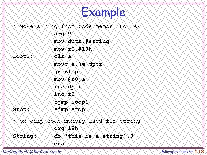
Example ; Move string from code memory to RAM org 0 mov dptr, #string mov r 0, #10 h Loop 1: clr a movc a, @a+dptr jz stop mov @r 0, a inc dptr inc r 0 sjmp loop 1 Stop: sjmp stop ; on-chip code memory used for string org 18 h String: db ‘this is a string’, 0 end hsabaghianb @ kashanu. ac. ir Microprocessors 1 -129
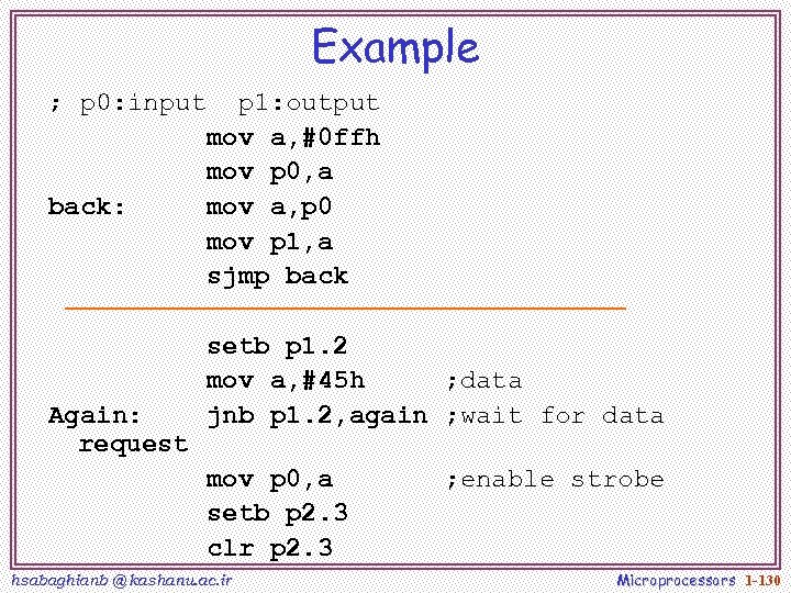
Example ; p 0: input p 1: output mov a, #0 ffh mov p 0, a back: mov a, p 0 mov p 1, a sjmp back Again: request setb p 1. 2 mov a, #45 h ; data jnb p 1. 2, again ; wait for data mov p 0, a setb p 2. 3 clr p 2. 3 hsabaghianb @ kashanu. ac. ir ; enable strobe Microprocessors 1 -130
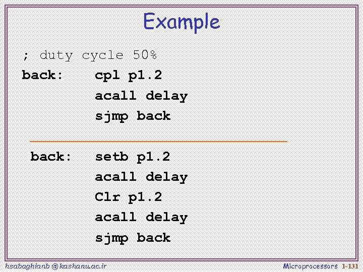
Example ; duty cycle 50% back: cpl p 1. 2 acall delay sjmp back: setb p 1. 2 acall delay Clr p 1. 2 acall delay sjmp back hsabaghianb @ kashanu. ac. ir Microprocessors 1 -131
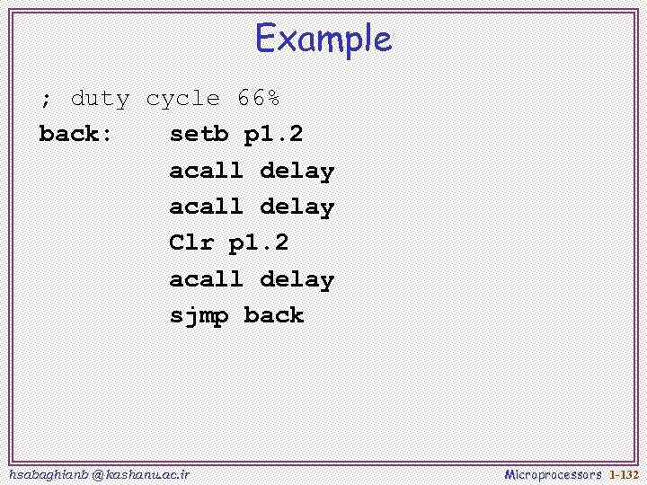
Example ; duty cycle 66% back: setb p 1. 2 acall delay Clr p 1. 2 acall delay sjmp back hsabaghianb @ kashanu. ac. ir Microprocessors 1 -132

8051 timer hsabaghianb @ kashanu. ac. ir Microprocessors 1 -133
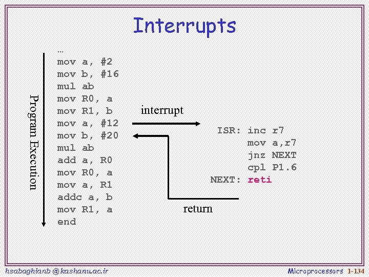
Interrupts Program Execution … mov a, #2 mov b, #16 mul ab mov R 0, a mov R 1, b mov a, #12 mov b, #20 mul ab add a, R 0 mov R 0, a mov a, R 1 addc a, b mov R 1, a end hsabaghianb @ kashanu. ac. ir interrupt ISR: inc r 7 mov a, r 7 jnz NEXT cpl P 1. 6 NEXT: reti return Microprocessors 1 -134
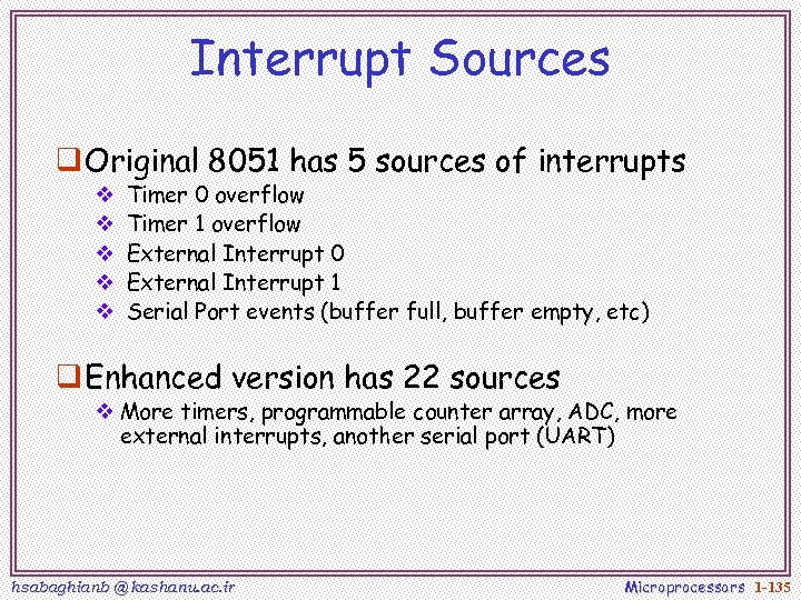
Interrupt Sources q Original 8051 has 5 sources of interrupts v v v Timer 0 overflow Timer 1 overflow External Interrupt 0 External Interrupt 1 Serial Port events (buffer full, buffer empty, etc) q Enhanced version has 22 sources v More timers, programmable counter array, ADC, more external interrupts, another serial port (UART) hsabaghianb @ kashanu. ac. ir Microprocessors 1 -135
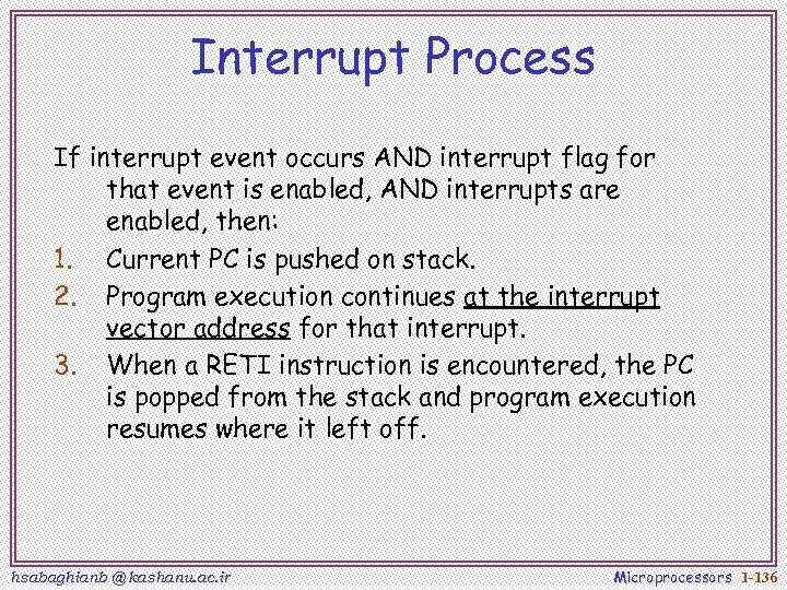
Interrupt Process If interrupt event occurs AND interrupt flag for that event is enabled, AND interrupts are enabled, then: 1. Current PC is pushed on stack. 2. Program execution continues at the interrupt vector address for that interrupt. 3. When a RETI instruction is encountered, the PC is popped from the stack and program execution resumes where it left off. hsabaghianb @ kashanu. ac. ir Microprocessors 1 -136
Interrupt Priorities q What if two interrupt sources interrupt at the same time? q The interrupt with the highest PRIORITY gets serviced first. q All interrupts have a default priority order. q Priority can also be set to “high” or “low”. hsabaghianb @ kashanu. ac. ir Microprocessors 1 -137
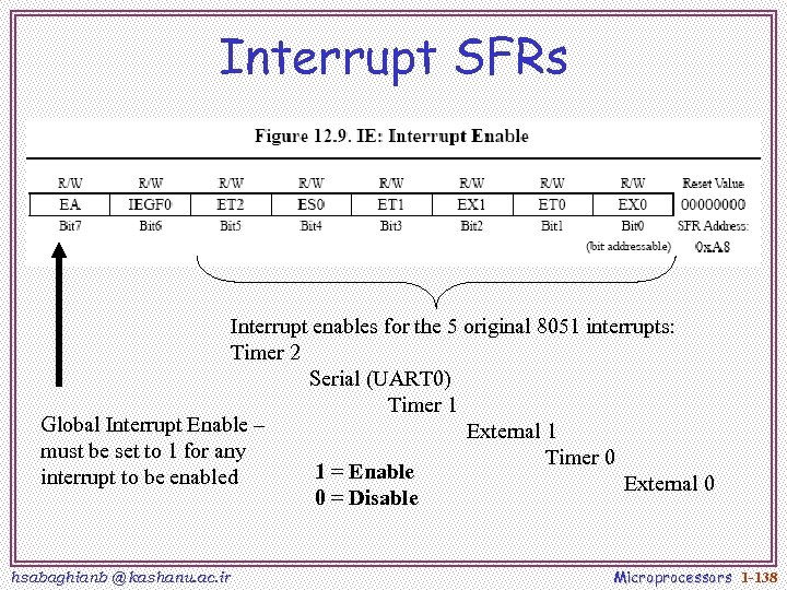
Interrupt SFRs Interrupt enables for the 5 original 8051 interrupts: Timer 2 Serial (UART 0) Timer 1 Global Interrupt Enable – External 1 must be set to 1 for any Timer 0 1 = Enable interrupt to be enabled External 0 0 = Disable hsabaghianb @ kashanu. ac. ir Microprocessors 1 -138
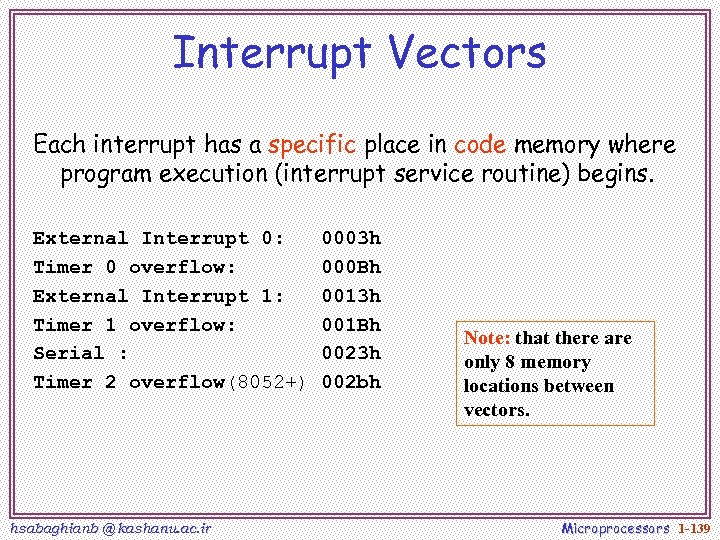
Interrupt Vectors Each interrupt has a specific place in code memory where program execution (interrupt service routine) begins. External Interrupt 0: Timer 0 overflow: External Interrupt 1: Timer 1 overflow: Serial : Timer 2 overflow(8052+) hsabaghianb @ kashanu. ac. ir 0003 h 000 Bh 0013 h 001 Bh 0023 h 002 bh Note: that there are only 8 memory locations between vectors. Microprocessors 1 -139
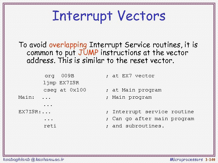
Interrupt Vectors To avoid overlapping Interrupt Service routines, it is common to put JUMP instructions at the vector address. This is similar to the reset vector. org 009 B ljmp EX 7 ISR cseg at 0 x 100 Main: . . . EX 7 ISR: . . . reti hsabaghianb @ kashanu. ac. ir ; at EX 7 vector ; at Main program ; Interrupt service routine ; Can go after main program ; and subroutines. Microprocessors 1 -140
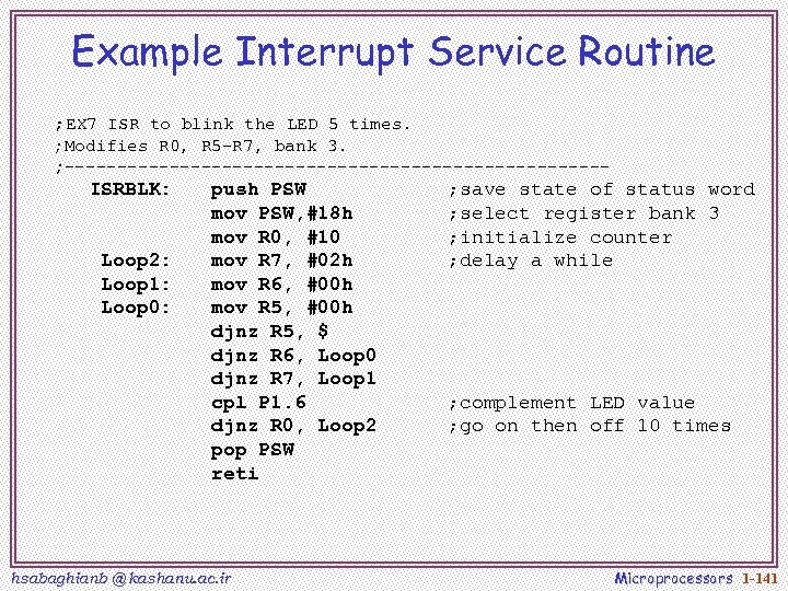
Example Interrupt Service Routine ; EX 7 ISR to blink the LED 5 times. ; Modifies R 0, R 5 -R 7, bank 3. ; -------------------------- ISRBLK: Loop 2: Loop 1: Loop 0: push PSW mov PSW, #18 h mov R 0, #10 mov R 7, #02 h mov R 6, #00 h mov R 5, #00 h djnz R 5, $ djnz R 6, Loop 0 djnz R 7, Loop 1 cpl P 1. 6 djnz R 0, Loop 2 pop PSW reti hsabaghianb @ kashanu. ac. ir ; save state of status word ; select register bank 3 ; initialize counter ; delay a while ; complement LED value ; go on then off 10 times Microprocessors 1 -141
f4c8d14a795df957350863231252f375.ppt