b88ff42555ca36557e91a6bdc64ef4a4.ppt
- Количество слайдов: 87
 The 68 HC 11 Microcontroller Chapter 7: Parallel I/O Ports The 68 HC 11 Microcontroller Han-Way Huang Minnesota State University, Mankato H. Huang Transparency No. 7 -1
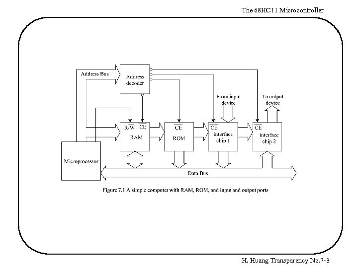
 The 68 HC 11 Microcontroller Basic I/O Concepts Peripheral devices Pieces of equipment that exchange data with a computer. Examples include switches, light-emitting diodes, cathode-ray tube screens, printers, modems, keyboards, and disk drives. Interface (peripheral) chip - A chip whose function is to synchronize data transfer between the CPU and I/O devices. - An interface may consist of control registers, status registers, data direction latches, and control circuitry. - An interface chip has pins that are connected to the CPU and I/O port pins that are connected to the I/O devices. - Each interface chip has a chip enable signal input or inputs, when asserted, allow the interface chip to react to the data transfer request. - Data transfer between an I/O device and the CPU can be proceeded bit-by-bit or in multiple bits. H. Huang Transparency No. 7 -2
 The 68 HC 11 Microcontroller H. Huang Transparency No. 7 -3
 The 68 HC 11 Microcontroller I/O Schemes 1. Isolated I/O scheme - The microprocessor has dedicated instructions for I/O operations - The microprocessor has a separate address space for I/O devices 2. Memory-mapped I/O scheme - The microprocessor uses the same instruction set for I/O operations - The I/O devices and memory components are resident in the same memory space H. Huang Transparency No. 7 -4
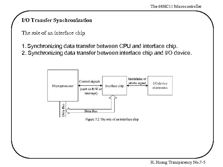 The 68 HC 11 Microcontroller I/O Transfer Synchronization The role of an interface chip 1. Synchronizing data transfer between CPU and interface chip. 2. Synchronizing data transfer between interface chip and I/O device. H. Huang Transparency No. 7 -5
 The 68 HC 11 Microcontroller Synchronizing the Microprocessor and the Interface Chip The polling method 1. for input -- the microprocessor checks a status bit of the interface chip to find out if the interface chip has received new data from the input device. 2. for output -- the microprocessor checks a status bit of the interface chip to find out if it can send new data to the interface chip. The interrupt-driven method 1. for input -- the interface chip interrupts the microprocessor whenever it has received new data from the input device. 2. for output -- the interface chip interrupts the microprocessor whenever it can accept new data from the microprocessor. H. Huang Transparency No. 7 -6
 The 68 HC 11 Microcontroller Synchronizing the Interface Chip and the I/O Devices Brute-force method -- useful when the data timing is unimportant 1. for input -- nothing special is done. The microprocessor reads the interface chip and the interface chip returns the voltage levels on the input port pins to the microprocessor. 2. for output -- nothing special is done. The interface chip places the data that it received from the microprocessor directly on the output port pins. The strobe method -- a strobe signal is used to indicate that data are stable on I/O port pins 1. for input -- the interface chip latches the data into its data register using the strobe signal. 2. for output -- the interface chip places the data on port pins that it received from the microprocessor and asserts the strobe signal. The output device latches the data using the strobe signal. The handshake method -- used when timing is crucial - two handshake signals are used to synchronize the data transfer. One signal, call it H 1, is asserted by the interface chip. The other signal, call it H 2, is asserted by the I/O device. - two handshake modes are available -- pulse mode and interlocked mode. H. Huang Transparency No. 7 -7
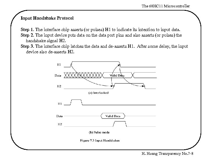 The 68 HC 11 Microcontroller Input Handshake Protocol Step 1. The interface chip asserts (or pulses) H 1 to indicate its intention to input data. Step 2. The input device puts data on the data port pins and also asserts (or pulses) the handshake signal H 2. Step 3. The interface chip latches the data and de-asserts H 1. After some delay, the input device also de-asserts H 2. H. Huang Transparency No. 7 -8
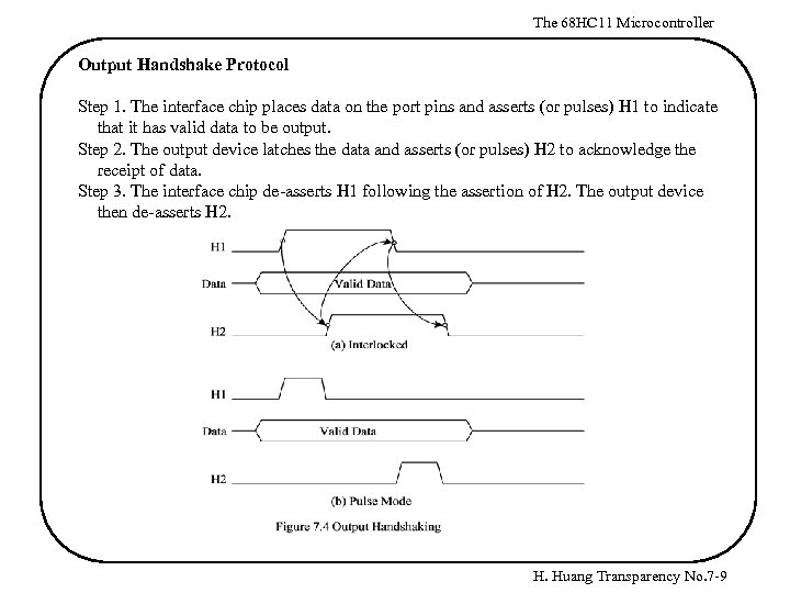 The 68 HC 11 Microcontroller Output Handshake Protocol Step 1. The interface chip places data on the port pins and asserts (or pulses) H 1 to indicate that it has valid data to be output. Step 2. The output device latches the data and asserts (or pulses) H 2 to acknowledge the receipt of data. Step 3. The interface chip de-asserts H 1 following the assertion of H 2. The output device then de-asserts H 2. H. Huang Transparency No. 7 -9
 The 68 HC 11 Microcontroller 68 HC 11 Parallel I/O Overview - The 68 HC 11 A 8 has 40 I/O pins that are arranged in five I/O ports. All I/O pins serve multiple functions. Ports A, B, and E with the exception of port A pin 7 are fixed-direction inputs or outputs. Ports C and D are bi-directional I/O pins under the control of their associated data direction registers. - Port C, port B, the STRA pin, and the STRB pin are used for strobed and handshake parallel I/O, as well as for general-purpose I/O. Port Registers - To input, the 68 HC 11 reads from the port data register - To output, the 68 HC 11 writes into the port data register - All except port C have one data register: PORTA (at $1000) PORTB (at $1004) PORTC (at $1003) PORTCL (at $1005) PORTD (at $1008) PORTE (at $100 A) H. Huang Transparency No. 7 -10
 The 68 HC 11 Microcontroller Fixed Direction I/O (ports A, B, and E) To input from an input port, execute a load instruction with the port data register as the source operand. For example, the following instruction sequence reads a byte from port E: REGBAS PORTE ldx ldaa equ $1000 equ $0 A #REGBAS PORTE, X ; I/O register block base address ; offset of port E data register from REGBAS To output a byte to an output port, write to the port data register directly. For example, the following instruction sequence outputs the value #$38 to port B: REGBAS equ PORTB equ ldx ldaa staa $1000 $04 ; I/O register block base address ; offset of port B data register from REGBAS #$38 PORTB, X H. Huang Transparency No. 7 -11
 The 68 HC 11 Microcontroller Bi-directional I/O (Ports C and D) - Each pin of ports C and D has an associated bit in a specific data register and another in a data direction register. - The primary direction of a pin is set by its associated bit in the data direction register. - When an output pin is read, the value at the input to the pin driver is returned. - The data direction registers are cleared by reset to configure all bi-directional I/O pins for input. - Before performing I/O operation to these two ports, the software should set up the data direction registers of these two ports. H. Huang Transparency No. 7 -12
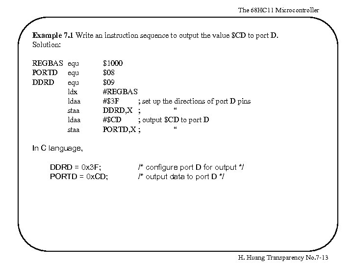 The 68 HC 11 Microcontroller Example 7. 1 Write an instruction sequence to output the value $CD to port D. Solution: REGBAS equ PORTD equ DDRD equ ldx ldaa staa $1000 $08 $09 #REGBAS #$3 F ; set up the directions of port D pins DDRD, X ; “ #$CD ; output $CD to port D PORTD, X ; “ In C language, DDRD = 0 x 3 F; PORTD = 0 x. CD; /* configure port D for output */ /* output data to port D */ H. Huang Transparency No. 7 -13
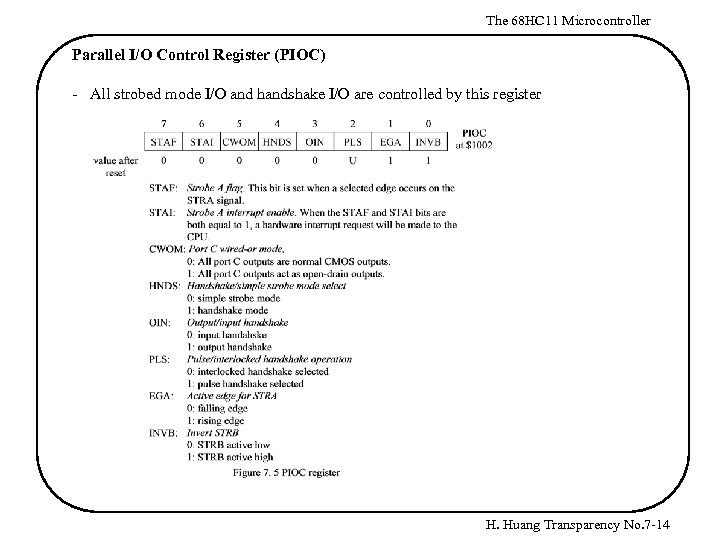 The 68 HC 11 Microcontroller Parallel I/O Control Register (PIOC) - All strobed mode I/O and handshake I/O are controlled by this register H. Huang Transparency No. 7 -14
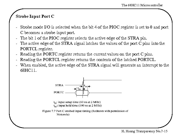 The 68 HC 11 Microcontroller Strobe Input Port C - Strobe mode I/O is selected when the bit 4 of the PIOC register is set to 0 and port C becomes a strobe input port. - The bit 1 of the PIOC register selects the active edge of the STRA pin. - The active edge of the STRA signal latches the values of the port C pins into the PORTCL register. - Reading the PORTC register returns the current values on the port C pins. - Reading the PORTCL register returns the contents of the latched PORTCL. - When enabled, the active edge of the STRA signal will generate an interrupt to the 68 HC 11. H. Huang Transparency No. 7 -15
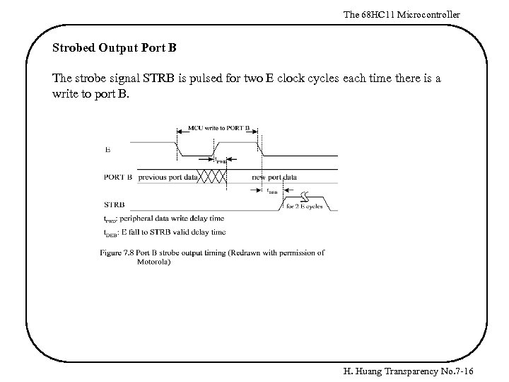 The 68 HC 11 Microcontroller Strobed Output Port B The strobe signal STRB is pulsed for two E clock cycles each time there is a write to port B. H. Huang Transparency No. 7 -16
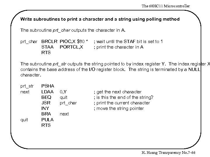
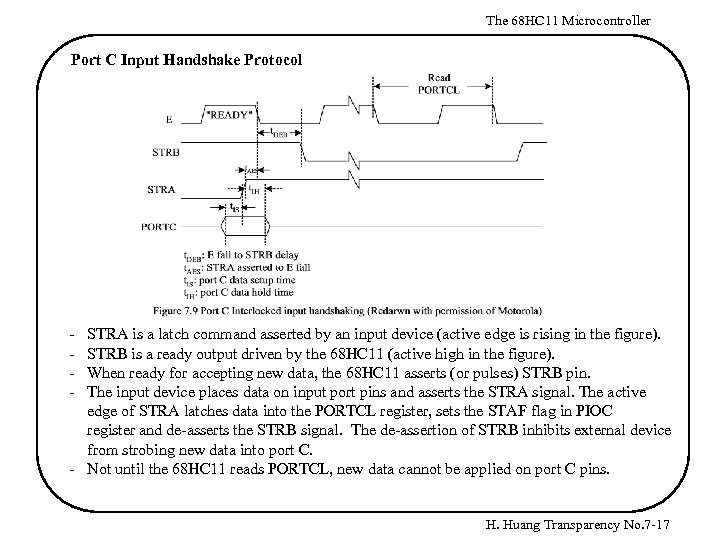 The 68 HC 11 Microcontroller Port C Input Handshake Protocol - STRA is a latch command asserted by an input device (active edge is rising in the figure). STRB is a ready output driven by the 68 HC 11 (active high in the figure). When ready for accepting new data, the 68 HC 11 asserts (or pulses) STRB pin. The input device places data on input port pins and asserts the STRA signal. The active edge of STRA latches data into the PORTCL register, sets the STAF flag in PIOC register and de-asserts the STRB signal. The de-assertion of STRB inhibits external device from strobing new data into port C. - Not until the 68 HC 11 reads PORTCL, new data cannot be applied on port C pins. H. Huang Transparency No. 7 -17
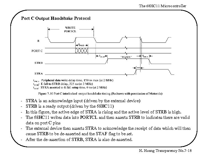 The 68 HC 11 Microcontroller Port C Output Handshake Protocol - STRA is an acknowledge input (driven by the external device) STRB is a ready output (driven by the 68 HC 11) In this figure, the active edge of STRA is rising and the active level of STRB is high. The 68 HC 11 writes data into PORTCL and then asserts STRB to indicates there are valid data on port C pins - The external device then asserts STRA to acknowledge the receipt of data which will then cause STRB to be de-asserted and the STAF flag to be set. - After the de-assertion of STRB, STRA is also de-asserted. H. Huang Transparency No. 7 -18
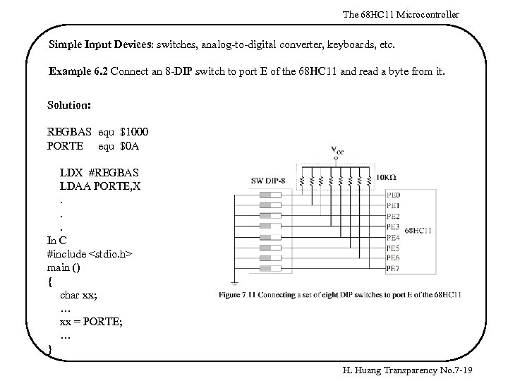 The 68 HC 11 Microcontroller Simple Input Devices: switches, analog-to-digital converter, keyboards, etc. Example 6. 2 Connect an 8 -DIP switch to port E of the 68 HC 11 and read a byte from it. Solution: REGBAS equ $1000 PORTE equ $0 A LDX #REGBAS LDAA PORTE, X. . . In C #include
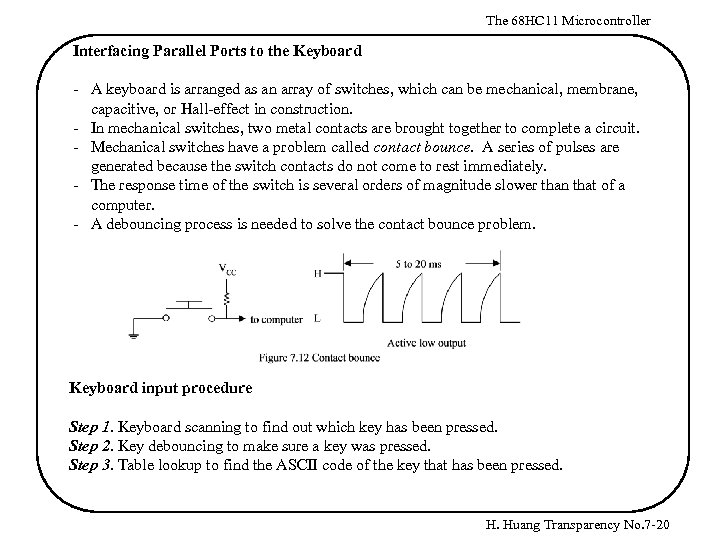 The 68 HC 11 Microcontroller Interfacing Parallel Ports to the Keyboard - A keyboard is arranged as an array of switches, which can be mechanical, membrane, capacitive, or Hall-effect in construction. - In mechanical switches, two metal contacts are brought together to complete a circuit. - Mechanical switches have a problem called contact bounce. A series of pulses are generated because the switch contacts do not come to rest immediately. - The response time of the switch is several orders of magnitude slower than that of a computer. - A debouncing process is needed to solve the contact bounce problem. Keyboard input procedure Step 1. Keyboard scanning to find out which key has been pressed. Step 2. Key debouncing to make sure a key was pressed. Step 3. Table lookup to find the ASCII code of the key that has been pressed. H. Huang Transparency No. 7 -20
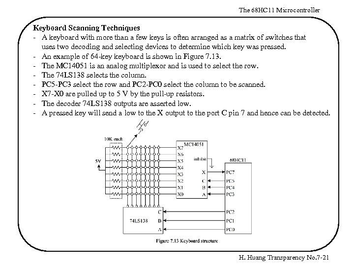 The 68 HC 11 Microcontroller Keyboard Scanning Techniques - A keyboard with more than a few keys is often arranged as a matrix of switches that uses two decoding and selecting devices to determine which key was pressed. - An example of 64 -key keyboard is shown in Figure 7. 13. - The MC 14051 is an analog multiplexor and is used to select the row. - The 74 LS 138 selects the column. - PC 5 -PC 3 select the row and PC 2 -PC 0 select the column to be scanned. - X 7 -X 0 are pulled up to 5 V by the pull-up resistors. - The decoder 74 LS 138 outputs are asserted low. - A pressed key will send a low to the X output to the port C pin 7 and hence can be detected. H. Huang Transparency No. 7 -21
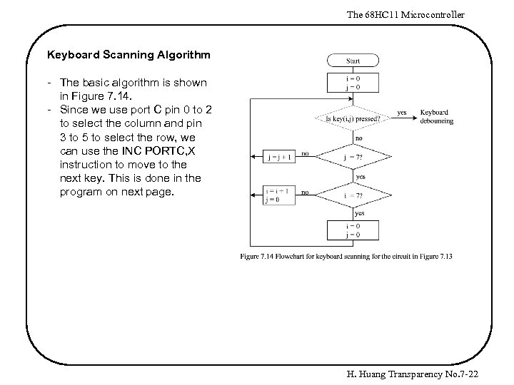 The 68 HC 11 Microcontroller Keyboard Scanning Algorithm - The basic algorithm is shown in Figure 7. 14. - Since we use port C pin 0 to 2 to select the column and pin 3 to 5 to select the row, we can use the INC PORTC, X instruction to move to the next key. This is done in the program on next page. H. Huang Transparency No. 7 -22
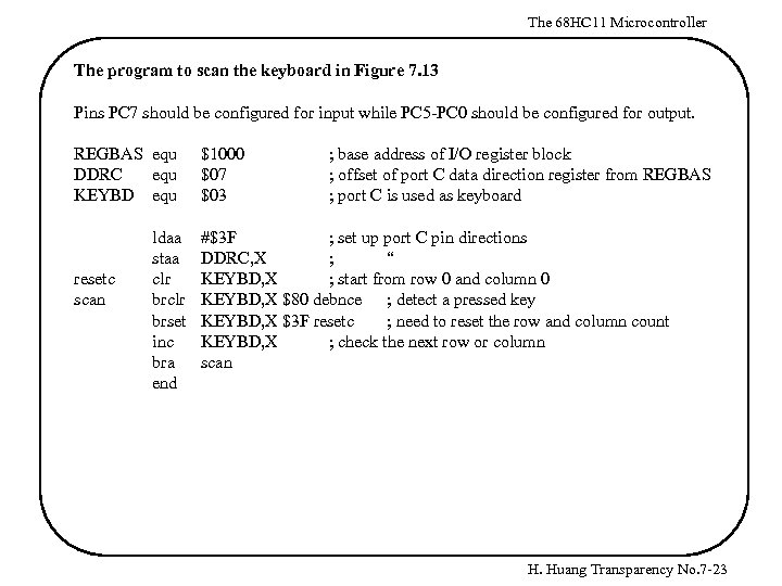 The 68 HC 11 Microcontroller The program to scan the keyboard in Figure 7. 13 Pins PC 7 should be configured for input while PC 5 -PC 0 should be configured for output. REGBAS equ DDRC equ KEYBD equ resetc scan ldaa staa clr brset inc bra end $1000 $07 $03 ; base address of I/O register block ; offset of port C data direction register from REGBAS ; port C is used as keyboard #$3 F ; set up port C pin directions DDRC, X ; “ KEYBD, X ; start from row 0 and column 0 KEYBD, X $80 debnce ; detect a pressed key KEYBD, X $3 F resetc ; need to reset the row and column count KEYBD, X ; check the next row or column scan H. Huang Transparency No. 7 -23
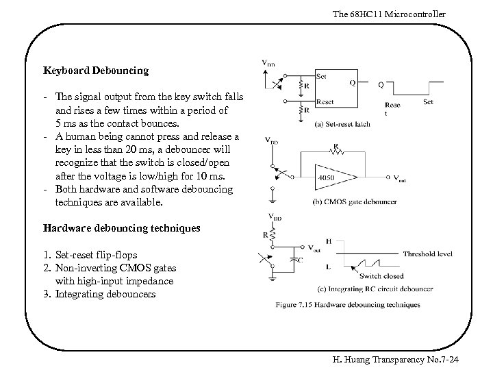 The 68 HC 11 Microcontroller Keyboard Debouncing - The signal output from the key switch falls and rises a few times within a period of 5 ms as the contact bounces. - A human being cannot press and release a key in less than 20 ms, a debouncer will recognize that the switch is closed/open after the voltage is low/high for 10 ms. - Both hardware and software debouncing techniques are available. Hardware debouncing techniques 1. Set-reset flip-flops 2. Non-inverting CMOS gates with high-input impedance 3. Integrating debouncers H. Huang Transparency No. 7 -24
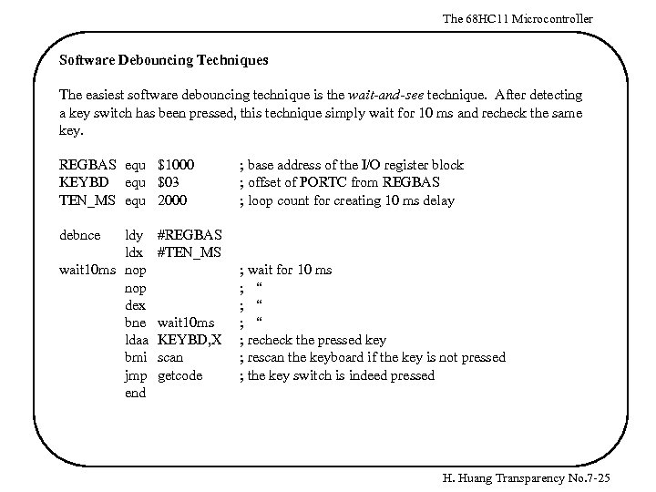 The 68 HC 11 Microcontroller Software Debouncing Techniques The easiest software debouncing technique is the wait-and-see technique. After detecting a key switch has been pressed, this technique simply wait for 10 ms and recheck the same key. REGBAS equ $1000 KEYBD equ $03 TEN_MS equ 2000 debnce ldy ldx wait 10 ms nop dex bne ldaa bmi jmp end ; base address of the I/O register block ; offset of PORTC from REGBAS ; loop count for creating 10 ms delay #REGBAS #TEN_MS wait 10 ms KEYBD, X scan getcode ; wait for 10 ms ; “ ; “ ; recheck the pressed key ; rescan the keyboard if the key is not pressed ; the key switch is indeed pressed H. Huang Transparency No. 7 -25
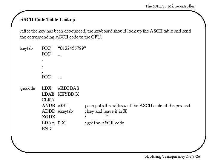 The 68 HC 11 Microcontroller ASCII Code Table Lookup After the key has been debounced, the keyboard should look up the ASCII table and send the corresponding ASCII code to the CPU. keytab getcode FCC. . . FCC “ 0123456789”. . . LDX LDAB CLRA ANDB ADDD XGDX LDAA END #REGBAS KEYBD, X … #$3 f #keytab 0, X ; compute the address of the ASCII code of the pressed ; key and leave it in X ; “ ; get the ASCII code H. Huang Transparency No. 7 -26
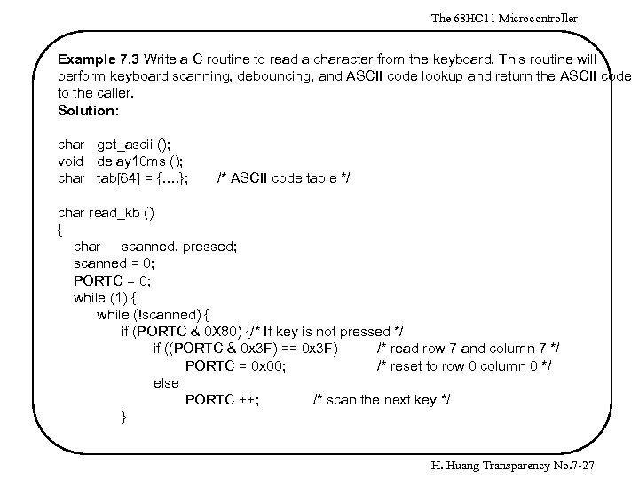 The 68 HC 11 Microcontroller Example 7. 3 Write a C routine to read a character from the keyboard. This routine will perform keyboard scanning, debouncing, and ASCII code lookup and return the ASCII code to the caller. Solution: char get_ascii (); void delay 10 ms (); char tab[64] = {…. }; /* ASCII code table */ char read_kb () { char scanned, pressed; scanned = 0; PORTC = 0; while (1) { while (!scanned) { if (PORTC & 0 X 80) {/* If key is not pressed */ if ((PORTC & 0 x 3 F) == 0 x 3 F) /* read row 7 and column 7 */ PORTC = 0 x 00; /* reset to row 0 column 0 */ else PORTC ++; /* scan the next key */ } H. Huang Transparency No. 7 -27
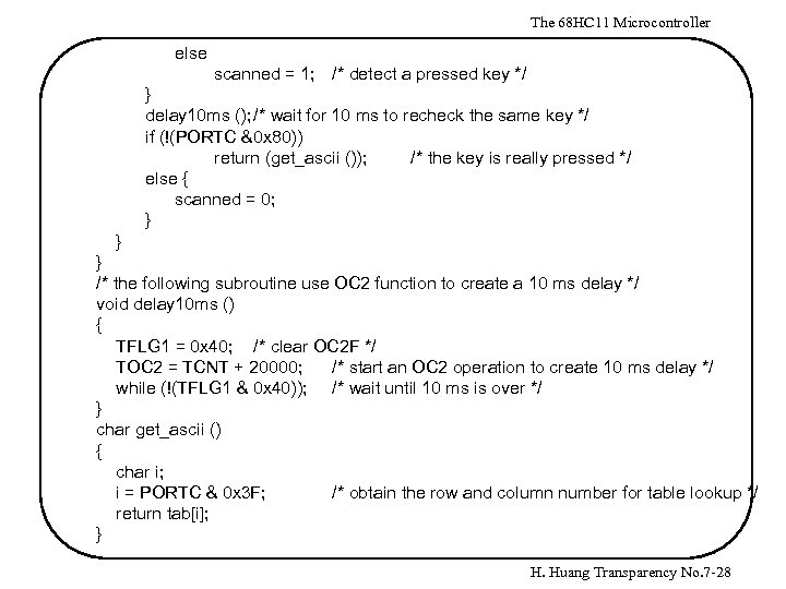 The 68 HC 11 Microcontroller else scanned = 1; /* detect a pressed key */ } delay 10 ms (); /* wait for 10 ms to recheck the same key */ if (!(PORTC &0 x 80)) return (get_ascii ()); /* the key is really pressed */ else { scanned = 0; } } } /* the following subroutine use OC 2 function to create a 10 ms delay */ void delay 10 ms () { TFLG 1 = 0 x 40; /* clear OC 2 F */ TOC 2 = TCNT + 20000; /* start an OC 2 operation to create 10 ms delay */ while (!(TFLG 1 & 0 x 40)); /* wait until 10 ms is over */ } char get_ascii () { char i; i = PORTC & 0 x 3 F; /* obtain the row and column number for table lookup */ return tab[i]; } H. Huang Transparency No. 7 -28
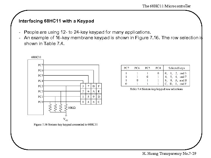 The 68 HC 11 Microcontroller Interfacing 68 HC 11 with a Keypad - People are using 12 - to 24 -key keypad for many applications. - An example of 16 -key membrane keypad is shown in Figure 7. 16. The row selection is shown in Table 7. 4. H. Huang Transparency No. 7 -29
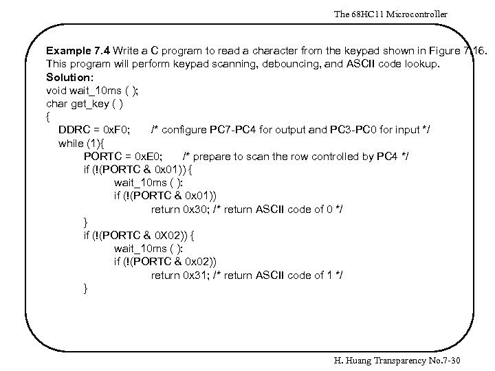 The 68 HC 11 Microcontroller Example 7. 4 Write a C program to read a character from the keypad shown in Figure 7. 16. This program will perform keypad scanning, debouncing, and ASCII code lookup. Solution: void wait_10 ms ( ); char get_key ( ) { DDRC = 0 x. F 0; /* configure PC 7 -PC 4 for output and PC 3 -PC 0 for input */ while (1){ PORTC = 0 x. E 0; /* prepare to scan the row controlled by PC 4 */ if (!(PORTC & 0 x 01)) { wait_10 ms ( ): if (!(PORTC & 0 x 01)) return 0 x 30; /* return ASCII code of 0 */ } if (!(PORTC & 0 X 02)) { wait_10 ms ( ): if (!(PORTC & 0 x 02)) return 0 x 31; /* return ASCII code of 1 */ } H. Huang Transparency No. 7 -30
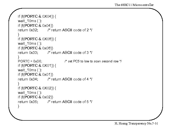 The 68 HC 11 Microcontroller if (!(PORTC & 0 X 04)) { wait_10 ms ( ): if (!(PORTC & 0 x 04)) return 0 x 32; /* return ASCII code of 2 */ } if (!(PORTC & 0 X 08)) { wait_10 ms ( ): if (!(PORTC & 0 x 08)) return 0 x 33; /* return ASCII code of 3 */ } PORTC = 0 x. D 0; /* set PC 5 to low to scan second row */ if (!(PORTC & 0 X 01)) { wait_10 ms ( ): if (!(PORTC & 0 x 01)) return 0 x 34; /* return ASCII code of 4 */ } if (!(PORTC & 0 X 02)) { wait_10 ms ( ): if (!(PORTC & 0 x 02)) return 0 x 35; /* return ASCII code of 5 */ } H. Huang Transparency No. 7 -31
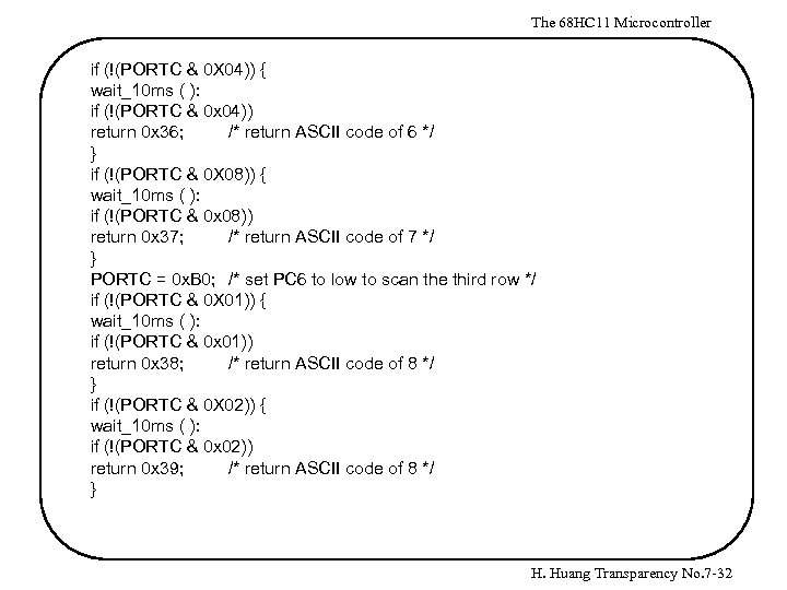 The 68 HC 11 Microcontroller if (!(PORTC & 0 X 04)) { wait_10 ms ( ): if (!(PORTC & 0 x 04)) return 0 x 36; /* return ASCII code of 6 */ } if (!(PORTC & 0 X 08)) { wait_10 ms ( ): if (!(PORTC & 0 x 08)) return 0 x 37; /* return ASCII code of 7 */ } PORTC = 0 x. B 0; /* set PC 6 to low to scan the third row */ if (!(PORTC & 0 X 01)) { wait_10 ms ( ): if (!(PORTC & 0 x 01)) return 0 x 38; /* return ASCII code of 8 */ } if (!(PORTC & 0 X 02)) { wait_10 ms ( ): if (!(PORTC & 0 x 02)) return 0 x 39; /* return ASCII code of 8 */ } H. Huang Transparency No. 7 -32
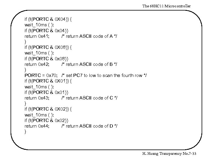 The 68 HC 11 Microcontroller if (!(PORTC & 0 X 04)) { wait_10 ms ( ): if (!(PORTC & 0 x 04)) return 0 x 41; /* return ASCII code of A */ } if (!(PORTC & 0 X 08)) { wait_10 ms ( ): if (!(PORTC & 0 x 08)) return 0 x 42; /* return ASCII code of B */ } PORTC = 0 x 70; /* set PC 7 to low to scan the fourth row */ if (!(PORTC & 0 X 01)) { wait_10 ms ( ): if (!(PORTC & 0 x 01)) return 0 x 43; /* return ASCII code of C */ } if (!(PORTC & 0 X 02)) { wait_10 ms ( ): if (!(PORTC & 0 x 02)) return 0 x 44; /* return ASCII code of D */ } H. Huang Transparency No. 7 -33
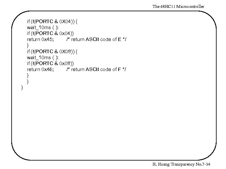 The 68 HC 11 Microcontroller if (!(PORTC & 0 X 04)) { wait_10 ms ( ): if (!(PORTC & 0 x 04)) return 0 x 45; /* return ASCII code of E */ } if (!(PORTC & 0 X 08)) { wait_10 ms ( ): if (!(PORTC & 0 x 08)) return 0 x 46; /* return ASCII code of F */ } } } H. Huang Transparency No. 7 -34
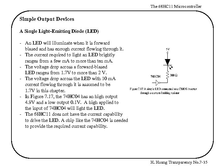 The 68 HC 11 Microcontroller Simple Output Devices A Single Light-Emitting Diode (LED) - An LED will illuminate when it is forward biased and has enough current flowing through it. - The current required to light an LED brightly ranges from a few m. A to more than ten m. A. - The voltage drop across a forward-biased LED ranges from 1. 7 V to more than 2 V. - The voltage drop across the LED with 10 m. A current flowing through it is assumed to be 1. 7 V in this chapter. - In Figure 7. 17, the 74 HC 04 has an high output 4. 9 V and a low output 0. 1 V. A high applied to the input of 74 HC 04 will light the LED. - The 68 HC 11 does not have the current capability to drive the LED. A chip like the 74 HC 04 is needed to provide the required current capability. H. Huang Transparency No. 7 -35
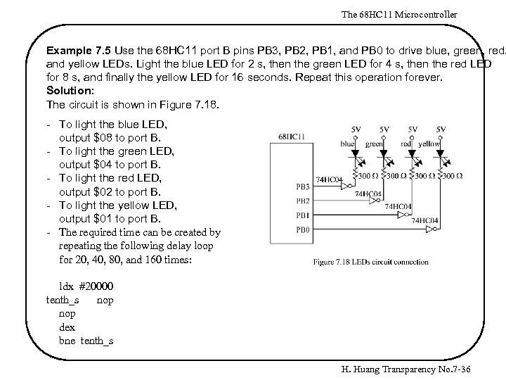 The 68 HC 11 Microcontroller Example 7. 5 Use the 68 HC 11 port B pins PB 3, PB 2, PB 1, and PB 0 to drive blue, green, red, and yellow LEDs. Light the blue LED for 2 s, then the green LED for 4 s, then the red LED for 8 s, and finally the yellow LED for 16 seconds. Repeat this operation forever. Solution: The circuit is shown in Figure 7. 18. - To light the blue LED, output $08 to port B. - To light the green LED, output $04 to port B. - To light the red LED, output $02 to port B. - To light the yellow LED, output $01 to port B. - The required time can be created by repeating the following delay loop for 20, 40, 80, and 160 times: ldx #20000 tenth_s nop dex bne tenth_s H. Huang Transparency No. 7 -36
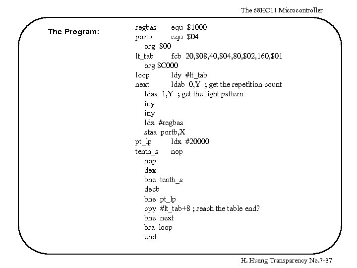 The 68 HC 11 Microcontroller The Program: regbas equ $1000 portb equ $04 org $00 lt_tab fcb 20, $08, 40, $04, 80, $02, 160, $01 org $C 000 loop ldy #lt_tab next ldab 0, Y ; get the repetition count ldaa 1, Y ; get the light pattern iny ldx #regbas staa portb, X pt_lp ldx #20000 tenth_s nop dex bne tenth_s decb bne pt_lp cpy #lt_tab+8 ; reach the table end? bne next bra loop end H. Huang Transparency No. 7 -37
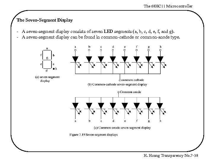 The 68 HC 11 Microcontroller The Seven-Segment Display - A seven-segment display consists of seven LED segments (a, b, c, d, e, f, and g). - A seven-segment display can be found in common-cathode or common-anode type. H. Huang Transparency No. 7 -38
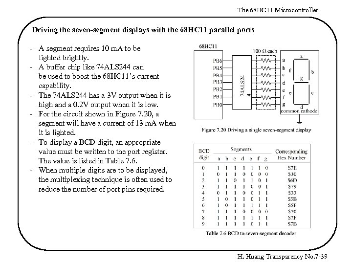 The 68 HC 11 Microcontroller Driving the seven-segment displays with the 68 HC 11 parallel ports - A segment requires 10 m. A to be lighted brightly. - A buffer chip like 74 ALS 244 can be used to boost the 68 HC 11’s current capability. - The 74 ALS 244 has a 3 V output when it is high and a 0. 2 V output when it is low. - For the circuit shown in Figure 7. 20, a segment will have a current of 13 m. A when it is lighted. - To display a BCD digit, an appropriate value must be written to the port register. The value is listed in Table 7. 6. - When multiple digits are to be displayed, the multiplexing technique is often used to reduce the number of port pins required. H. Huang Transparency No. 7 -39
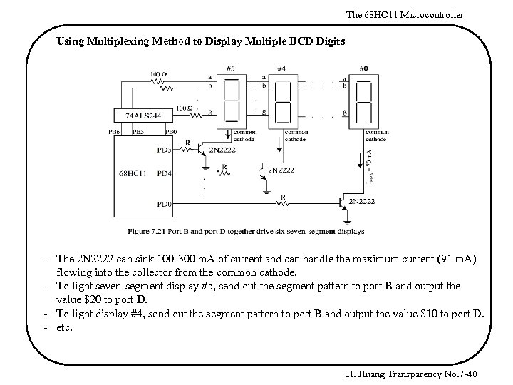 The 68 HC 11 Microcontroller Using Multiplexing Method to Display Multiple BCD Digits - The 2 N 2222 can sink 100 -300 m. A of current and can handle the maximum current (91 m. A) flowing into the collector from the common cathode. - To light seven-segment display #5, send out the segment pattern to port B and output the value $20 to port D. - To light display #4, send out the segment pattern to port B and output the value $10 to port D. - etc. H. Huang Transparency No. 7 -40
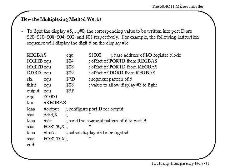 The 68 HC 11 Microcontroller How the Multiplexing Method Works - To light the display #5, …, #0, the corresponding value to be written into port D are $20, $10, $08, $04, $02, and $01 respectively. For example, the following instruction sequence will display the digit 6 on the display #3: REGBAS equ $1000 ; base address of I/O register block PORTB equ $04 ; offset of PORTB from REGBAS PORTDequ $08 ; offset of PORTD from REGBAS DDRD equ $09 ; offset of DDRD from REGBAS six equ $7 D ; segment pattern of 6 third equ $08 ; value to allow display #3 to light output equ $3 F org $C 000 ldx #REGBAS ldaa #output ; configure port D for output staa ddrd, X ; “ ldaa #six ; send the segment pattern of 6 to port B staa PORTB, X ; “ ldaa #third ; select display #3 to be lighted staa PORTD, X ; “ end H. Huang Transparency No. 7 -41
 The 68 HC 11 Microcontroller In C language, DDRD = 0 x 3 F; PORTB = 0 x 5 F; PORTD = 0 x 08; Principle of Multiplexing multiple displays: Persistence of vision. As long as one and only one display is lighted and then turned off for a short period of time within one second all digits will appear to be lighted simultaneously. H. Huang Transparency No. 7 -42
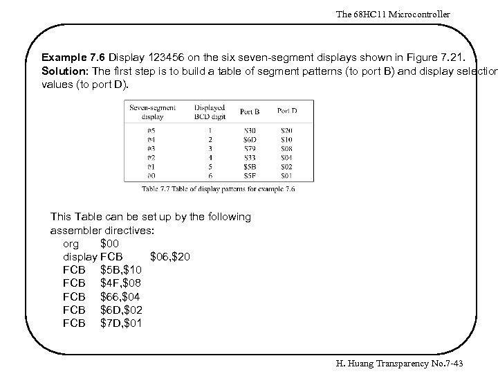 The 68 HC 11 Microcontroller Example 7. 6 Display 123456 on the six seven-segment displays shown in Figure 7. 21. Solution: The first step is to build a table of segment patterns (to port B) and display selection values (to port D). This Table can be set up by the following assembler directives: org $00 display FCB $06, $20 FCB $5 B, $10 FCB $4 F, $08 FCB $66, $04 FCB $6 D, $02 FCB $7 D, $01 H. Huang Transparency No. 7 -43
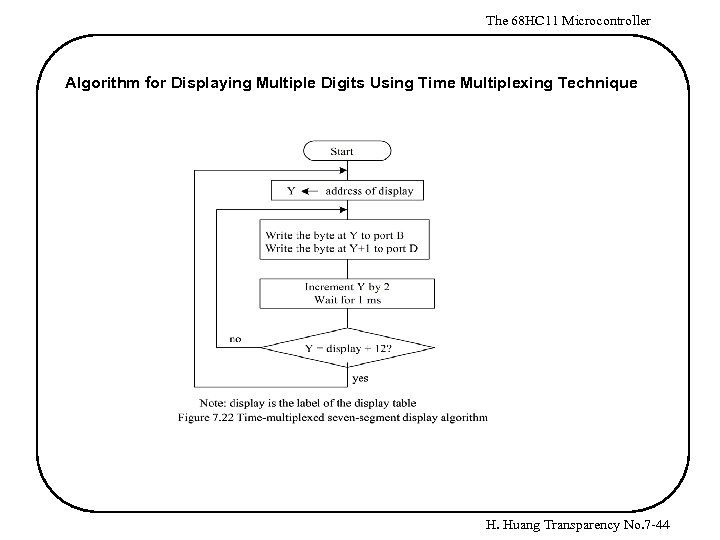 The 68 HC 11 Microcontroller Algorithm for Displaying Multiple Digits Using Time Multiplexing Technique H. Huang Transparency No. 7 -44
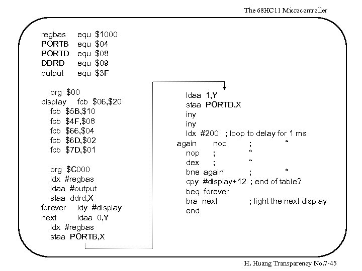 The 68 HC 11 Microcontroller regbas PORTB PORTD DDRD output equ equ equ $1000 $04 $08 $09 $3 F org $00 display fcb $06, $20 fcb $5 B, $10 fcb $4 F, $08 fcb $66, $04 fcb $6 D, $02 fcb $7 D, $01 org $C 000 ldx #regbas ldaa #output staa ddrd, X forever ldy #display next ldaa 0, Y ldx #regbas staa PORTB, X ldaa 1, Y staa PORTD, X iny ldx #200 ; loop to delay for 1 ms again nop ; “ dex ; “ bne again ; “ cpy #display+12 ; end of table? beq forever bra next ; light the next display end H. Huang Transparency No. 7 -45
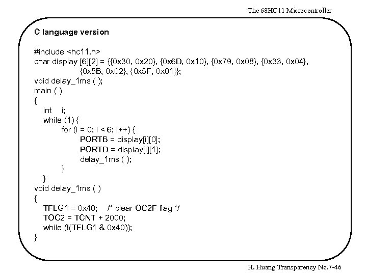 The 68 HC 11 Microcontroller C language version #include
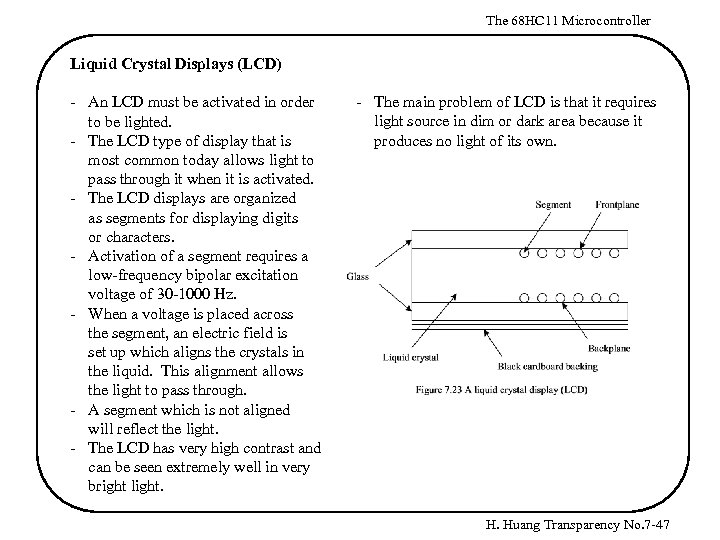 The 68 HC 11 Microcontroller Liquid Crystal Displays (LCD) - An LCD must be activated in order to be lighted. - The LCD type of display that is most common today allows light to pass through it when it is activated. - The LCD displays are organized as segments for displaying digits or characters. - Activation of a segment requires a low-frequency bipolar excitation voltage of 30 -1000 Hz. - When a voltage is placed across the segment, an electric field is set up which aligns the crystals in the liquid. This alignment allows the light to pass through. - A segment which is not aligned will reflect the light. - The LCD has very high contrast and can be seen extremely well in very bright light. - The main problem of LCD is that it requires light source in dim or dark area because it produces no light of its own. H. Huang Transparency No. 7 -47
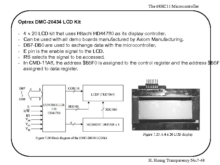 The 68 HC 11 Microcontroller Optrex DMC-20434 LCD Kit - 4 20 LCD kit that uses Hitachi HD 44780 as its display controller. Can be used with all demo boards manufactured by Axiom Manufacturing. DB 7 -DB 0 are used to exchange data with the microcontroller. E pin is the enable signal to the LCD. RS selects the signal to be accessed. In CMD-11 A 8, the address $B 5 F 0 is assigned to the control register and the address $B 5 F 1 assigned to data register. H. Huang Transparency No. 7 -48
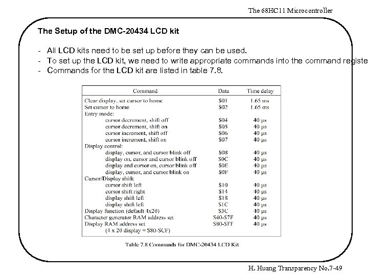 The 68 HC 11 Microcontroller The Setup of the DMC-20434 LCD kit - All LCD kits need to be set up before they can be used. - To set up the LCD kit, we need to write appropriate commands into the command register - Commands for the LCD kit are listed in table 7. 8. H. Huang Transparency No. 7 -49
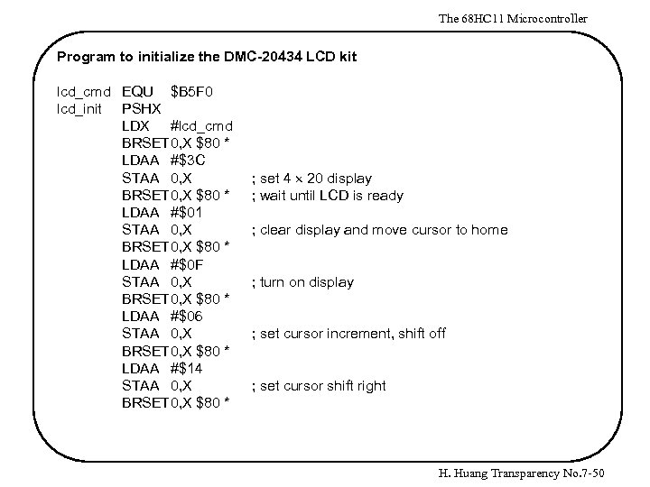 The 68 HC 11 Microcontroller Program to initialize the DMC-20434 LCD kit lcd_cmd EQU $B 5 F 0 lcd_init PSHX LDX #lcd_cmd BRSET 0, X $80 * LDAA #$3 C STAA 0, X BRSET 0, X $80 * LDAA #$01 STAA 0, X BRSET 0, X $80 * LDAA #$0 F STAA 0, X BRSET 0, X $80 * LDAA #$06 STAA 0, X BRSET 0, X $80 * LDAA #$14 STAA 0, X BRSET 0, X $80 * ; set 4 20 display ; wait until LCD is ready ; clear display and move cursor to home ; turn on display ; set cursor increment, shift off ; set cursor shift right H. Huang Transparency No. 7 -50
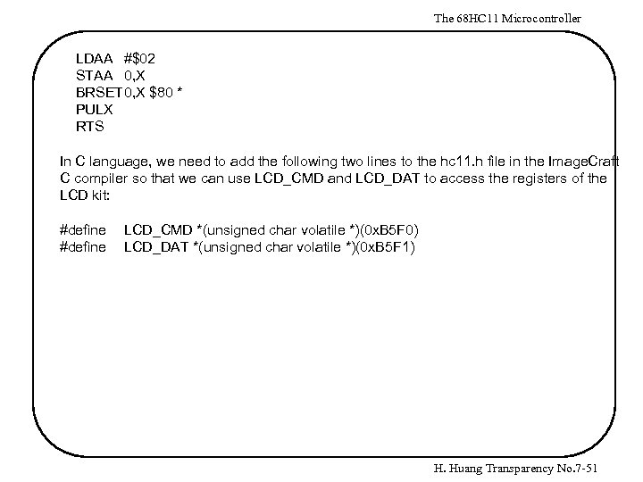 The 68 HC 11 Microcontroller LDAA #$02 STAA 0, X BRSET 0, X $80 * PULX RTS In C language, we need to add the following two lines to the hc 11. h file in the Image. Craft C compiler so that we can use LCD_CMD and LCD_DAT to access the registers of the LCD kit: #define LCD_CMD *(unsigned char volatile *)(0 x. B 5 F 0) LCD_DAT *(unsigned char volatile *)(0 x. B 5 F 1) H. Huang Transparency No. 7 -51
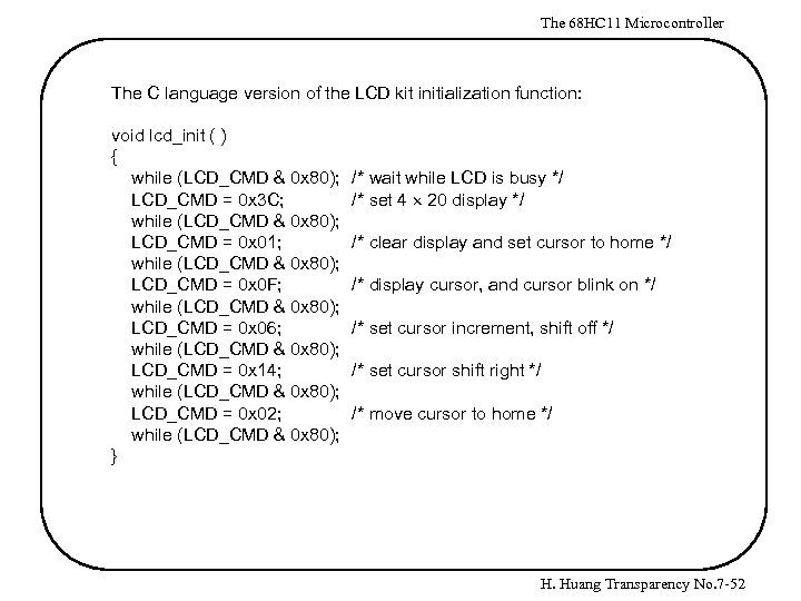 The 68 HC 11 Microcontroller The C language version of the LCD kit initialization function: void lcd_init ( ) { while (LCD_CMD & 0 x 80); LCD_CMD = 0 x 3 C; while (LCD_CMD & 0 x 80); LCD_CMD = 0 x 01; while (LCD_CMD & 0 x 80); LCD_CMD = 0 x 0 F; while (LCD_CMD & 0 x 80); LCD_CMD = 0 x 06; while (LCD_CMD & 0 x 80); LCD_CMD = 0 x 14; while (LCD_CMD & 0 x 80); LCD_CMD = 0 x 02; while (LCD_CMD & 0 x 80); } /* wait while LCD is busy */ /* set 4 20 display */ /* clear display and set cursor to home */ /* display cursor, and cursor blink on */ /* set cursor increment, shift off */ /* set cursor shift right */ /* move cursor to home */ H. Huang Transparency No. 7 -52
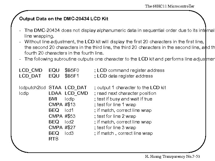 The 68 HC 11 Microcontroller Output Data on the DMC-20434 LCD Kit - The DMC-20434 does not display alphanumeric data in sequential order due to its internal line wrapping. - Without line adjustment, the LCD kit will display the first 20 characters in the first line, the second 20 characters in the third line, the third 20 characters in the second line, and th fourth 20 characters in the fourth line. - The following subroutine outputs one character to the LCD kit and performs line adjustmen LCD_CMD LCD_DAT EQU $B 5 F 0 $B 5 F 1 lcdputch 2 lcd STAA LCD_DAT lcdlp LDAA LCD_CMD BMI lcdlp CMPA #$13 BEQ lcd 1 CMPA #$53 BEQ lcd 2 CMPA #$27 BEQ lcd 3 RTS ; LCD command register address ; LCD data register address ; output 1 character to the LCD kit ; read next character position ; test if busy and wait if true ; test for line 1 wrap ; if match, correct line wrap ; test for line 2 wrap ; if match, correct line wrap ; test for line 3 wrap ; if match , correct line wrap H. Huang Transparency No. 7 -53
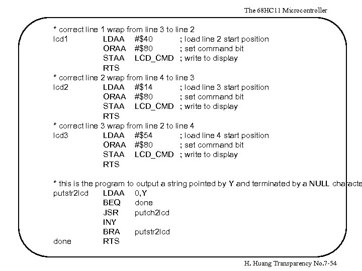 The 68 HC 11 Microcontroller * correct line 1 wrap from line 3 to line 2 lcd 1 LDAA #$40 ; load line 2 start position ORAA #$80 ; set command bit STAA LCD_CMD ; write to display RTS * correct line 2 wrap from line 4 to line 3 lcd 2 LDAA #$14 ; load line 3 start position ORAA #$80 ; set command bit STAA LCD_CMD ; write to display RTS * correct line 3 wrap from line 2 to line 4 lcd 3 LDAA #$54 ; load line 4 start position ORAA #$80 ; set command bit STAA LCD_CMD ; write to display RTS * this is the program to output a string pointed by Y and terminated by a NULL characte putstr 2 lcd LDAA 0, Y BEQ done JSR putch 2 lcd INY BRA putstr 2 lcd done RTS H. Huang Transparency No. 7 -54
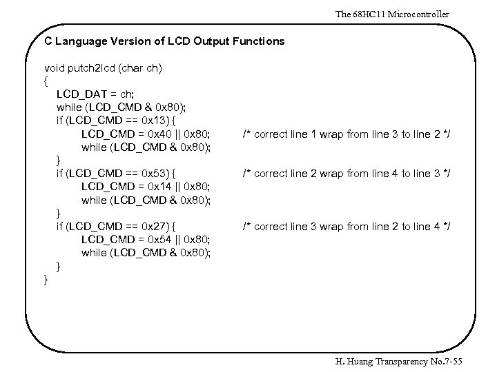 The 68 HC 11 Microcontroller C Language Version of LCD Output Functions void putch 2 lcd (char ch) { LCD_DAT = ch; while (LCD_CMD & 0 x 80); if (LCD_CMD == 0 x 13) { LCD_CMD = 0 x 40 || 0 x 80; while (LCD_CMD & 0 x 80); } if (LCD_CMD == 0 x 53) { LCD_CMD = 0 x 14 || 0 x 80; while (LCD_CMD & 0 x 80); } if (LCD_CMD == 0 x 27) { LCD_CMD = 0 x 54 || 0 x 80; while (LCD_CMD & 0 x 80); } } /* correct line 1 wrap from line 3 to line 2 */ /* correct line 2 wrap from line 4 to line 3 */ /* correct line 3 wrap from line 2 to line 4 */ H. Huang Transparency No. 7 -55
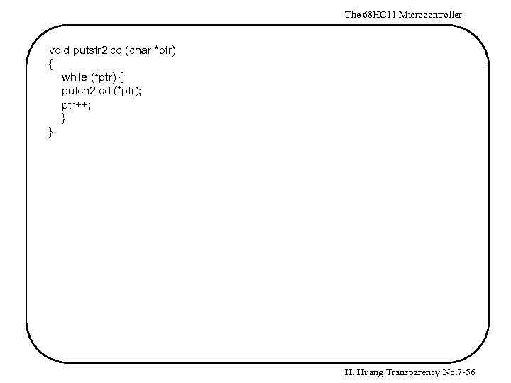 The 68 HC 11 Microcontroller void putstr 2 lcd (char *ptr) { while (*ptr) { putch 2 lcd (*ptr); ptr++; } } H. Huang Transparency No. 7 -56
 The 68 HC 11 Microcontroller Digital to Analog Converter - D/A conversion is required when a digital code must be converted to an analog signal. - A general D/A converter consists of a network of precision resistors, input switches, and level shifters that activate the switches that convert a digital code to an analog voltage or current. - D/A converters have a fixed or variable reference voltage , which can be generated either internally or externally. - The reference voltage determines the switching threshold of the precision switches that for the impedance network that controls the value of the output signal. - Fixed reference D/A converts have current or voltage output values that are proportionally to the digital input. - Multiplying D/A converters produce an output signal that is proportional to the product of a varying reference level and a digital code. H. Huang Transparency No. 7 -57
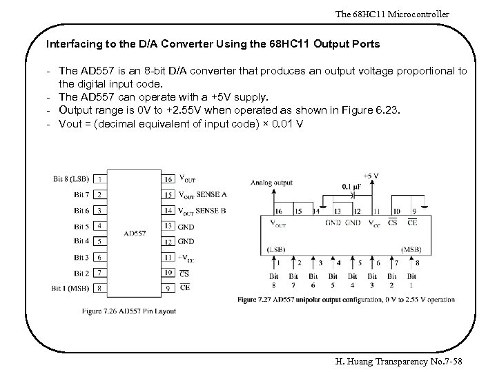 The 68 HC 11 Microcontroller Interfacing to the D/A Converter Using the 68 HC 11 Output Ports - The AD 557 is an 8 -bit D/A converter that produces an output voltage proportional to the digital input code. - The AD 557 can operate with a +5 V supply. - Output range is 0 V to +2. 55 V when operated as shown in Figure 6. 23. - Vout = (decimal equivalent of input code) × 0. 01 V H. Huang Transparency No. 7 -58
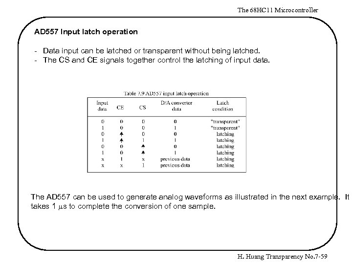 The 68 HC 11 Microcontroller AD 557 Input latch operation - Data input can be latched or transparent without being latched. - The CS and CE signals together control the latching of input data. The AD 557 can be used to generate analog waveforms as illustrated in the next example. It takes 1 ms to complete the conversion of one sample. H. Huang Transparency No. 7 -59
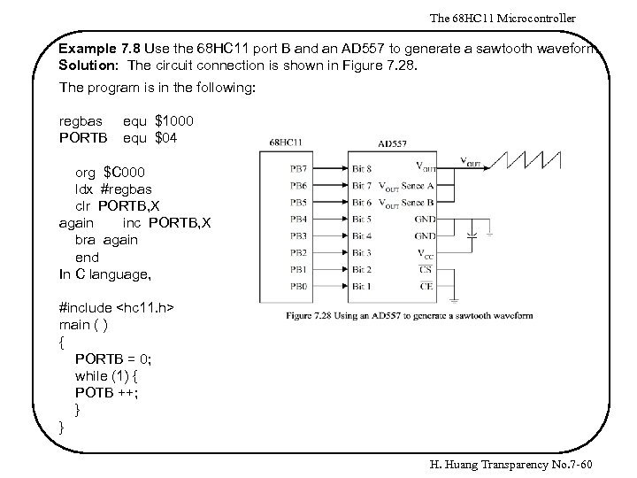 The 68 HC 11 Microcontroller Example 7. 8 Use the 68 HC 11 port B and an AD 557 to generate a sawtooth waveform. Solution: The circuit connection is shown in Figure 7. 28. The program is in the following: regbas PORTB equ $1000 equ $04 org $C 000 ldx #regbas clr PORTB, X again inc PORTB, X bra again end In C language, #include
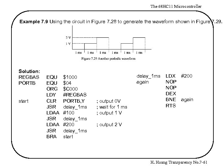 The 68 HC 11 Microcontroller Example 7. 9 Using the circuit in Figure 7. 28 to generate the waveform shown in Figure 7. 29. Solution: REGBAS PORTB start EQU ORG LDY CLR JSR LDAA JSR BRA $1000 $04 $C 000 #REGBAS PORTB, Y delay_1 ms #100 delay_1 ms #200 delay_1 ms start delay_1 ms again ; output 0 V ; wait for 1 ms ; output 1 V LDX #200 NOP DEX BNE again RTS ; output 2 V H. Huang Transparency No. 7 -61
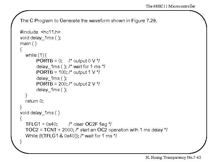 The 68 HC 11 Microcontroller The C Program to Generate the waveform shown in Figure 7. 29. #include
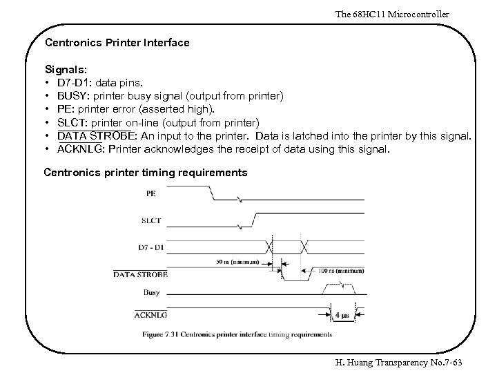 The 68 HC 11 Microcontroller Centronics Printer Interface Signals: • D 7 -D 1: data pins. • BUSY: printer busy signal (output from printer) • PE: printer error (asserted high). • SLCT: printer on-line (output from printer) • DATA STROBE: An input to the printer. Data is latched into the printer by this signal. • ACKNLG: Printer acknowledges the receipt of data using this signal. Centronics printer timing requirements H. Huang Transparency No. 7 -63
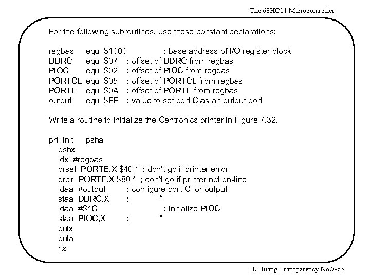
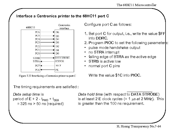 The 68 HC 11 Microcontroller Interface a Centronics printer to the 68 HC 11 port C Configure port C as follows: 1. Set port C for output, i. e. , write the value $FF into DDRC. 2. Program PIOC to set the following parameters: • pulse mode handshake output • no STRA interrupt • falling edge of STRA as the active edge • STRB is active low • normal port C pins Write the value $1 C into PIOC. The timing requirements are satisfied : Data setup time is period of E ÷ 2 - t. PWD + t. DEB = 325 ns > 50 ns (required) Data hold time (with respect to DATA STROBE) is at least 2 E clock cycles (= 1 ms at 2 MHz). This is greater than the 100 ns requirement. H. Huang Transparency No. 7 -64
 The 68 HC 11 Microcontroller For the following subroutines, use these constant declarations: regbas DDRC PIOC PORTCL PORTE output equ equ equ $1000 ; base address of I/O register block $07 ; offset of DDRC from regbas $02 ; offset of PIOC from regbas $05 ; offset of PORTCL from regbas $0 A ; offset of PORTE from regbas $FF ; value to set port C as an output port Write a routine to initialize the Centronics printer in Figure 7. 32. prt_init psha pshx ldx #regbas brset PORTE, X $40 * ; don’t go if printer error brclr PORTE, X $80 * ; don’t go if printer not on-line ldaa #output ; configure port C for output staa DDRC, X ; “ ldaa #$1 C ; initialize PIOC staa PIOC, X ; “ pulx pula rts H. Huang Transparency No. 7 -65
 The 68 HC 11 Microcontroller Write subroutines to print a character and a string using polling method The subroutine prt_char outputs the character in A. prt_char BRCLR PIOC, X $80 * STAA PORTCL, X RTS ; wait until the STAF bit is set to 1 ; print the character in A The subroutine prt_str outputs the string pointed to by index register Y. The index register X contains the base address of the I/O register block. The string is terminated by a NULL character. prt_str next quit PSHA LDAA BEQ JSR INY BRA PULA RTS 0, Y quit prt_char ; get the next character ; is the end of the string? ; print the current character ; move the string pointer next H. Huang Transparency No. 7 -66
 The 68 HC 11 Microcontroller Write subroutines to print a character and a string using interrupt-driven method prt_str 1: enable the interrupt and then wait for the printerrupt until the whole string is printed. prt_char 1: print the character in A and also move the string pointer Y. Set up the interrupt vector table: ORG $FFF 2 FDB prt_char 1 prt_str 1 again BSET CLI LDAA BNE BCLR SEI RTS PIOC, X $40 ; enable STRA interrupt ; “ 0, Y ; wait for printerrupt again ; is this end of the string PIOC, X $40 ; disable STRA interrupt ; disable all interrupt prt_char 1 STAA PORTCL, X INY TSX STY 5, X RTI ; print the character ; move the string pointer ; also update the saved version of Y H. Huang Transparency No. 7 -67
 The 68 HC 11 Microcontroller C Language Version of the Printer Routines void prt_init ( ) { while ((PORTE & 0 x 40) || (!(PORTE & 0 x 80))); DDRC = 0 x. FF; PIOC = 0 x 1 C; } /* polling method version */ void prt_char (char ch) { while (!(PIOC & 0 x 80))); PORTCL = ch; } /* polling method version */ void prt_str (char *ptr) { while(*ptr) { prt_char (*ptr); ptr++; } } H. Huang Transparency No. 7 -68
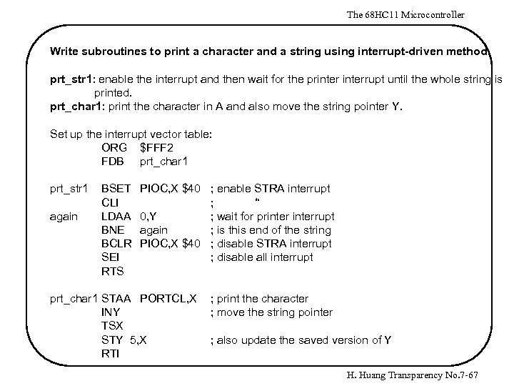
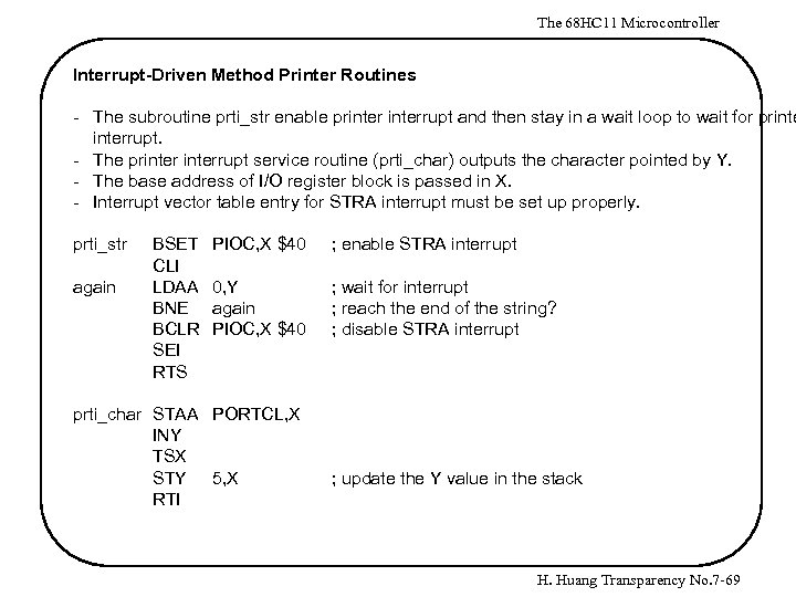 The 68 HC 11 Microcontroller Interrupt-Driven Method Printer Routines - The subroutine prti_str enable printerrupt and then stay in a wait loop to wait for printerrupt. - The printerrupt service routine (prti_char) outputs the character pointed by Y. - The base address of I/O register block is passed in X. - Interrupt vector table entry for STRA interrupt must be set up properly. prti_str again BSET CLI LDAA BNE BCLR SEI RTS PIOC, X $40 ; enable STRA interrupt 0, Y again PIOC, X $40 ; wait for interrupt ; reach the end of the string? ; disable STRA interrupt prti_char STAA PORTCL, X INY TSX STY 5, X RTI ; update the Y value in the stack H. Huang Transparency No. 7 -69
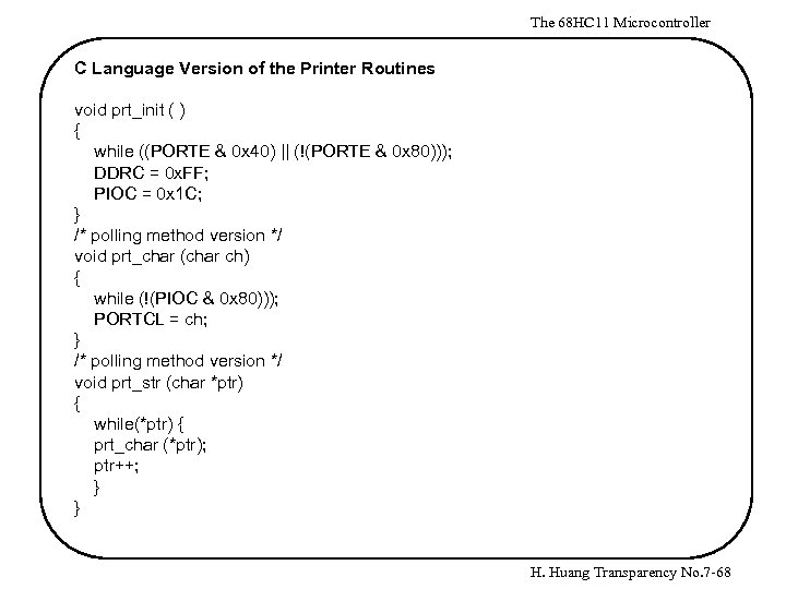
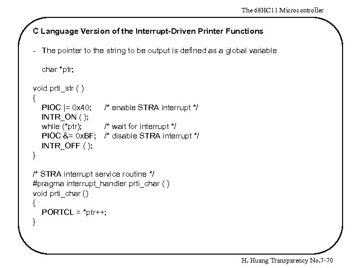 The 68 HC 11 Microcontroller C Language Version of the Interrupt-Driven Printer Functions - The pointer to the string to be output is defined as a global variable char *ptr; void prti_str ( ) { PIOC |= 0 x 40; INTR_ON ( ); while (*ptr); PIOC &= 0 x. BF; INTR_OFF ( ); } /* enable STRA interrupt */ /* wait for interrupt */ /* disable STRA interrupt */ /* STRA interrupt service routine */ #pragma interrupt_handler prti_char ( ) void prti_char () { PORTCL = *ptr++; } H. Huang Transparency No. 7 -70
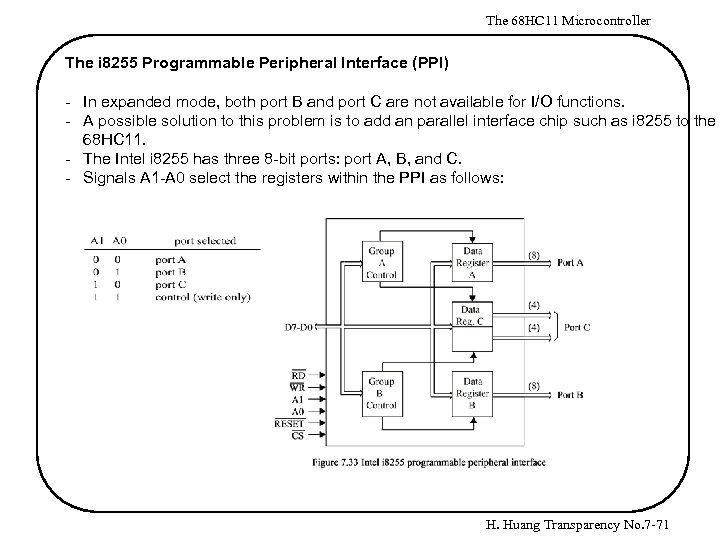 The 68 HC 11 Microcontroller The i 8255 Programmable Peripheral Interface (PPI) - In expanded mode, both port B and port C are not available for I/O functions. - A possible solution to this problem is to add an parallel interface chip such as i 8255 to the 68 HC 11. - The Intel i 8255 has three 8 -bit ports: port A, B, and C. - Signals A 1 -A 0 select the registers within the PPI as follows: H. Huang Transparency No. 7 -71
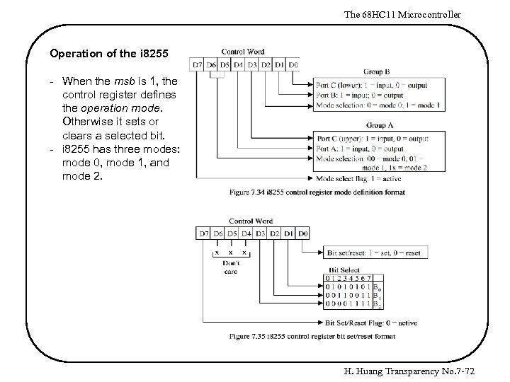 The 68 HC 11 Microcontroller Operation of the i 8255 - When the msb is 1, the control register defines the operation mode. Otherwise it sets or clears a selected bit. - i 8255 has three modes: mode 0, mode 1, and mode 2. H. Huang Transparency No. 7 -72
 The 68 HC 11 Microcontroller Mode 0 (basic input and output) - There are two 8 -bit ports and two 4 -bit ports. Any port can be input or output. Outputs are latched. Inputs are not latched. 16 different input/output configurations are possible in this mode. No handshake is required. Data are simply written into or read from a specified port. H. Huang Transparency No. 7 -73
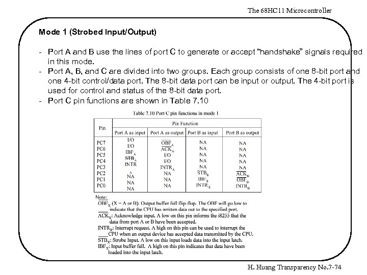 The 68 HC 11 Microcontroller Mode 1 (Strobed Input/Output) - Port A and B use the lines of port C to generate or accept “handshake” signals required in this mode. - Port A, B, and C are divided into two groups. Each group consists of one 8 -bit port and one 4 -bit control/data port. The 8 -bit data port can be input or output. The 4 -bit port is used for control and status of the 8 -bit data port. - Port C pin functions are shown in Table 7. 10 H. Huang Transparency No. 7 -74
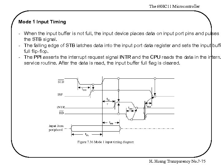 The 68 HC 11 Microcontroller Mode 1 Input Timing - When the input buffer is not full, the input device places data on input port pins and pulses the STB signal. - The falling edge of STB latches data into the input port data register and sets the input buffe full flip-flop. - The PPI asserts the interrupt request signal INTR and the CPU reads the data in the interru service routine. After the data is read, the input buffer full flag is cleared. H. Huang Transparency No. 7 -75
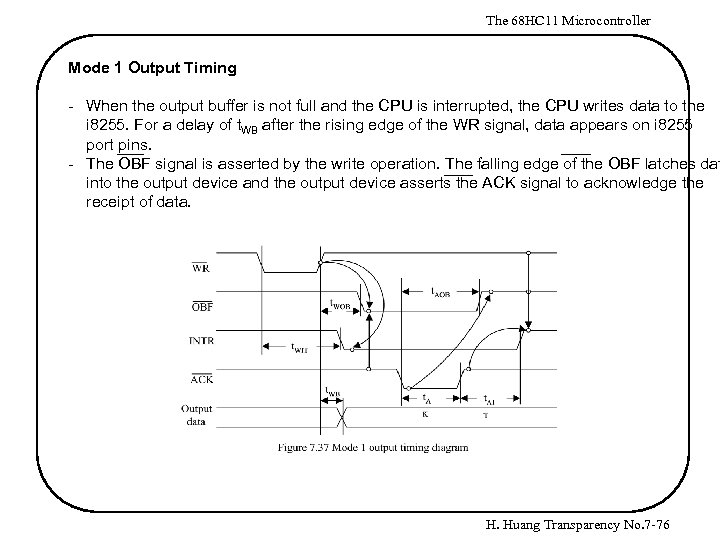 The 68 HC 11 Microcontroller Mode 1 Output Timing - When the output buffer is not full and the CPU is interrupted, the CPU writes data to the i 8255. For a delay of t. WB after the rising edge of the WR signal, data appears on i 8255 port pins. - The OBF signal is asserted by the write operation. The falling edge of the OBF latches dat into the output device and the output device asserts the ACK signal to acknowledge the receipt of data. H. Huang Transparency No. 7 -76
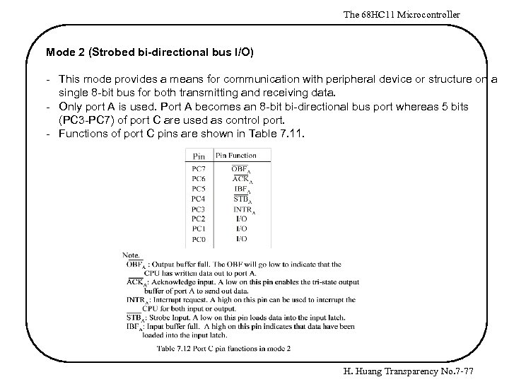 The 68 HC 11 Microcontroller Mode 2 (Strobed bi-directional bus I/O) - This mode provides a means for communication with peripheral device or structure on a single 8 -bit bus for both transmitting and receiving data. - Only port A is used. Port A becomes an 8 -bit bi-directional bus port whereas 5 bits (PC 3 -PC 7) of port C are used as control port. - Functions of port C pins are shown in Table 7. 11. H. Huang Transparency No. 7 -77
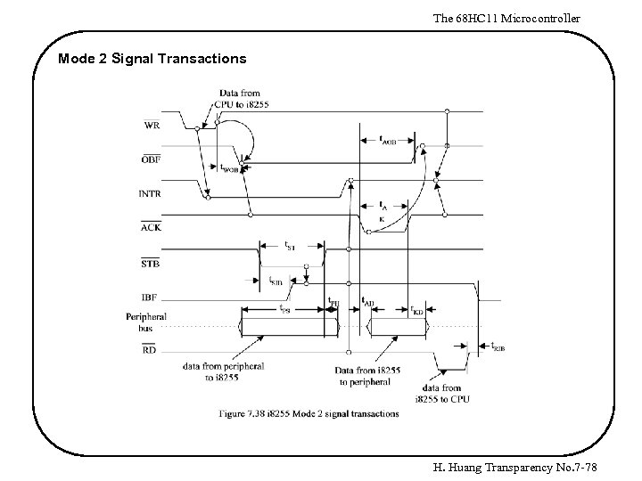 The 68 HC 11 Microcontroller Mode 2 Signal Transactions H. Huang Transparency No. 7 -78
 The 68 HC 11 Microcontroller Mode 2 Data Output Polling approach - The software tests the OBF signal to determine whether the output buffer is empty. If it is the data is written out. - The external circuitry also monitors OBF signal to decide if the microprocessor has sent new data to the i 8255. As soon as OBF is detected to be low, the output device sends ba the ACK signal to remove data from the output buffer. - The low level of the ACK signal causes the OBF signal to go high and enables the threestate output buffer so that data can be read. Interrupt-driven approach - The software first enables the i 8255 interrupt. When the output buffer is empty, it generates an interrupt to the CPU. The CPU outputs a byte to the i 8255 in the interrupt service routine. - The byte written to the i 8255 causes the OBF signal to go low, which informs the output device to latch data. - The output device asserts the ACK signal to acknowledge the receipt of data, which cau the OBF signal to become inactive. H. Huang Transparency No. 7 -79
 The 68 HC 11 Microcontroller Mode 2 Data Input Polling approach - The software tests the IBF signal to determine if data have been strobed into the buffer. - If IBF is low, the input device places data on port A pins and asserts the STB signal to stro data into the input buffer. After this, the IBF signal goes high. - When the user program detects that the IBF signal is high, it reads the data from the input buffer. The IBF signal goes low after the data is read. Interrupt-driven approach - The software first enables the i 8255 to interrupt the CPU. - When the IBF is low, the input device places data on the port pins and asserts the STB sig to strobe data into the input buffer. - After data are strobed into the input buffer, the IBF signal is asserted an interrupt is generated. - The CPU reads the data from the input buffer when executing the interrupt service routine. - Reading data brings the IBF signal to low, which further causes the STB signal to go high. H. Huang Transparency No. 7 -80
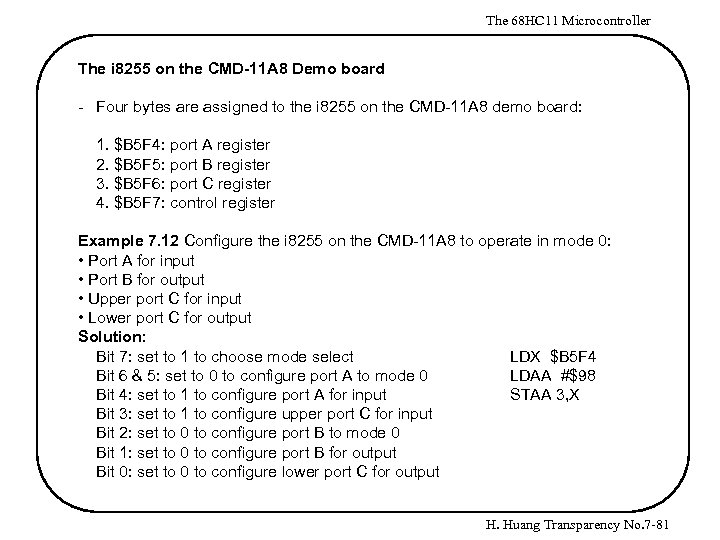 The 68 HC 11 Microcontroller The i 8255 on the CMD-11 A 8 Demo board - Four bytes are assigned to the i 8255 on the CMD-11 A 8 demo board: 1. $B 5 F 4: port A register 2. $B 5 F 5: port B register 3. $B 5 F 6: port C register 4. $B 5 F 7: control register Example 7. 12 Configure the i 8255 on the CMD-11 A 8 to operate in mode 0: • Port A for input • Port B for output • Upper port C for input • Lower port C for output Solution: Bit 7: set to 1 to choose mode select LDX $B 5 F 4 Bit 6 & 5: set to 0 to configure port A to mode 0 LDAA #$98 Bit 4: set to 1 to configure port A for input STAA 3, X Bit 3: set to 1 to configure upper port C for input Bit 2: set to 0 to configure port B to mode 0 Bit 1: set to 0 to configure port B for output Bit 0: set to 0 to configure lower port C for output H. Huang Transparency No. 7 -81
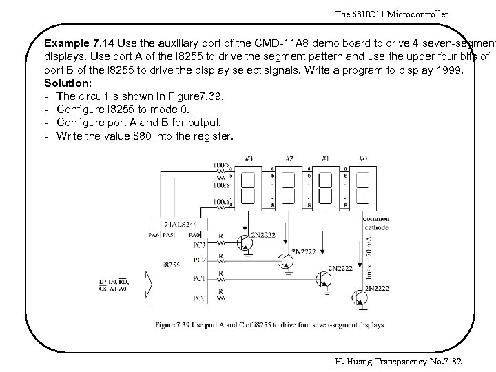 The 68 HC 11 Microcontroller Example 7. 14 Use the auxiliary port of the CMD-11 A 8 demo board to drive 4 seven-segment displays. Use port A of the i 8255 to drive the segment pattern and use the upper four bits of port B of the i 8255 to drive the display select signals. Write a program to display 1999. Solution: - The circuit is shown in Figure 7. 39. - Configure i 8255 to mode 0. - Configure port A and B for output. - Write the value $80 into the register. H. Huang Transparency No. 7 -82
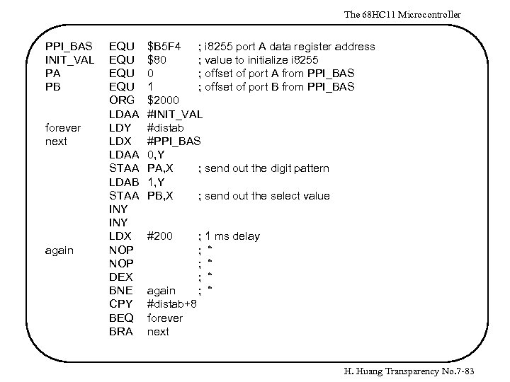 The 68 HC 11 Microcontroller PPI_BAS INIT_VAL PA PB forever next again EQU EQU ORG LDAA LDY LDX LDAA STAA LDAB STAA INY LDX NOP DEX BNE CPY BEQ BRA $B 5 F 4 ; i 8255 port A data register address $80 ; value to initialize i 8255 0 ; offset of port A from PPI_BAS 1 ; offset of port B from PPI_BAS $2000 #INIT_VAL #distab #PPI_BAS 0, Y PA, X ; send out the digit pattern 1, Y PB, X ; send out the select value #200 again #distab+8 forever next ; 1 ms delay ; “ ; “ H. Huang Transparency No. 7 -83
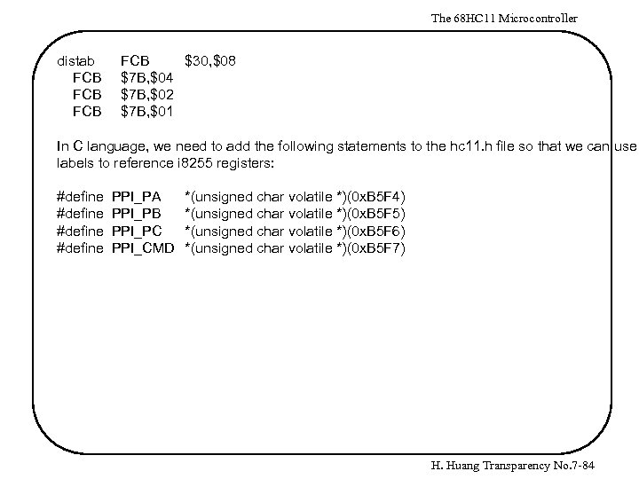 The 68 HC 11 Microcontroller distab FCB FCB $30, $08 $7 B, $04 $7 B, $02 $7 B, $01 In C language, we need to add the following statements to the hc 11. h file so that we can use labels to reference i 8255 registers: #define PPI_PA PPI_PB PPI_PC PPI_CMD *(unsigned char volatile *)(0 x. B 5 F 4) *(unsigned char volatile *)(0 x. B 5 F 5) *(unsigned char volatile *)(0 x. B 5 F 6) *(unsigned char volatile *)(0 x. B 5 F 7) H. Huang Transparency No. 7 -84
![The 68 HC 11 Microcontroller #include <hc 11. h> char distab [4][2] = {{0 The 68 HC 11 Microcontroller #include <hc 11. h> char distab [4][2] = {{0](https://present5.com/presentation/b88ff42555ca36557e91a6bdc64ef4a4/image-85.jpg) The 68 HC 11 Microcontroller #include
The 68 HC 11 Microcontroller #include
 The 68 HC 11 Microcontroller The 68 HC 24 Port Replacement Unit - In the early years of the 68 HC 11, the amount of on-chip EPROM or EEPROM that can be implemented onto the microcontroller chip is very limited. - The software of the target embedded product was to be placed in the on-chip ROM. - During the product development stage, software need to be modified many times. The expanded mode must be chosen and external EPROM must be used so that software can modified and tested. - Ports B and C, which were needed in the final product, were lost in the expanded mode during the product development phase. - The port replacement unit 68 HC 24 was designed to regain ports B and C so that the produ can be evaluated and tested. - After the design had been tested and evaluated to be satisfactory, the software in the external EPROM could be moved into the internal ROM without modification as long as the external EPROM and internal ROM occupied the same memory space. - The signals and an example of the 68 HC 24 application is shown in Figure 7. 38. H. Huang Transparency No. 7 -86
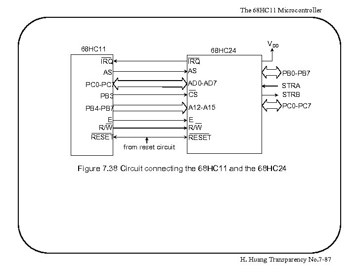 The 68 HC 11 Microcontroller 68 HC 11 68 HC 24 IRQ AS AS AD 0 -AD 7 PC 0 -PC 7 VDD PB 0 -PB 7 CS A 12 -A 15 PB 3 PB 4 -PB 7 E R/W RESET STRA STRB PC 0 -PC 7 E R/W RESET from reset circuit Figure 7. 38 Circuit connecting the 68 HC 11 and the 68 HC 24 H. Huang Transparency No. 7 -87


