2c4ee142f419ad16f867bebac2e06056.ppt
- Количество слайдов: 40
 The 68 HC 11 Microcontroller Chapter 5: Operation Modes and Memory Expansion The 68 HC 11 Microcontroller Han-Way Huang Minnesota State University, Mankato H. Huang Transparency No. 5 -1
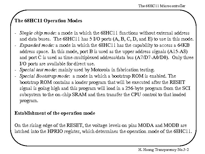 The 68 HC 11 Microcontroller The 68 HC 11 Operation Modes - Single chip mode: a mode in which the 68 HC 11 functions without external address and data buses. The 68 HC 11 has 5 I/O ports (A, B, C, D, and E) to use in this mode. - Expanded mode: a mode in which the 68 HC 11 has the capability to access a 64 KB address space. In this mode, port B is used as the upper address signals (A 15 -A 8) and port C is used as time-multiplexed address/data bus (A 7/D 7 -A 0/D 0). Only three I/O ports are available for direct use. - Special test mode: mainly used by Motorola in fabrication testing. - Special Bootstrap mode: a mode in which a bootstrap ROM is enabled. The bootstrap ROM contains a loader program that will be executed after the RESET signal is going high and this program will load in a 256 -byte program from the SCI subsystem to the on-chip SRAM and then transfer the CPU control to that loaded program. Establishment of the operation mode On the rising edge of the RESET, the voltage levels on pins MODA and MODB are latched into the HPRIO register, which determines the operation mode of the 68 HC 11. H. Huang Transparency No. 5 -2
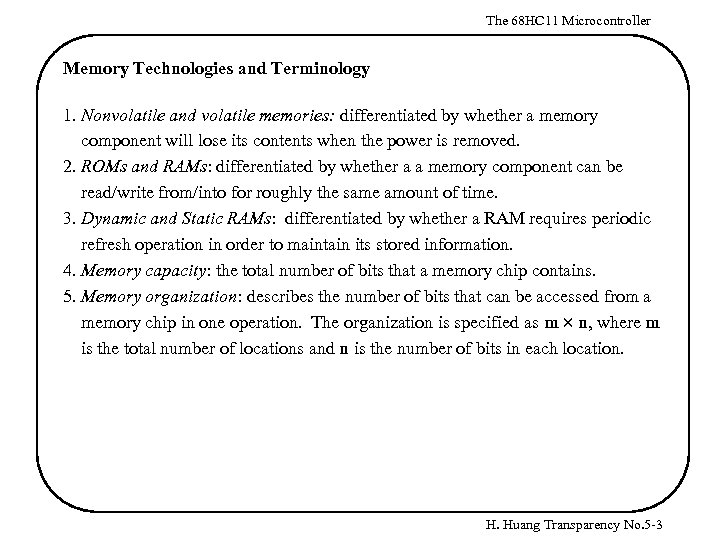 The 68 HC 11 Microcontroller Memory Technologies and Terminology 1. Nonvolatile and volatile memories: differentiated by whether a memory component will lose its contents when the power is removed. 2. ROMs and RAMs: differentiated by whether a a memory component can be read/write from/into for roughly the same amount of time. 3. Dynamic and Static RAMs: differentiated by whether a RAM requires periodic refresh operation in order to maintain its stored information. 4. Memory capacity: the total number of bits that a memory chip contains. 5. Memory organization: describes the number of bits that can be accessed from a memory chip in one operation. The organization is specified as m n, where m is the total number of locations and n is the number of bits in each location. H. Huang Transparency No. 5 -3
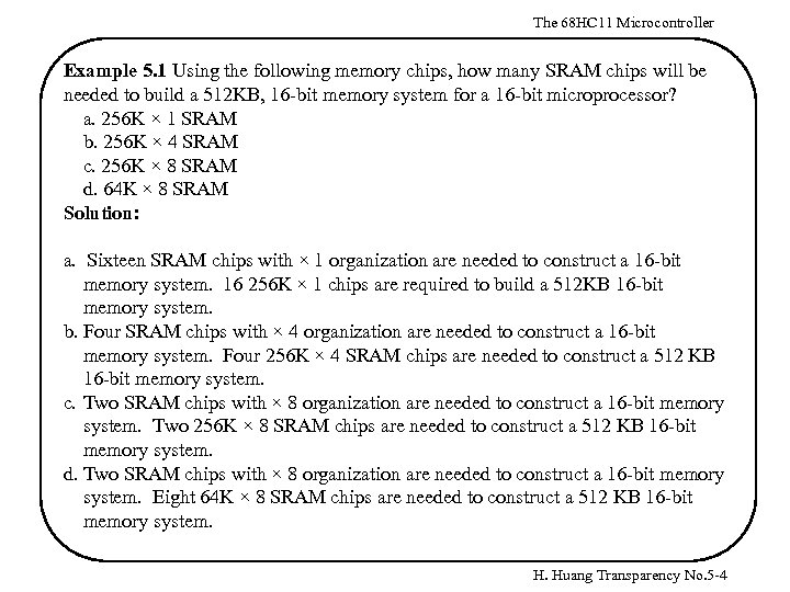 The 68 HC 11 Microcontroller Example 5. 1 Using the following memory chips, how many SRAM chips will be needed to build a 512 KB, 16 -bit memory system for a 16 -bit microprocessor? a. 256 K × 1 SRAM b. 256 K × 4 SRAM c. 256 K × 8 SRAM d. 64 K × 8 SRAM Solution: a. Sixteen SRAM chips with × 1 organization are needed to construct a 16 -bit memory system. 16 256 K × 1 chips are required to build a 512 KB 16 -bit memory system. b. Four SRAM chips with × 4 organization are needed to construct a 16 -bit memory system. Four 256 K × 4 SRAM chips are needed to construct a 512 KB 16 -bit memory system. c. Two SRAM chips with × 8 organization are needed to construct a 16 -bit memory system. Two 256 K × 8 SRAM chips are needed to construct a 512 KB 16 -bit memory system. d. Two SRAM chips with × 8 organization are needed to construct a 16 -bit memory system. Eight 64 K × 8 SRAM chips are needed to construct a 512 KB 16 -bit memory system. H. Huang Transparency No. 5 -4
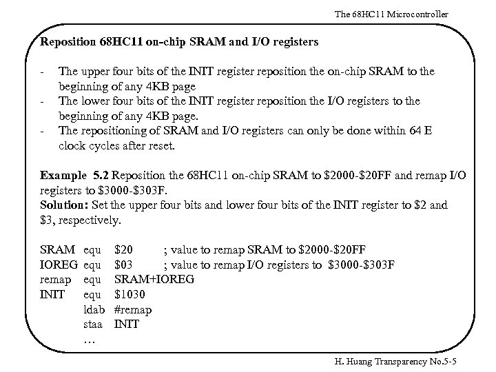 The 68 HC 11 Microcontroller Reposition 68 HC 11 on-chip SRAM and I/O registers - The upper four bits of the INIT register reposition the on-chip SRAM to the beginning of any 4 KB page The lower four bits of the INIT register reposition the I/O registers to the beginning of any 4 KB page. The repositioning of SRAM and I/O registers can only be done within 64 E clock cycles after reset. Example 5. 2 Reposition the 68 HC 11 on-chip SRAM to $2000 -$20 FF and remap I/O registers to $3000 -$303 F. Solution: Set the upper four bits and lower four bits of the INIT register to $2 and $3, respectively. SRAM IOREG remap INIT equ equ ldab staa … $20 ; value to remap SRAM to $2000 -$20 FF $03 ; value to remap I/O registers to $3000 -$303 F SRAM+IOREG $1030 #remap INIT H. Huang Transparency No. 5 -5
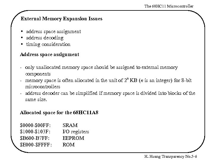 The 68 HC 11 Microcontroller External Memory Expansion Issues • address space assignment • address decoding • timing consideration Address space assignment - only unallocated memory space should be assigned to external memory components - memory space is often allocated in the unit of 2 n KB (n is an integer) for 8 -bit microcontrollers - address decoder can be simplified if memory space is divided into blocks of the same size. Allocated space for the 68 HC 11 A 8 $0000 -$00 FF: $1000 -$103 F: $B 600 -B 7 FF: $E 000 -$FFFF: SRAM I/O registers EEPROM H. Huang Transparency No. 5 -6
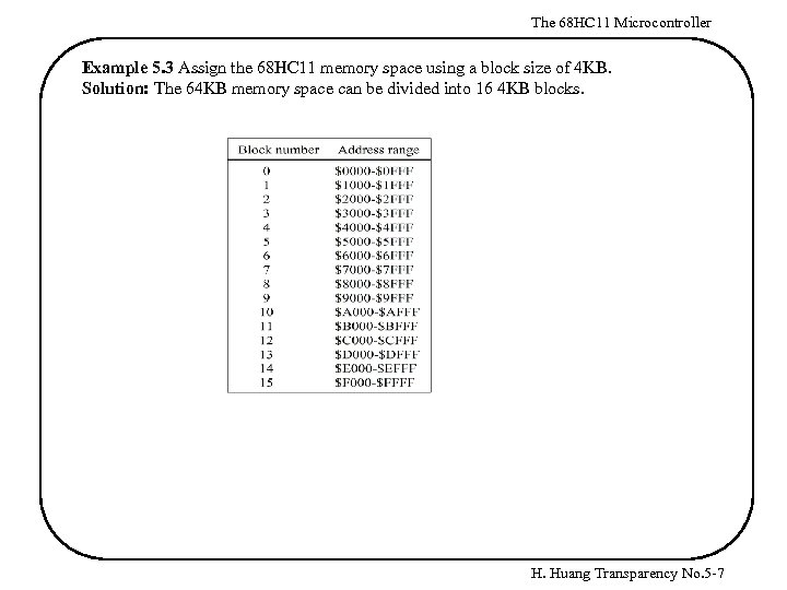 The 68 HC 11 Microcontroller Example 5. 3 Assign the 68 HC 11 memory space using a block size of 4 KB. Solution: The 64 KB memory space can be divided into 16 4 KB blocks. H. Huang Transparency No. 5 -7
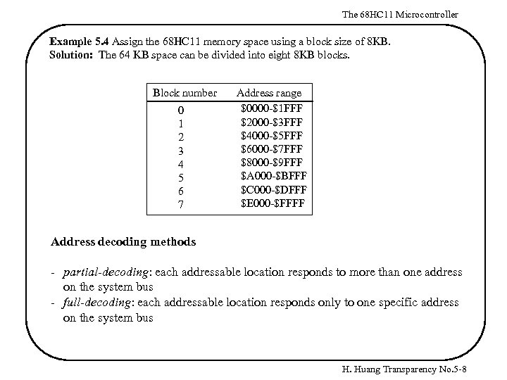 The 68 HC 11 Microcontroller Example 5. 4 Assign the 68 HC 11 memory space using a block size of 8 KB. Solution: The 64 KB space can be divided into eight 8 KB blocks. Block number 0 1 2 3 4 5 6 7 Address range $0000 -$1 FFF $2000 -$3 FFF $4000 -$5 FFF $6000 -$7 FFF $8000 -$9 FFF $A 000 -$BFFF $C 000 -$DFFF $E 000 -$FFFF Address decoding methods - partial-decoding: each addressable location responds to more than one address on the system bus - full-decoding: each addressable location responds only to one specific address on the system bus H. Huang Transparency No. 5 -8
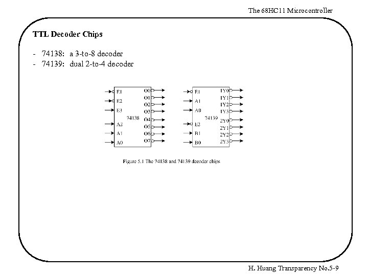 The 68 HC 11 Microcontroller TTL Decoder Chips - 74138: a 3 -to-8 decoder - 74139: dual 2 -to-4 decoder H. Huang Transparency No. 5 -9
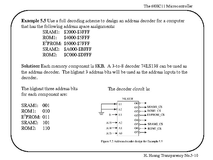 The 68 HC 11 Microcontroller Example 5. 5 Use a full decoding scheme to design an address decoder for a computer that has the following address space assignments: SRAM 1: $2000 -$3 FFF ROM 1: $4000 -$5 FFF E 2 PROM: $6000 -$7 FFF SRAM 2: $A 000 -$BFFF ROM 2: $C 000 -$DFFF Solution: Each memory component is 8 KB. A 3 -to-8 decoder 74 LS 138 can be used as the address decoder. The highest 3 address bits will be used as the address inputs to the decoder. The highest three address bits for each component are: SRAM 1: ROM 1: E 2 PROM: SRAM 2: ROM 2: The decoder circuit is: 001 010 011 101 110 H. Huang Transparency No. 5 -10
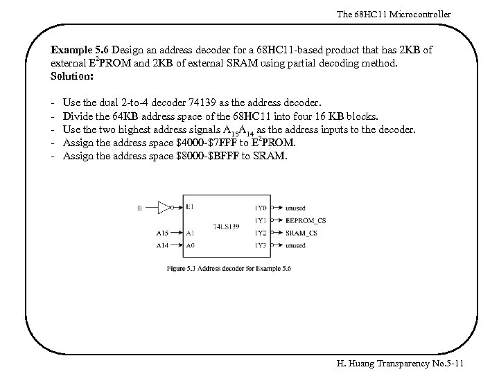 The 68 HC 11 Microcontroller Example 5. 6 Design an address decoder for a 68 HC 11 -based product that has 2 KB of 2 external E PROM and 2 KB of external SRAM using partial decoding method. Solution: - Use the dual 2 -to-4 decoder 74139 as the address decoder. Divide the 64 KB address space of the 68 HC 11 into four 16 KB blocks. Use the two highest address signals A 15 A 14 as the address inputs to the decoder. Assign the address space $4000 -$7 FFF to E 2 PROM. Assign the address space $8000 -$BFFF to SRAM. H. Huang Transparency No. 5 -11
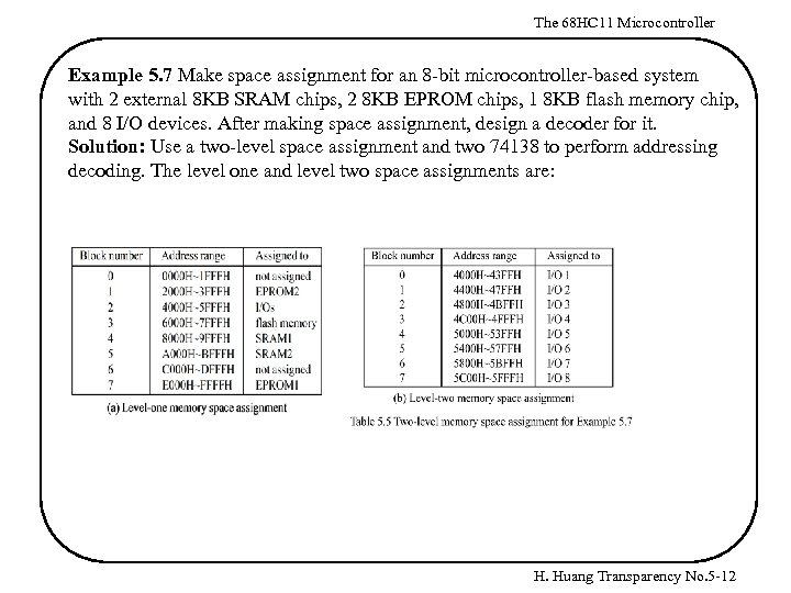 The 68 HC 11 Microcontroller Example 5. 7 Make space assignment for an 8 -bit microcontroller-based system with 2 external 8 KB SRAM chips, 2 8 KB EPROM chips, 1 8 KB flash memory chip, and 8 I/O devices. After making space assignment, design a decoder for it. Solution: Use a two-level space assignment and two 74138 to perform addressing decoding. The level one and level two space assignments are: H. Huang Transparency No. 5 -12
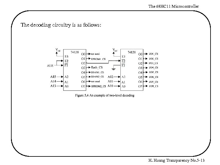 The 68 HC 11 Microcontroller The decoding circuitry is as follows: H. Huang Transparency No. 5 -13
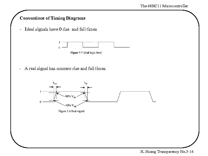 The 68 HC 11 Microcontroller Conventions of Timing Diagrams - Ideal signals have 0 rise and fall times - A real signal has nonzero rise and fall times H. Huang Transparency No. 5 -14
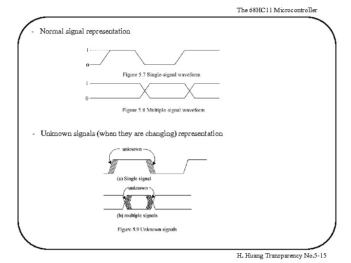 The 68 HC 11 Microcontroller - Normal signal representation - Unknown signals (when they are changing) representation H. Huang Transparency No. 5 -15
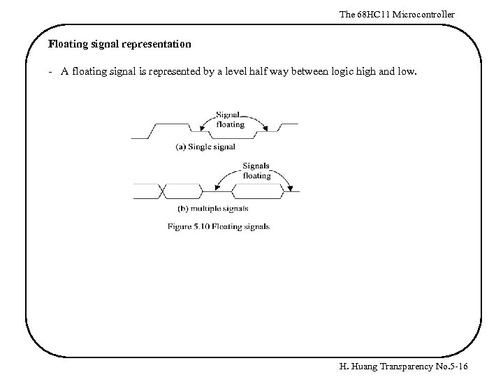 The 68 HC 11 Microcontroller Floating signal representation - A floating signal is represented by a level half way between logic high and low. H. Huang Transparency No. 5 -16
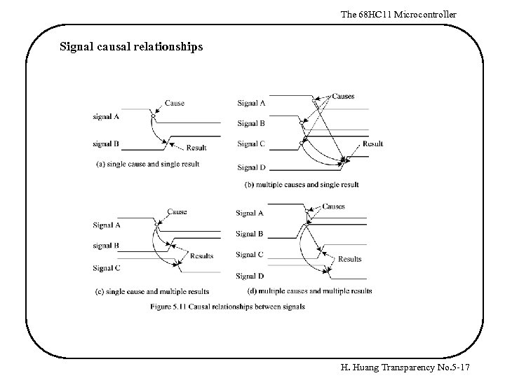 The 68 HC 11 Microcontroller Signal causal relationships H. Huang Transparency No. 5 -17
 The 68 HC 11 Microcontroller The 68 HC 11 Bus Cycle Timing Diagrams - A 68 HC 11 external bus cycle can only be performed in expanded mode and controlled by the E clock signal. - All read and write bus cycles take one E clock cycles to complete. - All timing parameters use 20% and 70% of the power supply voltage as reference points. (Motorola is using this convention) - Most timing parameters are measured relative to the rising and falling edges of the E clock signal. - The phrase before the rising edge of the E clock uses the time when the magnitude of the E clock signal is 0. 2 VDD as a reference point. - The phrase after the rising edge of the E clock uses the time when the magnitude of the E clock signal is 0. 7 VDD as a reference point. - The phrase before the falling edge of the E clock uses the time when the magnitude of the E clock signal is 0. 7 VDD as a reference point. - The phrase after the falling edge of the E clock uses the time when the magnitude of the E clock signal is 0. 2 VDD as a reference point. H. Huang Transparency No. 5 -18
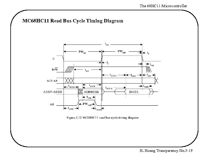 The 68 HC 11 Microcontroller MC 68 HC 11 Read Bus Cycle Timing Diagram H. Huang Transparency No. 5 -19
 The 68 HC 11 Microcontroller For the 2 MHz E clock signal and the 68 HC 11 read bus cycle timing diagram - PWEL is the E clock low pulse width (227 ns) PWEH is the E clock high pulse width (222 ns) A 15 -A 8 and R/W signals are valid t. AV (94 ns) before the rising edge of E clock A 15 -A 8 and R/W signal remain valid for t. AH (30 ns) after the falling edge of E clock A 7 -A 0 and D 7 -D 0 are multiplexed on the same PC 7 -PC 0 pins PC 7 -PC 0 are used as A 7 -A 0 when E clock is low PC 7 -PC 0 are used as D 7 -D 0 when E clock is high A 7 -A 0 are valid t. AVM (86 ns) before the rising edge of E clock Read data must be valid for t. DSR (30 ns) before the falling edge of E clock so that 68 HC 11 can read it correctly Read data must remain valid for t. DHR (0 -83 ns) after the falling edge of E clock so that 68 HC 11 can read it correctly The falling edge of the AS signal is often used by the address latch to latch A 7 -A 0 and A 7 -A 0 remain valid for t. AHL (26 ns) after AS falls Multiplexed address delay is t. MAD (83 ns) after the falling edge of E clock. H. Huang Transparency No. 5 -20
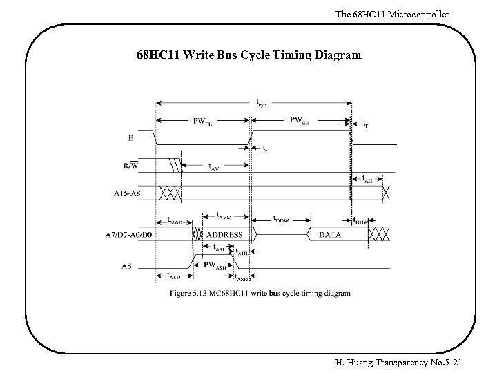 The 68 HC 11 Microcontroller 68 HC 11 Write Bus Cycle Timing Diagram H. Huang Transparency No. 5 -21
 The 68 HC 11 Microcontroller For the 2 MHz E clock and the 68 HC 11 Write bus cycle timing diagram, most signals are identical to those in read bus cycle timing diagram except - the 68 HC 11 drives the data bus when E clock is high - the 68 HC 11 drives D 7 -D 0 t. DDW (128 ns) after the rising edge of the E clock until t. DHW (33 ns) after the falling edge of the E clock H. Huang Transparency No. 5 -22
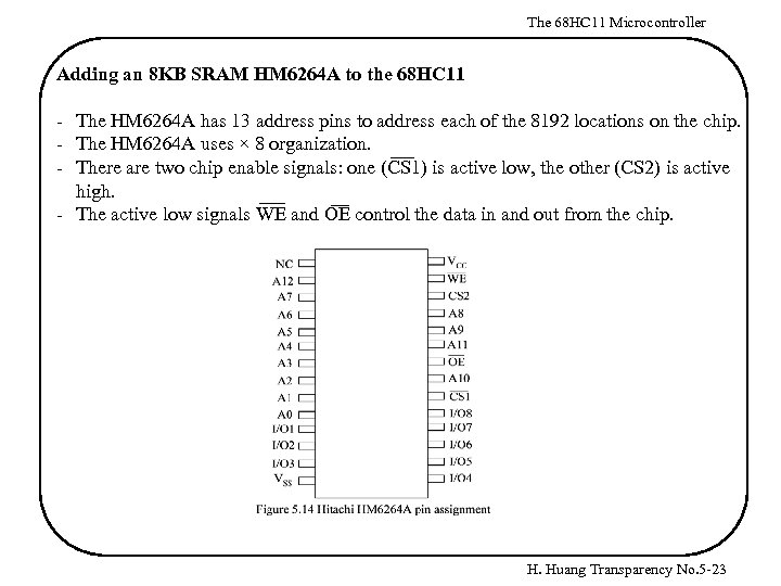 The 68 HC 11 Microcontroller Adding an 8 KB SRAM HM 6264 A to the 68 HC 11 - The HM 6264 A has 13 address pins to address each of the 8192 locations on the chip. - The HM 6264 A uses × 8 organization. - There are two chip enable signals: one (CS 1) is active low, the other (CS 2) is active high. - The active low signals WE and OE control the data in and out from the chip. H. Huang Transparency No. 5 -23
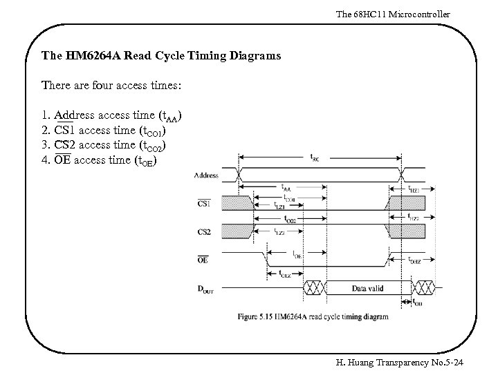 The 68 HC 11 Microcontroller The HM 6264 A Read Cycle Timing Diagrams There are four access times: 1. Address access time (t. AA) 2. CS 1 access time (t. CO 1) 3. CS 2 access time (t. CO 2) 4. OE access time (t. OE) H. Huang Transparency No. 5 -24
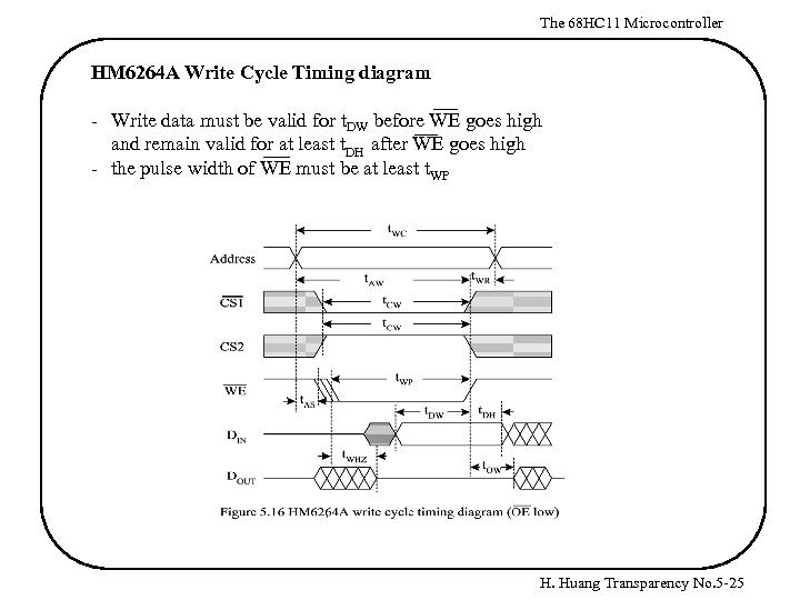 The 68 HC 11 Microcontroller HM 6264 A Write Cycle Timing diagram - Write data must be valid for t. DW before WE goes high and remain valid for at least t. DH after WE goes high - the pulse width of WE must be at least t. WP H. Huang Transparency No. 5 -25
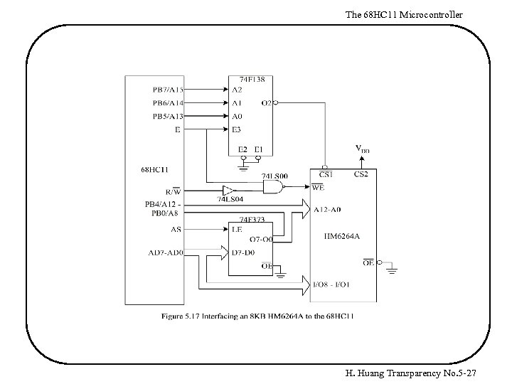
 The 68 HC 11 Microcontroller Interfacing the HM 6264 A-12 with the 2 MHz 68 HC 11 - Address space assigned to the HM 6264 A-12 is $4000 -$5 FFF - The 74 F 138, having a propagation delay of 8 ns, is used as the address decoder - The 74 F 373, having a propagation delay of 11. 5 ns, is used as the low address latch - The WE signal is generated by NANDing the E clock and the inverting copy of R/W. - The NAND gate has a propagation delay of 15 ns. - The inverter that is used to invert the R/W signal has a propagation delay of 15 ns - The circuit connection is in Figure 5. 17 of the next slide H. Huang Transparency No. 5 -26
 The 68 HC 11 Microcontroller H. Huang Transparency No. 5 -27
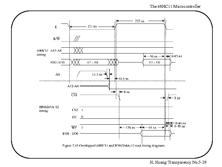
 The 68 HC 11 Microcontroller Read Access Timing Analysis - Timing verification is illustrated using an overlapped 68 HC 11 and HM 6264 A timing diagram in Figure 5. 18. - The time when the data outputs from the HM 6264 A become valid is determined by the last asserted input signal -- CS 1 in this example - A 15 -A 8 are valid 94 ns before E rises - A 7 -A 0 are latched into the 74 F 373 at 41. 5 ns before the rising edge of E clock The lower address signals A 7 -A 0 are latched by the AS signal The AS signal falls to 0. 7 VDD at 53 ns before the rising edge of E clock The 74 F 373 has a propagation of 11. 5 ns A 7 -A 0 is valid at 41. 5 ns (53 - 11. 5) before E rises - WE is high for a read cycle E 3 is the last asserted input signal for 74 F 138 and hence dictates the output valid time O 2 is asserted 8 ns after the rising edge of E clock Data output from the HM 6264 A is valid 128 ns after the rising edge of the E clock or 94 ns (222 - 128) before the rising edge of the E clock -- this satisfies the 68 HC 11 read data setup time (30 ns) H. Huang Transparency No. 5 -28
 The 68 HC 11 Microcontroller H. Huang Transparency No. 5 -29
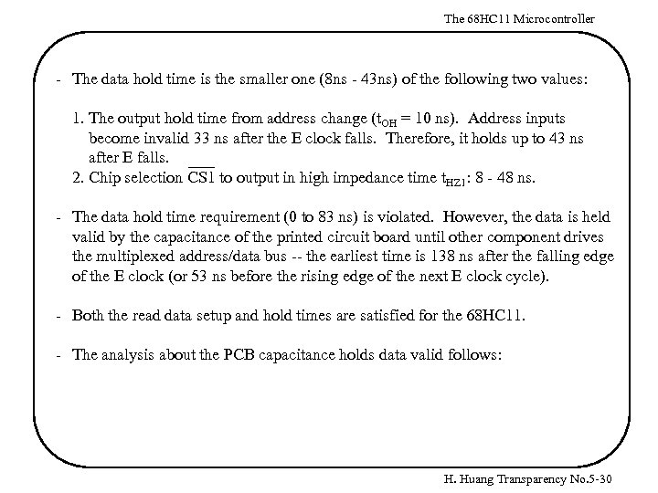 The 68 HC 11 Microcontroller - The data hold time is the smaller one (8 ns - 43 ns) of the following two values: 1. The output hold time from address change (t. OH = 10 ns). Address inputs become invalid 33 ns after the E clock falls. Therefore, it holds up to 43 ns after E falls. 2. Chip selection CS 1 to output in high impedance time t. HZ 1: 8 - 48 ns. - The data hold time requirement (0 to 83 ns) is violated. However, the data is held valid by the capacitance of the printed circuit board until other component drives the multiplexed address/data bus -- the earliest time is 138 ns after the falling edge of the E clock (or 53 ns before the rising edge of the next E clock cycle). - Both the read data setup and hold times are satisfied for the 68 HC 11. - The analysis about the PCB capacitance holds data valid follows: H. Huang Transparency No. 5 -30
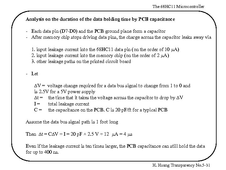 The 68 HC 11 Microcontroller Analysis on the duration of the data holding time by PCB capacitance - Each data pin (D 7 -D 0) and the PCB ground plane form a capacitor - After memory chip stops driving data pins, the charge across the capacitor leaks away via 1. input leakage current into the 68 HC 11 data pin (on the order of 10 m. A) 2. input leakage current into the memory chip (on the order of 2 m. A) 3. other leakage paths on the printed circuit board - Let DV = voltage change required for a data bus signal to change from 1 to 0 and is 2. 5 V for a 5 V power supply Dt = the time that it takes the voltage across the capacitor to drop by DV I= total leakage current C = the capacitance on the PCB. C is 20 p. F/ft for a typical PCB Assume the data bus signal path is 1 foot long Then Dt = CDV ÷ I = 20 p. F × 2. 5 V ÷ 12 m. A = 4 ms Even if the leakage current is ten times larger, the PCB capacitance can still hold the data for up to 400 ns. H. Huang Transparency No. 5 -31
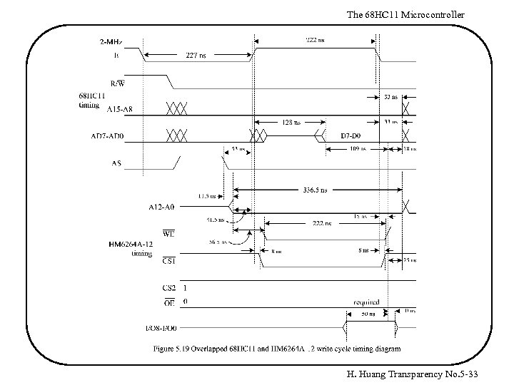
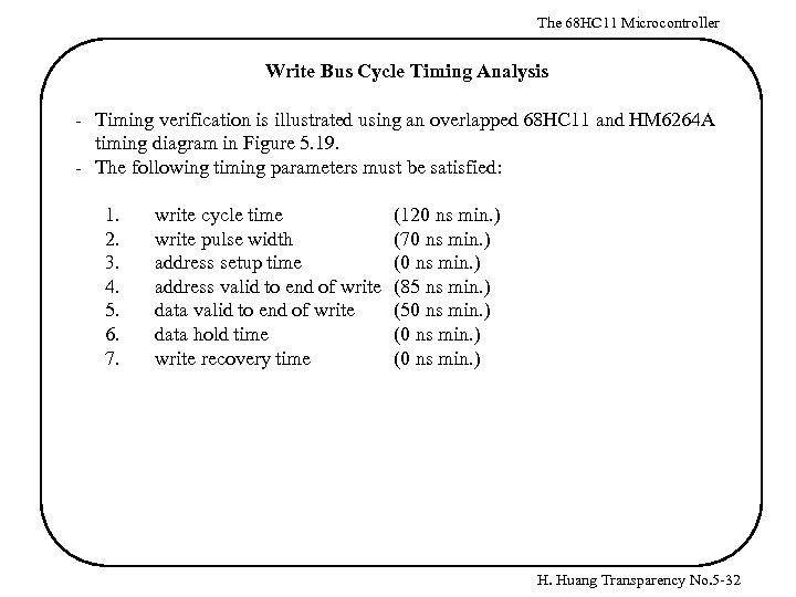 The 68 HC 11 Microcontroller Write Bus Cycle Timing Analysis - Timing verification is illustrated using an overlapped 68 HC 11 and HM 6264 A timing diagram in Figure 5. 19. - The following timing parameters must be satisfied: 1. 2. 3. 4. 5. 6. 7. write cycle time write pulse width address setup time address valid to end of write data hold time write recovery time (120 ns min. ) (70 ns min. ) (85 ns min. ) (50 ns min. ) (0 ns min. ) H. Huang Transparency No. 5 -32
 The 68 HC 11 Microcontroller H. Huang Transparency No. 5 -33
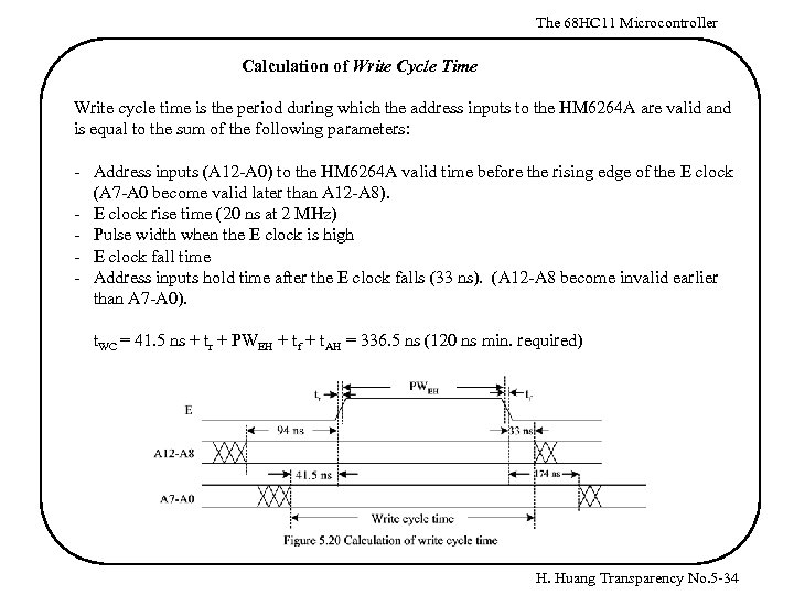 The 68 HC 11 Microcontroller Calculation of Write Cycle Time Write cycle time is the period during which the address inputs to the HM 6264 A are valid and is equal to the sum of the following parameters: - Address inputs (A 12 -A 0) to the HM 6264 A valid time before the rising edge of the E clock (A 7 -A 0 become valid later than A 12 -A 8). - E clock rise time (20 ns at 2 MHz) - Pulse width when the E clock is high - E clock fall time - Address inputs hold time after the E clock falls (33 ns). (A 12 -A 8 become invalid earlier than A 7 -A 0). t. WC = 41. 5 ns + tr + PWEH + tf + t. AH = 336. 5 ns (120 ns min. required) H. Huang Transparency No. 5 -34
 The 68 HC 11 Microcontroller Calculation of Write Pulse Width (WE) Since the WE signal is the NAND function of the R/W and E clock, the width is equal to the high pulse width of the E clock and is equal to 222 ns (70 ns is required). H. Huang Transparency No. 5 -35
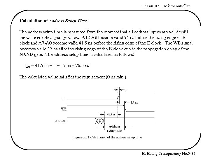 The 68 HC 11 Microcontroller Calculation of Address Setup Time The address setup time is measured from the moment that all address inputs are valid until the write enable signal goes low. A 12 -A 8 become valid 94 ns before the rising edge of E clock and A 7 -A 0 become valid 41. 5 ns before the rising edge of the E clock. The WE signal becomes valid 15 ns after the rising edge of the E clock due to the propagation delay of the NAND gate. The address setup time is calculated as follows: t. AS = 41. 5 ns + tr + 15 ns = 76. 5 ns The calculated value satisfies the requirement (0 ns min. ). H. Huang Transparency No. 5 -36
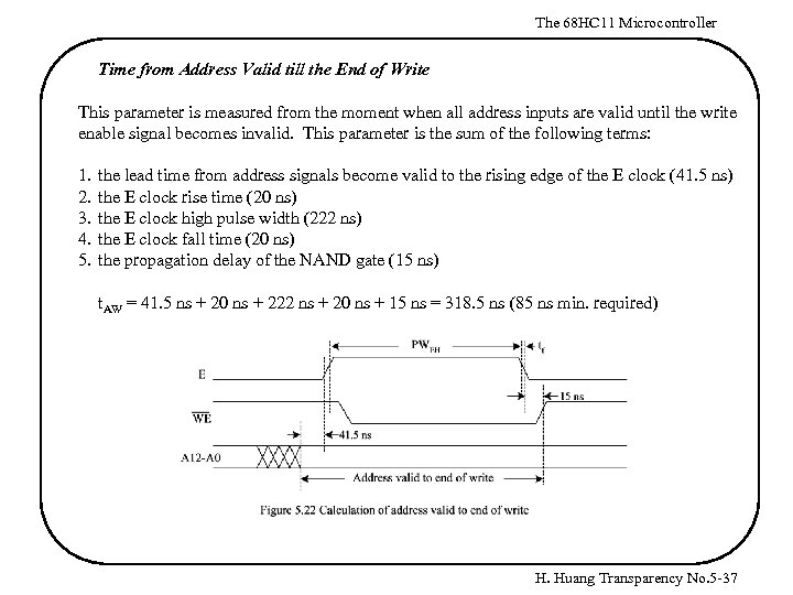 The 68 HC 11 Microcontroller Time from Address Valid till the End of Write This parameter is measured from the moment when all address inputs are valid until the write enable signal becomes invalid. This parameter is the sum of the following terms: 1. 2. 3. 4. 5. the lead time from address signals become valid to the rising edge of the E clock (41. 5 ns) the E clock rise time (20 ns) the E clock high pulse width (222 ns) the E clock fall time (20 ns) the propagation delay of the NAND gate (15 ns) t. AW = 41. 5 ns + 20 ns + 222 ns + 20 ns + 15 ns = 318. 5 ns (85 ns min. required) H. Huang Transparency No. 5 -37
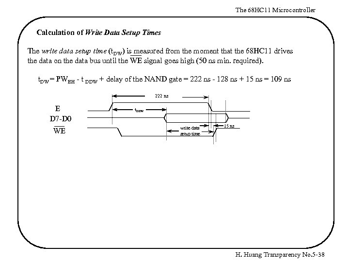 The 68 HC 11 Microcontroller Calculation of Write Data Setup Times The write data setup time (t. DW) is measured from the moment that the 68 HC 11 drives the data on the data bus until the WE signal goes high (50 ns min. required). t. DW = PWEH - t DDW + delay of the NAND gate = 222 ns - 128 ns + 15 ns = 109 ns 222 ns E D 7 -D 0 WE t. DDW write data setup time 15 ns H. Huang Transparency No. 5 -38
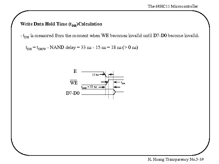 The 68 HC 11 Microcontroller Write Data Hold Time (t. DH)Calculation - t. DH is measured from the moment when WE becomes invalid until D 7 -D 0 become invalid. t. DH = t. DHW - NAND delay = 33 ns - 15 ns = 18 ns (> 0 ns) E WE 15 ns t. DHW = 33 ns D 7 -D 0 H. Huang Transparency No. 5 -39
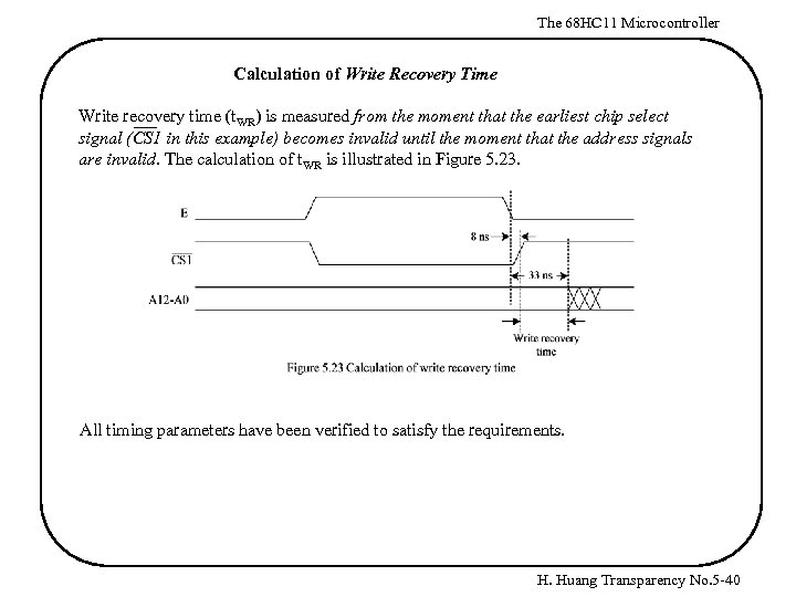 The 68 HC 11 Microcontroller Calculation of Write Recovery Time Write recovery time (t. WR) is measured from the moment that the earliest chip select signal (CS 1 in this example) becomes invalid until the moment that the address signals are invalid. The calculation of t. WR is illustrated in Figure 5. 23. All timing parameters have been verified to satisfy the requirements. H. Huang Transparency No. 5 -40


