 Testing an Inkjet Printer for Use in MEMS Fabrication Marvin Cruz Home Institution: University of California, Santa Cruz Principal Investigator: Joel Kubby, Ph. D Research Mentor: Oscar Azucena Center for Adaptive Optics University of California, Santa Cruz 1
 Outline 1. 2. 3. 4. Introduction to MEMS Project Description Process and General Workflow Data Analysis and Results 2
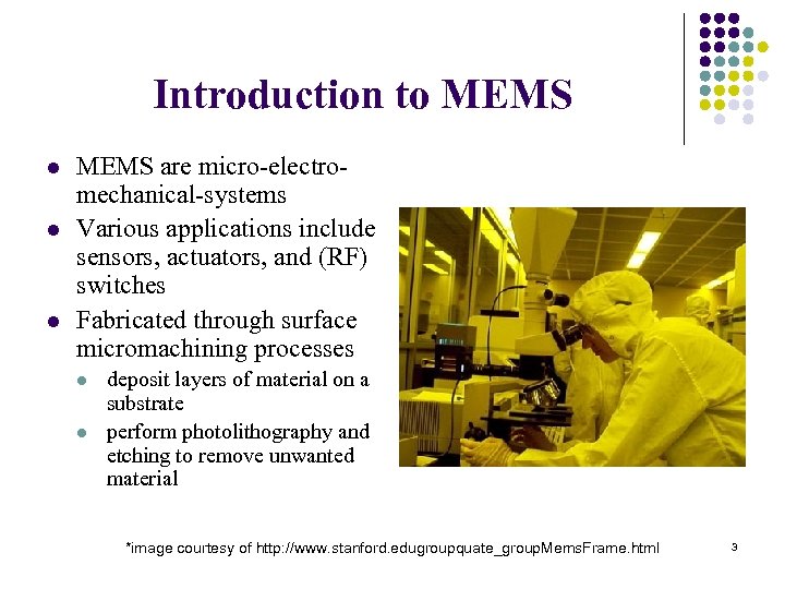 Introduction to MEMS l l l MEMS are micro-electromechanical-systems Various applications include sensors, actuators, and (RF) switches Fabricated through surface micromachining processes l l deposit layers of material on a substrate perform photolithography and etching to remove unwanted material *image courtesy of http: //www. stanford. edugroupquate_group. Mems. Frame. html 3
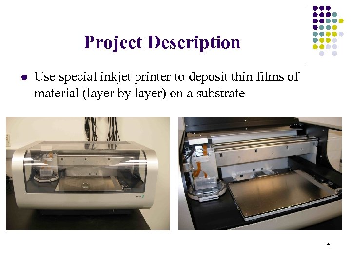 Project Description l Use special inkjet printer to deposit thin films of material (layer by layer) on a substrate 4
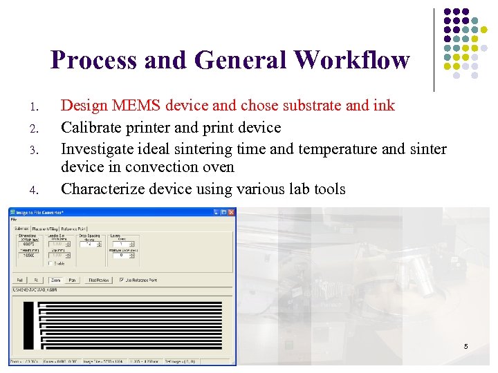 Process and General Workflow 1. 2. 3. 4. Design MEMS device and chose substrate and ink Calibrate printer and print device Investigate ideal sintering time and temperature and sinter device in convection oven Characterize device using various lab tools 5
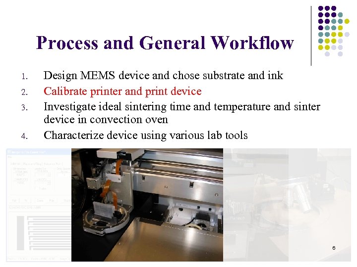 Process and General Workflow 1. 2. 3. 4. Design MEMS device and chose substrate and ink Calibrate printer and print device Investigate ideal sintering time and temperature and sinter device in convection oven Characterize device using various lab tools 6
 Process and General Workflow 1. 2. 3. 4. Design MEMS device and chose substrate and ink Calibrate printer and print device Investigate ideal sintering time and temperature and sinter device in convection oven Characterize device using various lab tools 7
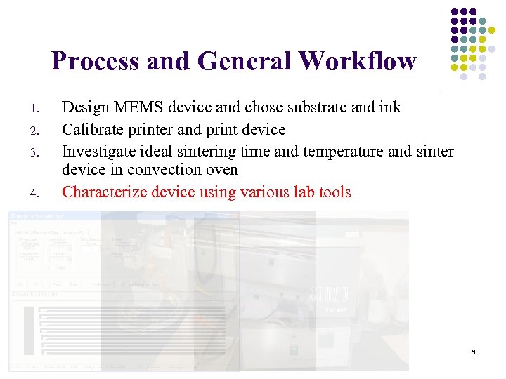 Process and General Workflow 1. 2. 3. 4. Design MEMS device and chose substrate and ink Calibrate printer and print device Investigate ideal sintering time and temperature and sinter device in convection oven Characterize device using various lab tools 8
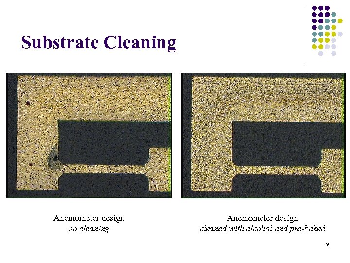 Substrate Cleaning Anemometer design no cleaning Anemometer design cleaned with alcohol and pre-baked 9
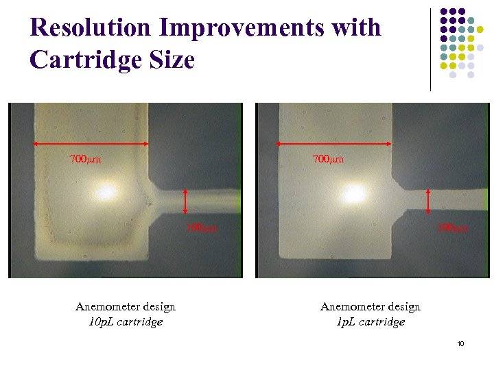 Resolution Improvements with Cartridge Size 700µm 100µm Anemometer design 10 p. L cartridge 100µm Anemometer design 1 p. L cartridge 10
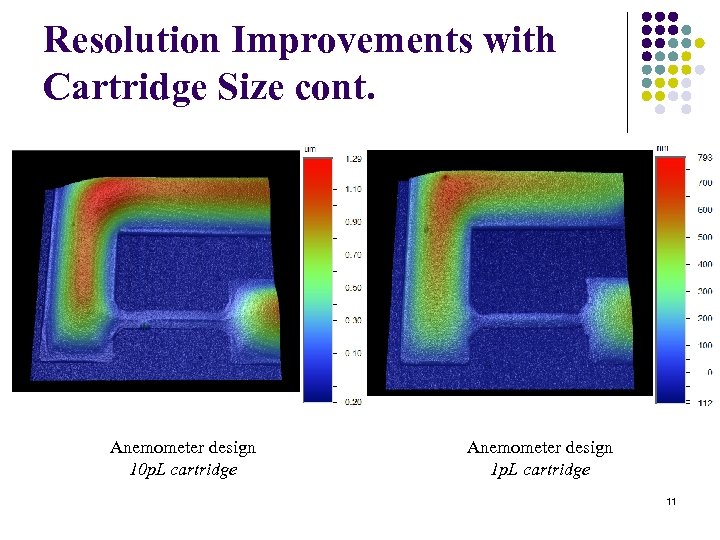 Resolution Improvements with Cartridge Size cont. Anemometer design 10 p. L cartridge Anemometer design 1 p. L cartridge 11
 Conductivity and Sintering Temperature 12
 Future Work l l Continue testing other substrates and observe relevant topography characteristics and measure conductivity Extend printing to include more complex, multi-layered devices 13
 Acknowledgements l l l l Joel Kubby Oscar Azucena Bautista Fernández Darwin Fernandez Lynne Raschke Hilary O’Bryan Lisa Hunter faculty, friends, and fellow interns from the Cf. AO This project is supported by the National Science Foundation Science and Technology Center for Adaptive Optics, managed by the University of California at Santa Cruz under cooperative agreement No. AST - 9876783 14