TEM_theory_KZ.pptx
- Количество слайдов: 81
 TEM Transmision Electrom Microscope Construction and Application Prof. dr habil. ing. Włodzimierz Dudziński
 Plan of presentation • • Introduction, Selected parts of construction, Electron gun, Lenses, Specimen holder, Image registration, Detectors – different types
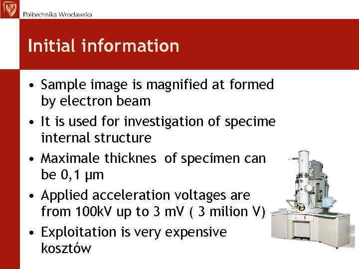 Initial information • Sample image is magnified at formed by electron beam • It is used for investigation of specime internal structure • Maximale thicknes of specimen can be 0, 1 µm • Applied acceleration voltages are from 100 k. V up to 3 m. V ( 3 milion V) • Exploitation is very expensive kosztów
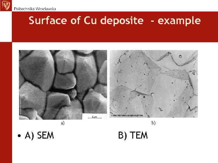 Surface of Cu deposite - example • A) SEM B) TEM
 Application • Presentation of specimens internal structure • Images are not coloured • Application at materials science, biology, medicine and geology • Microstructure, crystalographic orientation, atomic resolution, chemical composition of different phases can be investigated (HREM, EDX, EELS) • 3 D imaging of specimen is possible (STEM)
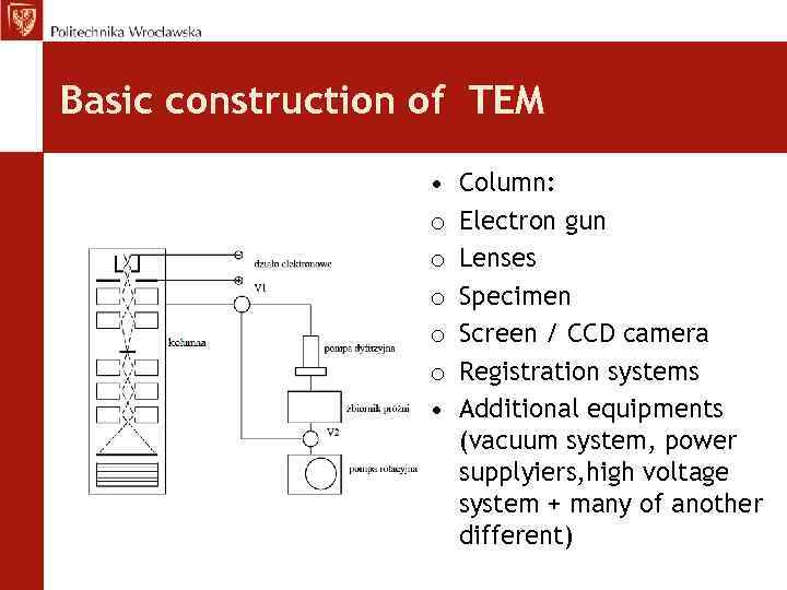 Basic construction of TEM • o o o • Column: Electron gun Lenses Specimen Screen / CCD camera Registration systems Additional equipments (vacuum system, power supplyiers, high voltage system + many of another different)
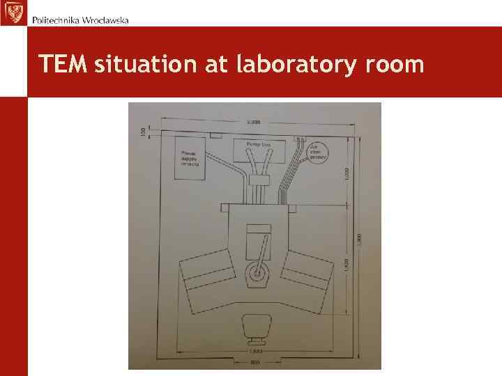 TEM situation at laboratory room
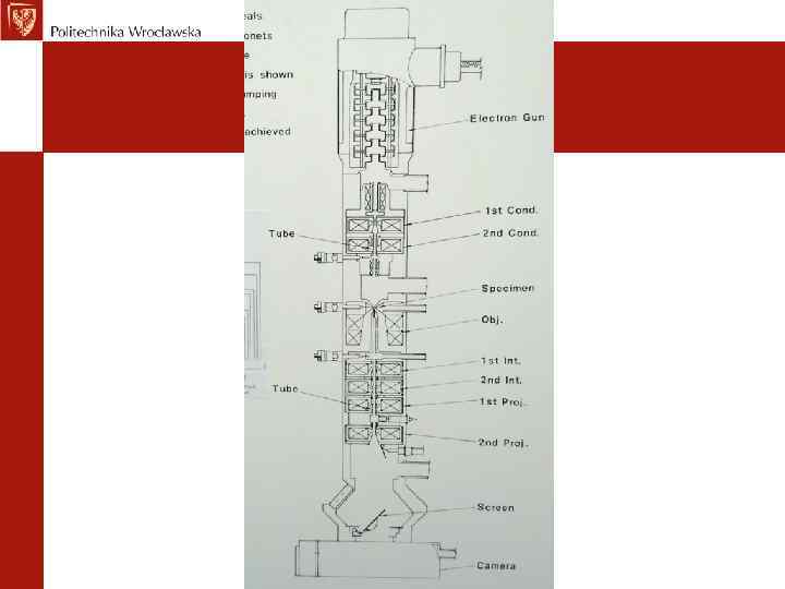
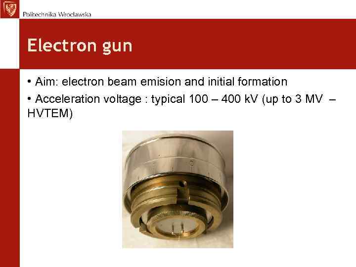 Electron gun • Aim: electron beam emision and initial formation • Acceleration voltage : typical 100 – 400 k. V (up to 3 MV – HVTEM)
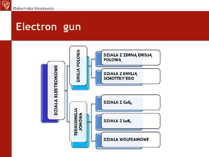 Electron gun
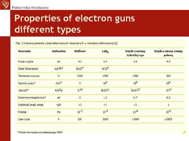 Properties of electron guns different types
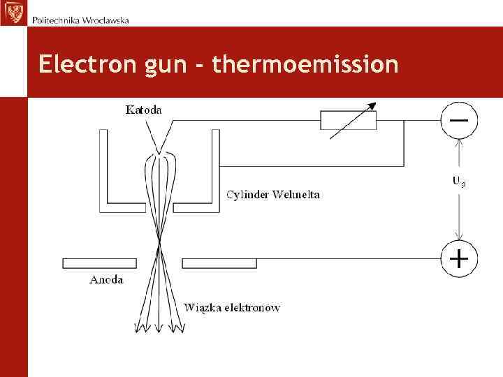 Electron gun - thermoemission
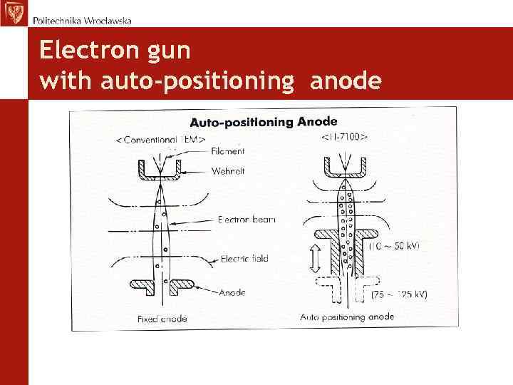 Electron gun with auto-positioning anode
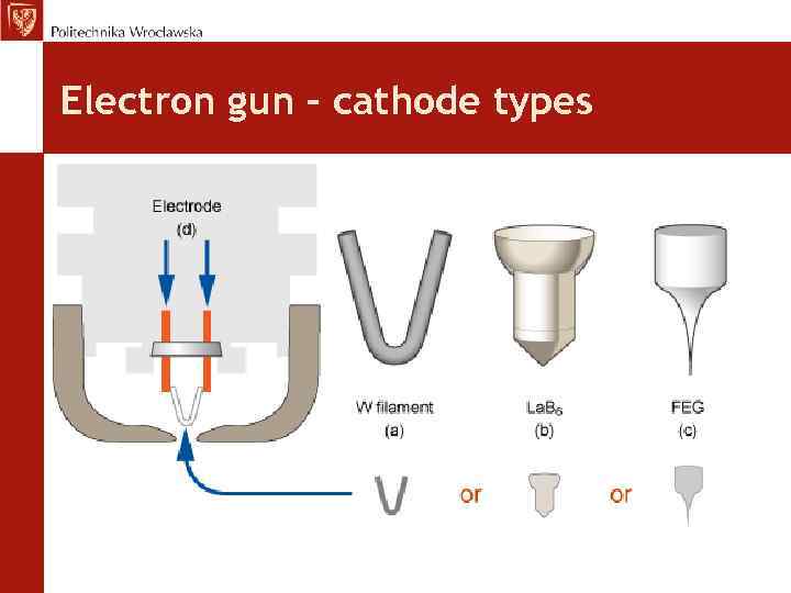 Electron gun – cathode types
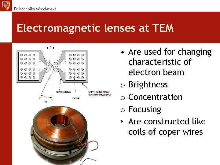 Electromagnetic lenses at TEM • Are used for changing characteristic of electron beam o Brightness o Concentration o Focusing • Are constructed like coils of coper wires
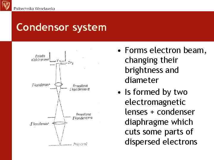 Condensor system • Forms electron beam, changing their brightness and diameter • Is formed by two electromagnetic lenses + condenser diaphragme which cuts some parts of dispersed electrons
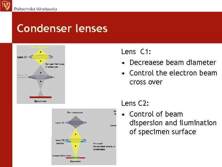 Condenser lenses Lens C 1: • Decreaese beam diameter • Control the electron beam cross over Lens C 2: • Control of beam dispersion and ilumination of specimen surface
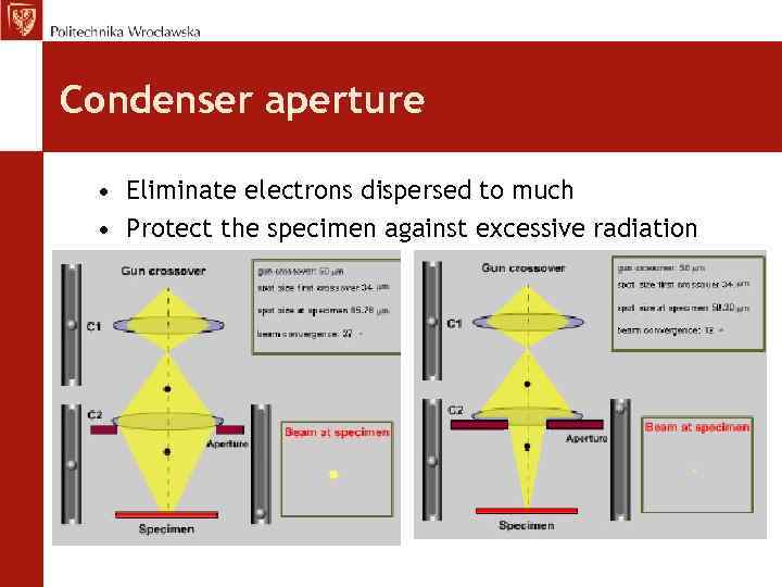 Condenser aperture • Eliminate electrons dispersed to much • Protect the specimen against excessive radiation
 Specimen chamber • Very high precission of specimen movement, along X, Y and Z direction (up to 1µm). Very high stabilisation is necessary • Additionally mounted equipment: - Goniometer – allows specimen tilting and rotation - Heating device – on line structure observation during heating time - Cooling device – used for biological specimens and protections against contamination – liquid nitrogen is applied - X-ray, EELS or Auger spectrometers (STEM)
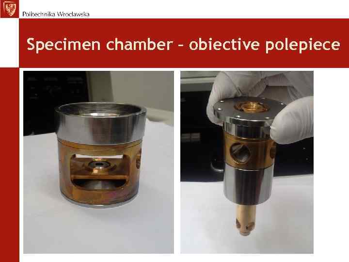 Specimen chamber – obiective polepiece
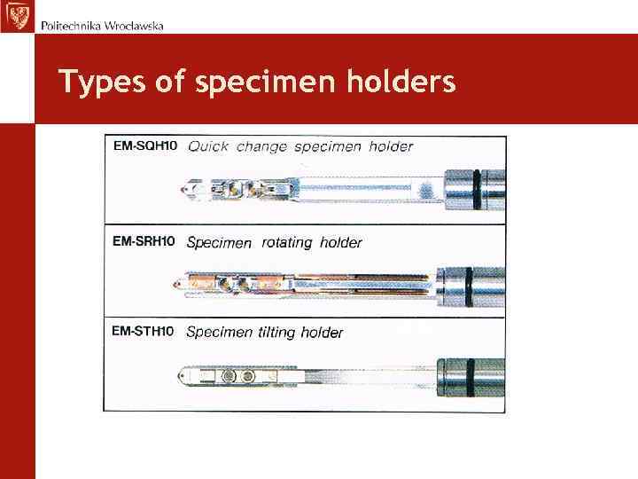 Types of specimen holders
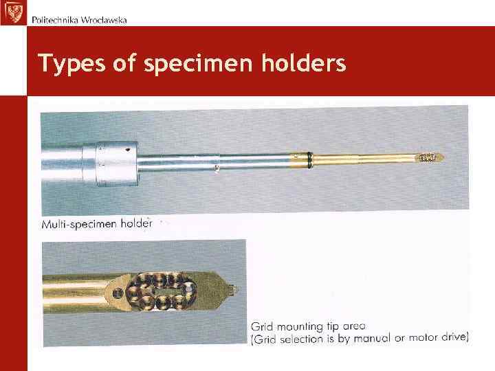 Types of specimen holders
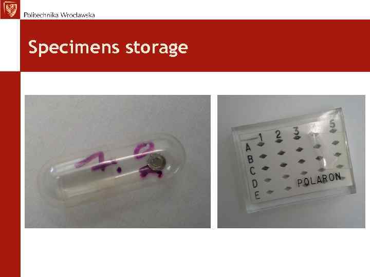 Specimens storage
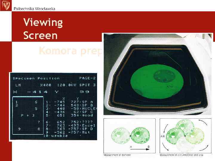 Viewing Screen Komora preparatu
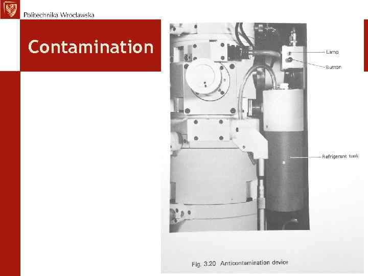
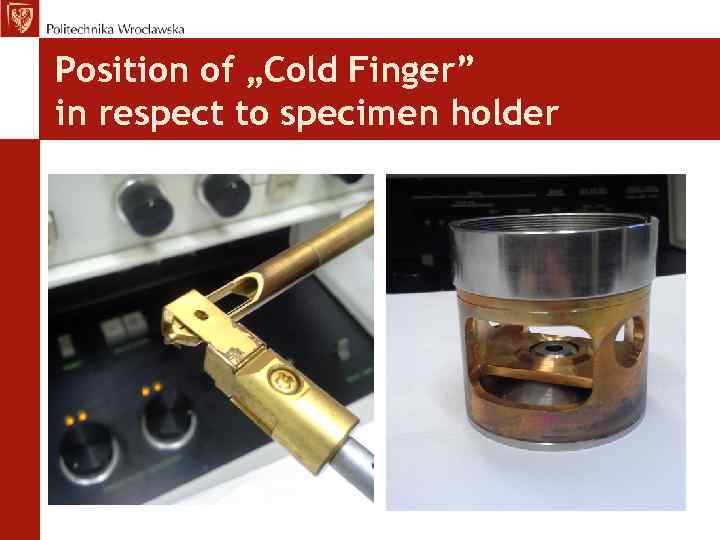
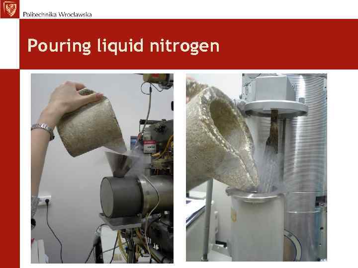
 Contamination Negative phenomenon – the rest of silicon oil vapeurs deriving from cacuum pumps are sedimented on the specimen surface and borders of apertures. This phenomenon can heavy decrease contrast and resolution of images. Protection: • Instalation of anti contamination device inside TEM column – i. e. ring or „cold fingers” sourrounded specimen - cooled by liquid nitrogene • Increasing of vacuum quality by application „Cold Trap” and „oil free” pomps like: Ion Getter Pump (IGP) or Turbo Molecular Pump (TMP).
 Contamination
 Position of „Cold Finger” in respect to specimen holder
 Pouring liquid nitrogen
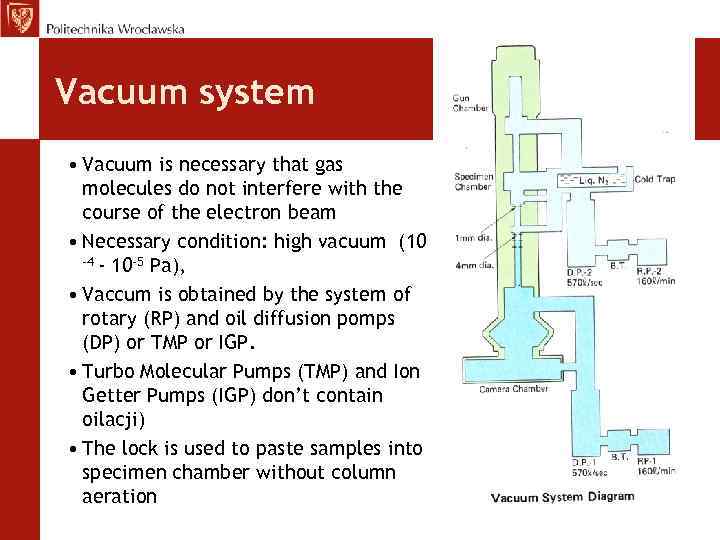 Vacuum system • Vacuum is necessary that gas molecules do not interfere with the course of the electron beam • Necessary condition: high vacuum (10 -4 - 10 -5 Pa), • Vaccum is obtained by the system of rotary (RP) and oil diffusion pomps (DP) or TMP or IGP. • Turbo Molecular Pumps (TMP) and Ion Getter Pumps (IGP) don’t contain oilacji) • The lock is used to paste samples into specimen chamber without column aeration
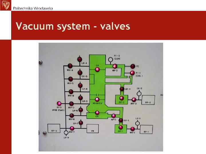 Vacuum system - valves
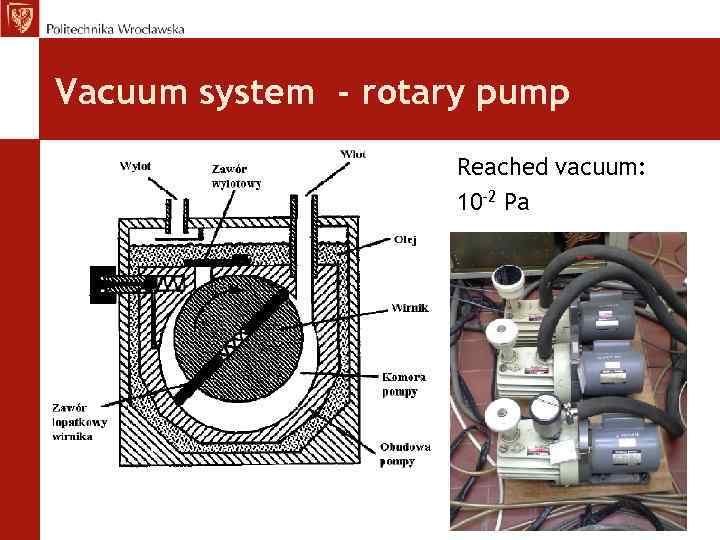 Vacuum system - rotary pump Reached vacuum: 10 -2 Pa
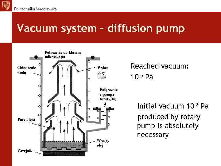 Vacuum system – diffusion pump Reached vacuum: 10 -5 Pa Initial vacuum 10 -2 Pa produced by rotary pump is absolutely necessary
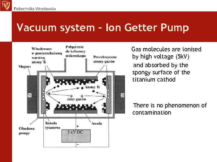 Vacuum system – Ion Getter Pump Gas molecules are ionised by high voltage (5 k. V) and absorbed by the spongy surface of the titanium cathod B There is no phenomenon of contamination
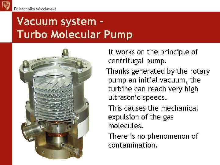 Vacuum system – Turbo Molecular Pump It works on the principle of centrifugal pump. Thanks generated by the rotary pump an initial vacuum, the turbine can reach very high ultrasonic speeds. This causes the mechanical expulsion of the gas molecules. There is no phenomenon of contamination.
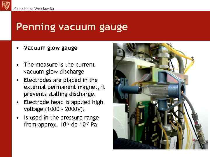 Penning vacuum gauge • Vacuum glow gauge • The measure is the current vacuum glow discharge • Electrodes are placed in the external permanent magnet, it prevents stalling discharge. • Electrode head is applied high voltage (1000 - 2000 V). • Is used in the pressure range from approx. 10 -2 do 10 -7 Pa
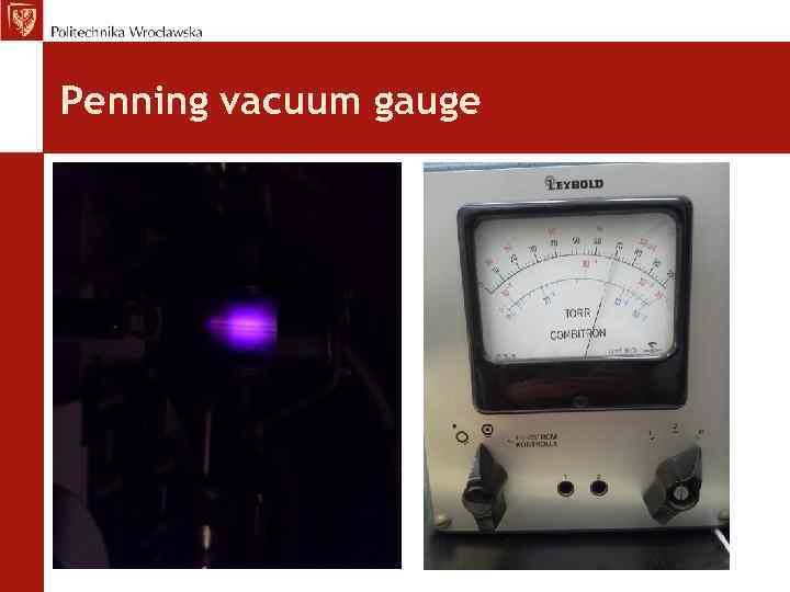 Penning vacuum gauge
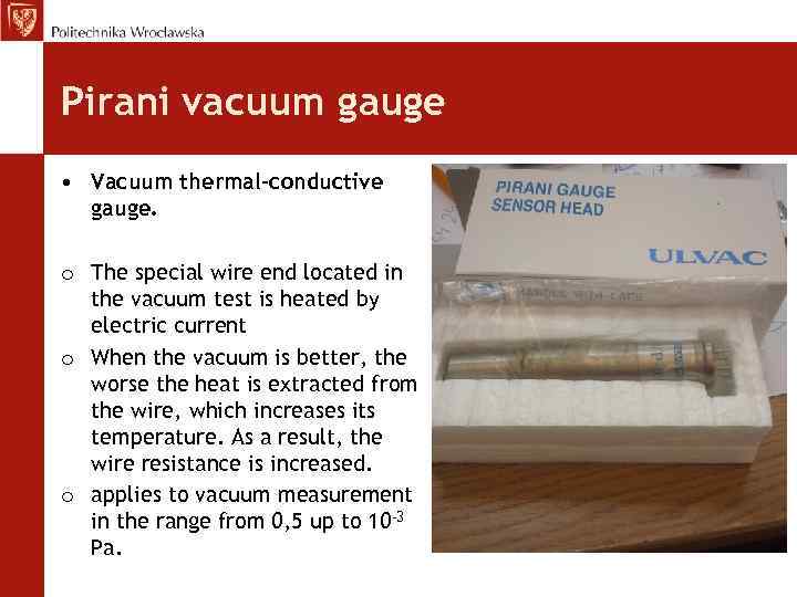 Pirani vacuum gauge • Vacuum thermal-conductive gauge. o The special wire end located in the vacuum test is heated by electric current o When the vacuum is better, the worse the heat is extracted from the wire, which increases its temperature. As a result, the wire resistance is increased. o applies to vacuum measurement in the range from 0, 5 up to 10 -3 Pa.
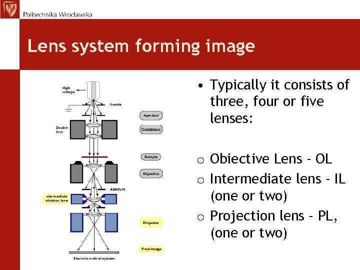 Lens system forming image • Typically it consists of three, four or five lenses: o Obiective Lens - OL o Intermediate lens - IL (one or two) o Projection lens - PL, (one or two)
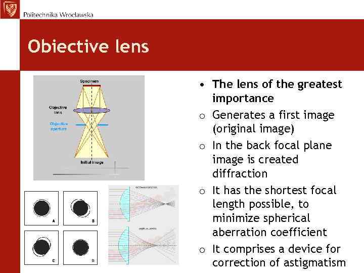 Obiective lens • The lens of the greatest importance o Generates a first image (original image) o In the back focal plane image is created diffraction o It has the shortest focal length possible, to minimize spherical aberration coefficient o It comprises a device for correction of astigmatism
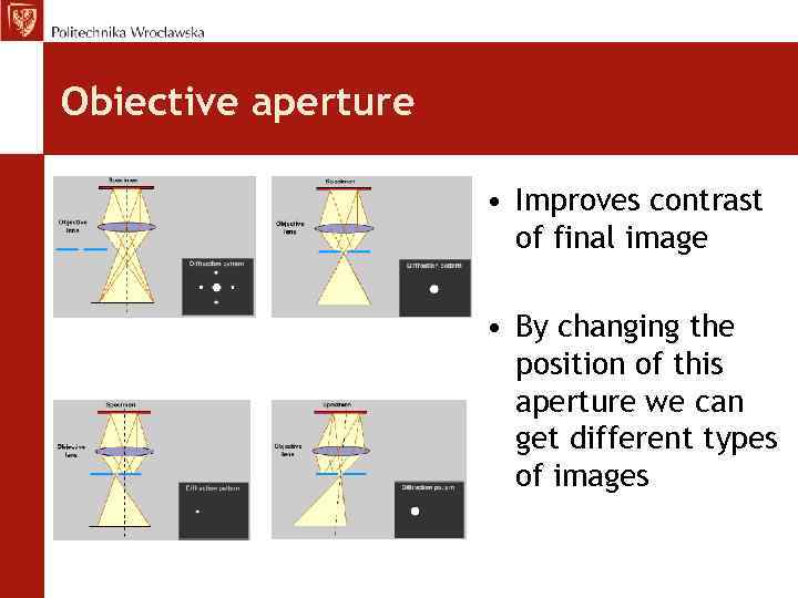 Obiective aperture • Improves contrast of final image • By changing the position of this aperture we can get different types of images
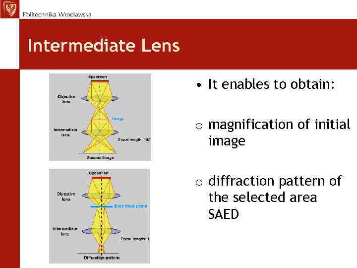 Intermediate Lens • It enables to obtain: o magnification of initial image o diffraction pattern of the selected area SAED
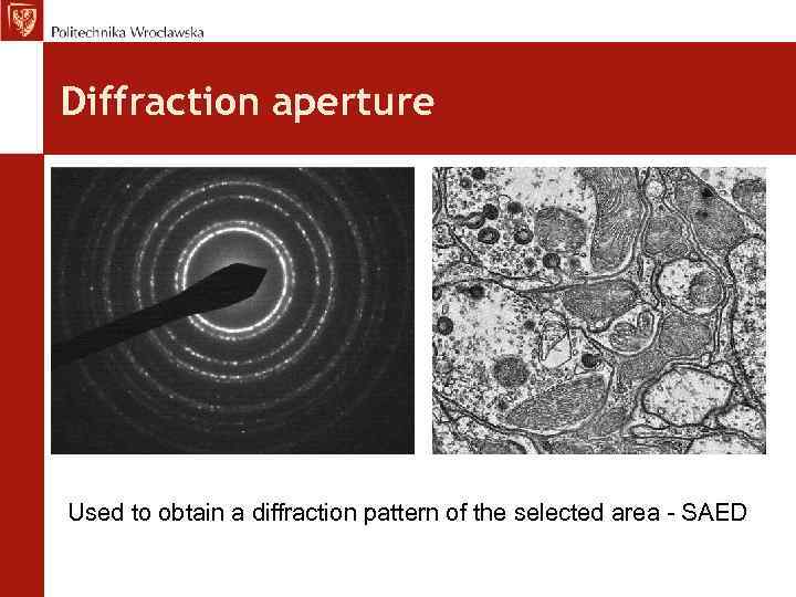 Diffraction aperture Used to obtain a diffraction pattern of the selected area - SAED
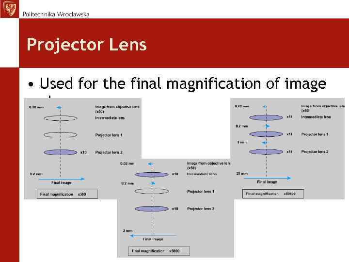 Projector Lens • Used for the final magnification of image obrazu
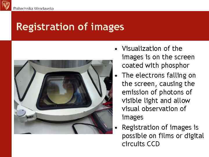 Registration of images • Visualization of the images is on the screen coated with phosphor • The electrons falling on the screen, causing the emission of photons of visible light and allow visual observation of images • Registration of images is possible on films or digital circuits CCD
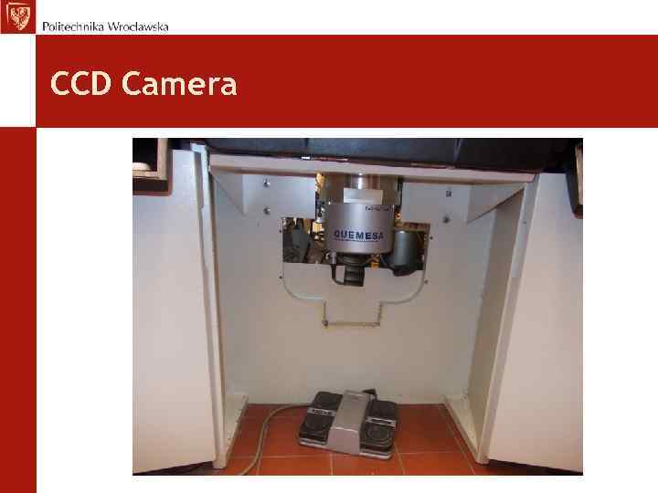 CCD Camera
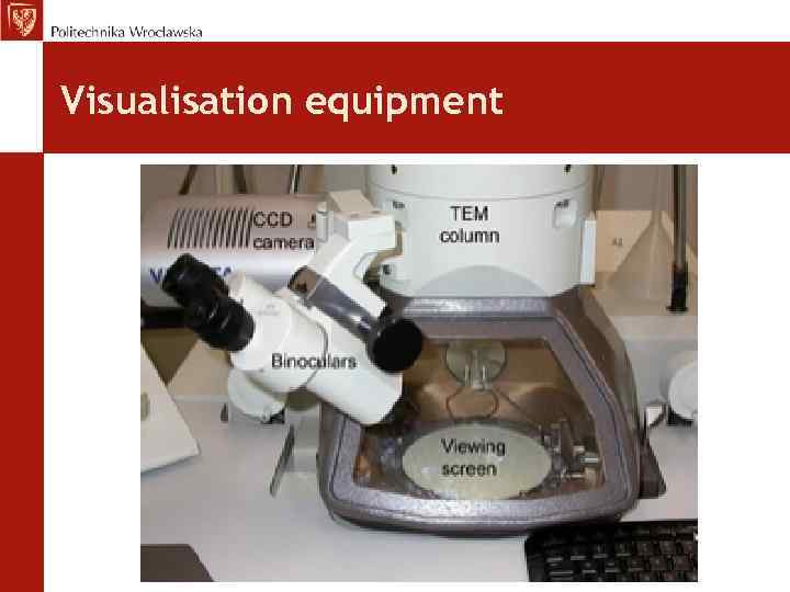 Visualisation equipment
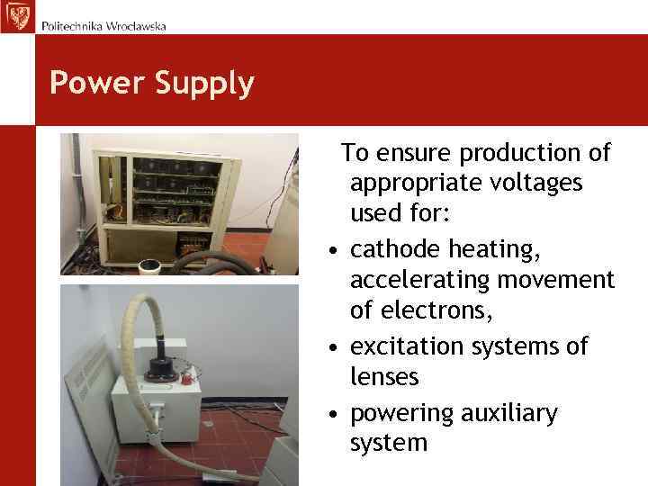 Power Supply To ensure production of appropriate voltages used for: • cathode heating, accelerating movement of electrons, • excitation systems of lenses • powering auxiliary system
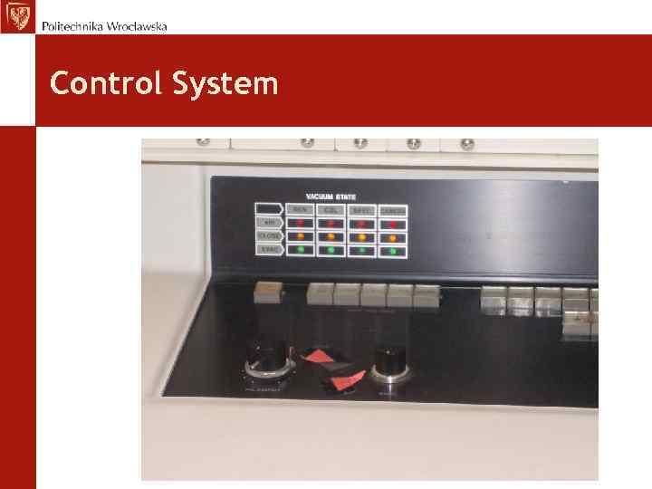 Control System
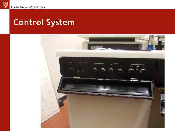 Control System
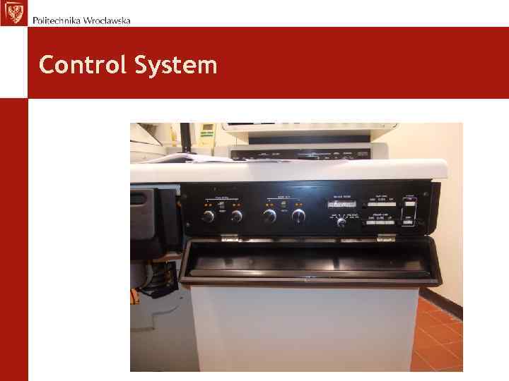 Control System
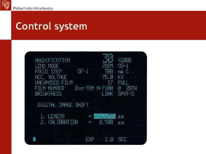 Control system
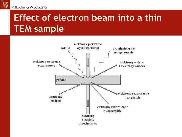 Effect of electron beam into a thin TEM sample
 Scanning Transmission Microscope STEM • Transmission electron microscope equipped with a transmission detector further analyzes the passing electrons. • In STEM may also include other detectors typical for SEM like: SE, BSE and X-ray • Advantages: o opportunity to observe specimens thicker than in the TEM o possibility to perform microanalysis by EDS or EELS
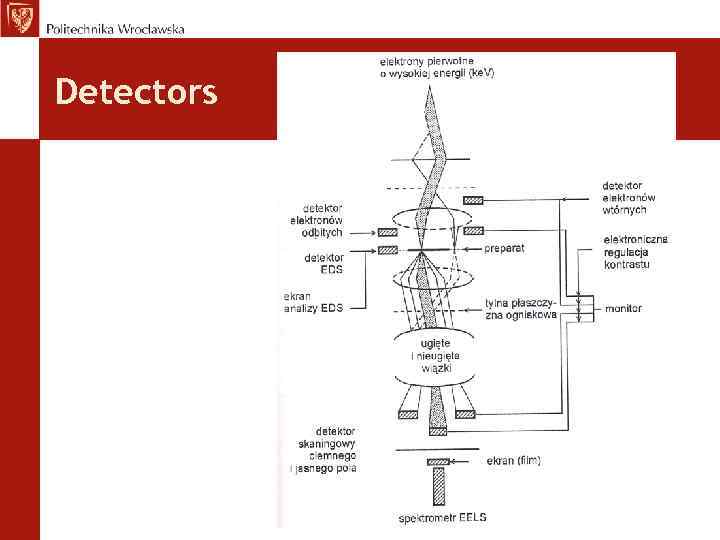 Detectors
 HVTEM / HRTEM • HVTEM – High Voltage TEM HRTEM – High Resolution TEM • • Used for studies crystalline samples It enables observation of atoms and atomic planes Zoom up to several million times It enables observation of crystal structure, crystal defects, the interphase boundaries. • It enables testing of thicker samples
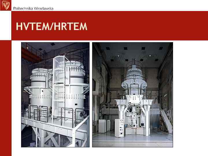 HVTEM/HRTEM
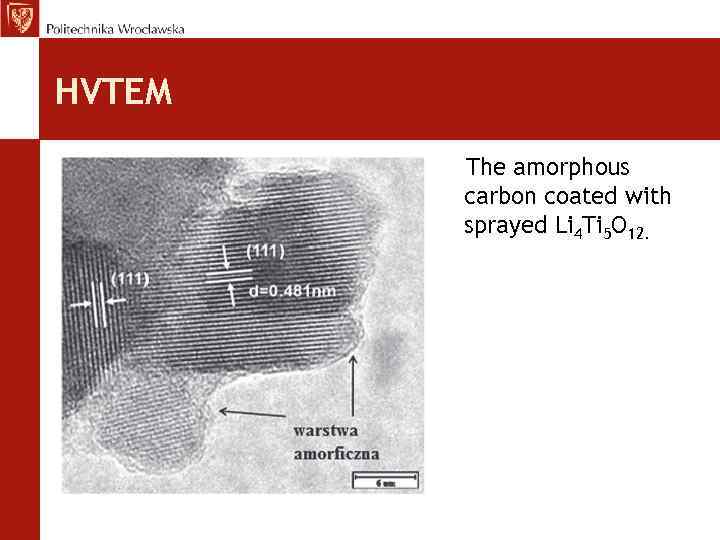 HVTEM The amorphous carbon coated with sprayed Li 4 Ti 5 O 12.
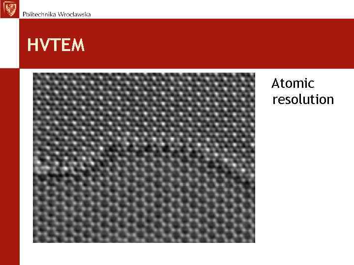 HVTEM Atomic resolution
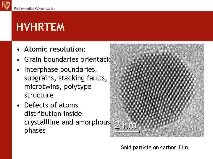 HVHRTEM • Atomic resolution: • Grain boundaries orientation • Interphase boundaries, subgrains, stacking faults, t microtwins, polytype structure • Defects of atoms distribution inside crystallline and amorphous phases Gold particle on carbon film
 EDS – X-ray radiation • X-ray - formed in the electron beam column takes an electron from an inner shell of the atom in the test sample. His place is taken by an electron from a higher energy shell emitting quantum characteristic energy • The radiation energy is characteristic of the element • Possible chemical composition - microanalysis (detection of elements)
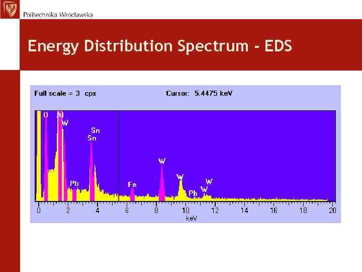 Energy Distribution Spectrum - EDS
 EELS – Electron Energy Loss Spectroscopy • Spectroscopy (EELS) - is based on the analysis of the energy distribution of scattered electrons. With such a collision the electron loses some part of their kinetic energy - the energy of the primary electrons E 0 is reduced by the value characteristic for the material • It is possible microanalysis chemical composition. • The EELS spectrometer is placed under the screen
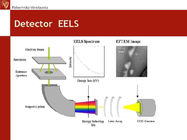 Detector EELS
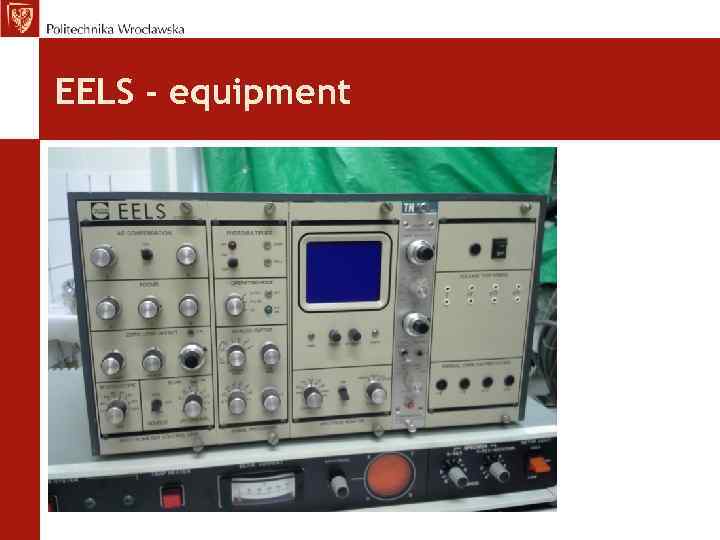 EELS - equipment
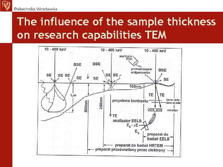 The influence of the sample thickness on research capabilities TEM
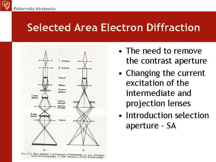 Selected Area Electron Diffraction • The need to remove the contrast aperture • Changing the current excitation of the intermediate and projection lenses • Introduction selection aperture - SA
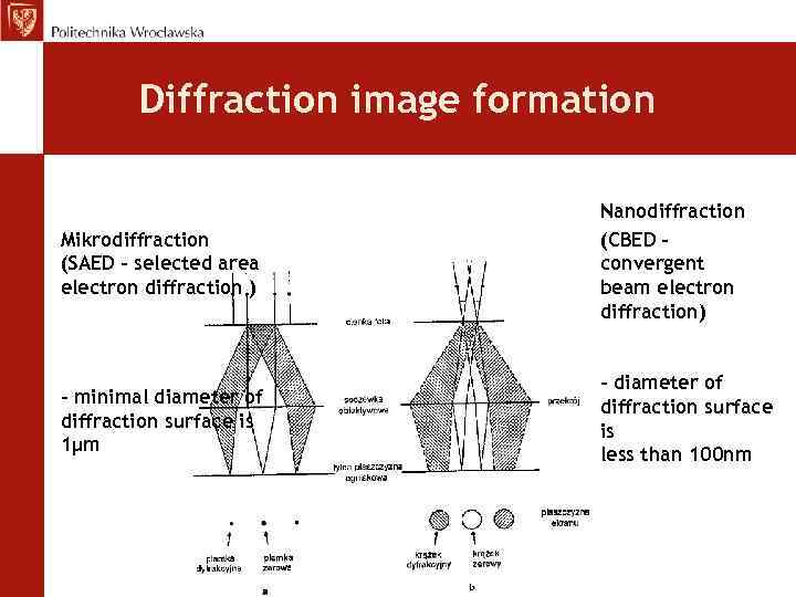 Diffraction image formation Mikrodiffraction (SAED – selected area electron diffraction ) Nanodiffraction (CBED – convergent beam electron diffraction) – minimal diameter of diffraction surface is 1μm – diameter of diffraction surface is less than 100 nm
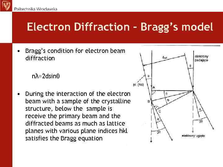 Electron Diffraction – Bragg’s model • Bragg’s condition for electron beam diffraction nλ=2 dsinθ • During the interaction of the electron beam with a sample of the crystalline structure, below the sample is receive the primary beam and the diffracted beams as much as lattice planes with various plane indices hkl satisfies the Bragg equation
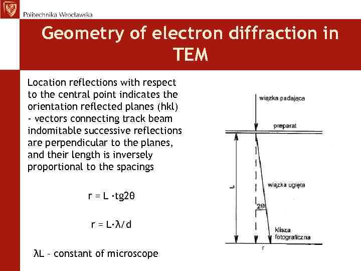 Geometry of electron diffraction in TEM Location reflections with respect to the central point indicates the orientation reflected planes (hkl) - vectors connecting track beam indomitable successive reflections are perpendicular to the planes, and their length is inversely proportional to the spacings r = L ·tg 2θ r = L·λ/d λL – constant of microscope
 Interpretation of electron diffraction patterns • Identification of the structure of the investigated crystal from which the reflections were formed • Indexing (specify indexes of atom planes) • Crystallographic analysis based on the diffraction image (SAED) • Applying the structure of the sample on the basis of the shape of elementary lattice and intensity of reflections
 Application of electron diffraction in materials investigation • Diffraction studies enable the identification of the observed phase • Identification of a polycrystal on the basis of the diffraction pattern is compared with the calculated measurement of the interplanar spacings with values contained in the databases of crystallographic data and determining the indices of {hkl} atom planes forming a diffraction pattern • In the case of a single crystal identification is a comprehensive solution diffraction pattern - defining indexes of atomic planes (hkl), zone axis [uvw] and their mutual crystallographic orientation
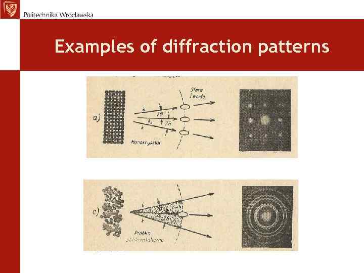 Examples of diffraction patterns
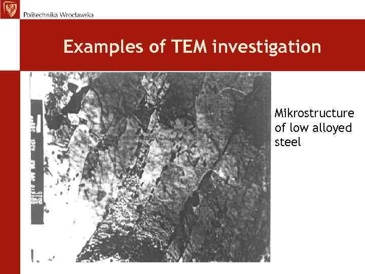 Examples of TEM investigation Mikrostructure of low alloyed steel
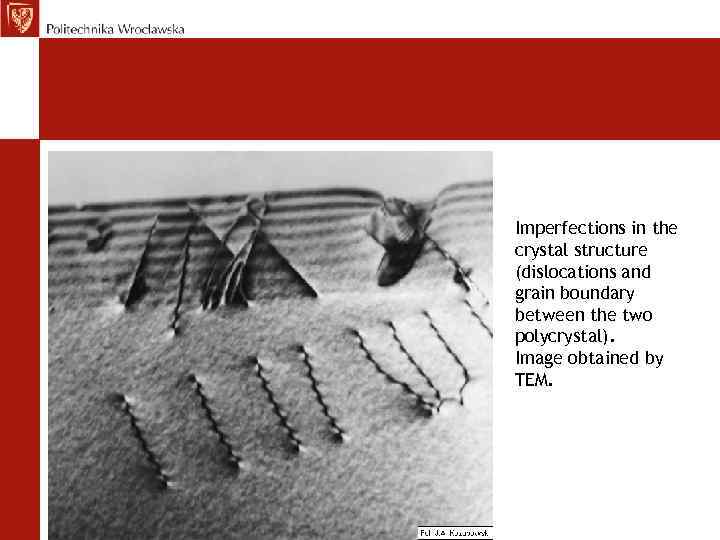 Imperfections in the crystal structure (dislocations and grain boundary between the two polycrystal). Image obtained by TEM.
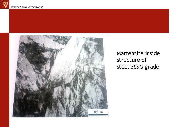 Martensite inside structure of steel 35 SG grade
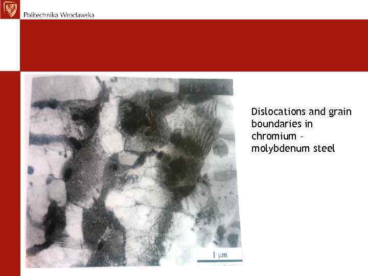 Dislocations and grain boundaries in chromium – molybdenum steel
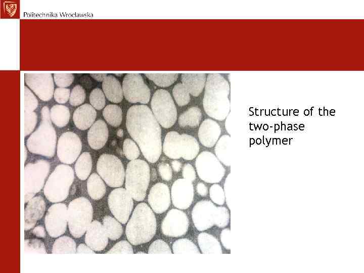 Structure of the two-phase polymer
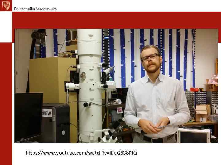 https: //www. youtube. com/watch? v=ii. Ju. G 636 Pf. Q
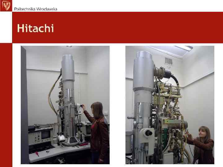 Hitachi
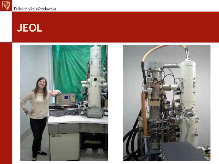 JEOL
JEOL
 Literatura • • G. Schimmel, Metodyka mikroskopii elektronowej, PWN, Warszawa 1976 Ian M. Wat, The principles and practice of electron microscopy, second edition, Cambridge University Press, 1997 Peter J. Goodhew, John Humphreys, Richard Beanland, Electron microscophy and analysis, third edition, Taylor & Francis Inc, London 2001 Andrzej Barbacki, Mikroskopia elektronowa, Wydawnictwo Politechniki Poznańskiej, Poznań 2005 Leszek A. Dobrzański, Eugeniusz Hajduczek, Mikroskopia świetlna i elektronowa, Wydawnictwa Naukowo-Techniczne, Warszawa 1987 Pod red. W. Dudzińskiego, Materiały konstrukcyjne w budowie maszyn, Oficyna Wydawnicza Politechniki Wrocławskiej, Wrocław 1994 Jan Kozubowski, Metody transmisyjnej mikroskopii elektronowej, Wydawnictwo Śląsk, Katowice 1975 Ludwig Reimer, Transmission Electron Microscopy, Spinger Verlag, Berlin. Heidelberg-New York-Tokyo 1984


