3fd2b42dba07663ecf8edb6f14ee5a24.ppt
- Количество слайдов: 17
 Technological challenges in particle detectors for future experiments 1. Glass Resistive Plate Chambers 2. IC based Silicon Detectors 3. Carbon Nanotube Integrated Silicon Pixel Detectors Det-04 B. Satyanarayana, TIFR, Mumbai Det-05 Anita Topkar & Bency John, BARC, Mumbai Det-14 Premomoy Ghosh & B. K. Nandi, VECC, Kolkata IGCAR, Kalpakkam, May 3 -4, 2004 Vision 2020 Subtopic 3. 8 Sensors, Detectors & NDT 1
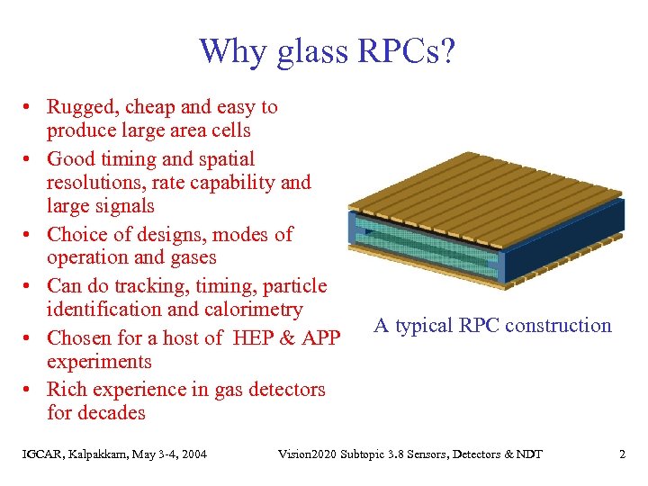 Why glass RPCs? • Rugged, cheap and easy to produce large area cells • Good timing and spatial resolutions, rate capability and large signals • Choice of designs, modes of operation and gases • Can do tracking, timing, particle identification and calorimetry • Chosen for a host of HEP & APP experiments • Rich experience in gas detectors for decades IGCAR, Kalpakkam, May 3 -4, 2004 A typical RPC construction Vision 2020 Subtopic 3. 8 Sensors, Detectors & NDT 2
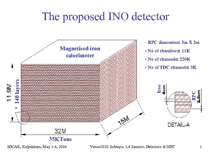 The proposed INO detector • RPC dimension: 3 m X 2 m Magnetised iron calorimeter • No of chambers: 11 K • No of channels: 220 K RPC Iron 140 layers • No of TDC channels: 3 K 35 KTons IGCAR, Kalpakkam, May 3 -4, 2004 Vision 2020 Subtopic 3. 8 Sensors, Detectors & NDT 3
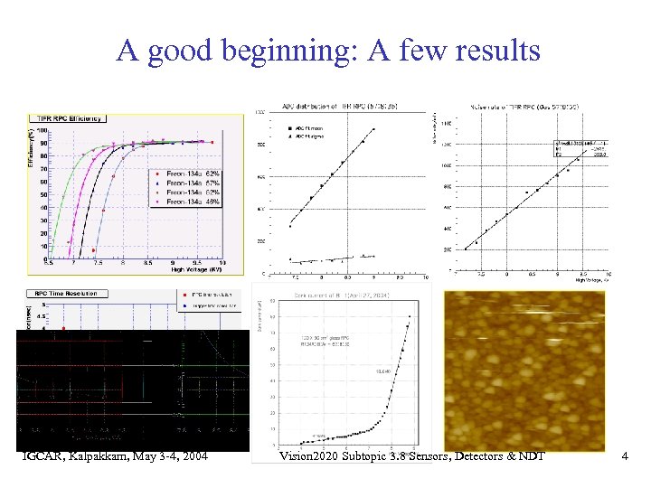 A good beginning: A few results IGCAR, Kalpakkam, May 3 -4, 2004 Vision 2020 Subtopic 3. 8 Sensors, Detectors & NDT 4
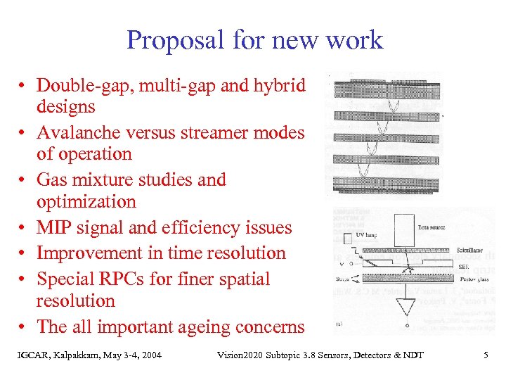 Proposal for new work • Double-gap, multi-gap and hybrid designs • Avalanche versus streamer modes of operation • Gas mixture studies and optimization • MIP signal and efficiency issues • Improvement in time resolution • Special RPCs for finer spatial resolution • The all important ageing concerns IGCAR, Kalpakkam, May 3 -4, 2004 Vision 2020 Subtopic 3. 8 Sensors, Detectors & NDT 5
 Proposed plan for new work • • Gases, mixing, circulation and monitoring systems Industrial help for resistive coats on electrodes etc. In-house development of electronics and DAQ Simulation studies – Process, Device and Detector Meeting INO design requirements in the process RPC deployments beyond INO Possible spinoffs … IGCAR, Kalpakkam, May 3 -4, 2004 Vision 2020 Subtopic 3. 8 Sensors, Detectors & NDT 6
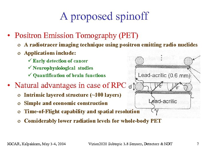 A proposed spinoff • Positron Emission Tomography (PET) o A radiotracer imaging technique using positron emitting radio nuclides o Applications include: ü Early detection of cancer ü Neurophysiological studies ü Quantification of brain functions • Natural advantages in case of RPC o Intrinsic layered structure (~100 layers) o Simple and economic construction o Time-of-Flight capability and spatial resolution o Considerably lower radiation levels for whole-body PET IGCAR, Kalpakkam, May 3 -4, 2004 Vision 2020 Subtopic 3. 8 Sensors, Detectors & NDT 7
 Silicon detectors: Past & Future • Developed silicon strip detectors for CMS experiment at CERN • Developed silicon PIN diodes of various sizes as a spin off • Recently, double sided processing has been established at our foundries • Requirements for future experiments o High resolution spectroscopy of charged particles o Particle identification o Low activity counting • Challenges for Silicon detector development o Double sided, ac coupled, micro strip detectors, pixel detectors o Detectors with large/small area, low leakage & minimum dead layer thickness o Detectors with uniform, controllable & thin active region IGCAR, Kalpakkam, May 3 -4, 2004 Vision 2020 Subtopic 3. 8 Sensors, Detectors & NDT 8
 Silicon detectors for future experiments • BARC Charged Particle Array for Nuclear Reaction Studies o 108 detector modules to be configured as a spherical array o Si-strip detectors to measure scattering angle and energy of charged particles o Cs. I(Tl)-PIN diode detectors to measure residual energy of light charged particles which penetrate Si-strip detectors • Participation in a Silicon Tracking System o Tracking charged particles directly with a compact Si-detector system o Vertex determination with a resolution better than 50 mm o Bulk area of the tracking stations to be covered with double sided Si-micro strip detectors o Compressed Baryonic Matter experiment at GSI, Darmstad, Germany has shown interest in our participation IGCAR, Kalpakkam, May 3 -4, 2004 Vision 2020 Subtopic 3. 8 Sensors, Detectors & NDT 9
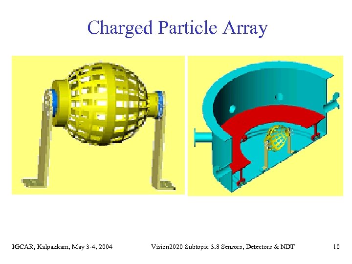 Charged Particle Array IGCAR, Kalpakkam, May 3 -4, 2004 Vision 2020 Subtopic 3. 8 Sensors, Detectors & NDT 10
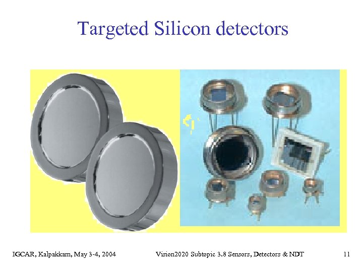 Targeted Silicon detectors IGCAR, Kalpakkam, May 3 -4, 2004 Vision 2020 Subtopic 3. 8 Sensors, Detectors & NDT 11
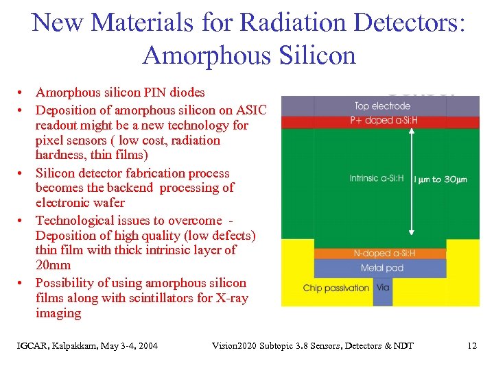 New Materials for Radiation Detectors: Amorphous Silicon • Amorphous silicon PIN diodes • Deposition of amorphous silicon on ASIC readout might be a new technology for pixel sensors ( low cost, radiation hardness, thin films) • Silicon detector fabrication process becomes the backend processing of electronic wafer • Technological issues to overcome Deposition of high quality (low defects) thin film with thick intrinsic layer of 20 mm • Possibility of using amorphous silicon films along with scintillators for X-ray imaging IGCAR, Kalpakkam, May 3 -4, 2004 Vision 2020 Subtopic 3. 8 Sensors, Detectors & NDT 12
 Carbon Nanotube Integrated Silicon Pixel Detectors The obvious choice for near vertex particle tracking is the Silicon Pixel detectors due to their compactness, good spatial resolution and low material budget Better spatial resolution is a constraint due to o Thickness of the sensor (Si-substrate) o Dimensions of Pixels o Dimensions of read-out chips Use of CNT helps in improving the last two of the above Concept of CNTISPD CNT junction diodes integrated with CNTFET-transistor (for first low-noise amplification) and CNT-conducting cables (for carrying charges to the read-out) can be grown on Si-wafer (substrate). The volume of read-out electronics can be further reduced with the help of nanoelectronics IGCAR, Kalpakkam, May 3 -4, 2004 Vision 2020 Subtopic 3. 8 Sensors, Detectors & NDT 13
 Feasibility of developing CNTISPD • Semiconducting CNTs provide higher electron-mobility than that of any known material at room temperature • Nano junction diodes and transistors are already in the scene. p-n junction diode has been developed at CNT-metal contact • Nanotubular ropes composed of aligned multiwalled nanotubes having electrically insulating outer shells and semiconducting inner shells have been synthesized • Vertically aligned CNTs have been deposited at predetermined position on pre-etched Silicon wafers • Stronger C-C bonding may be favourable in respect of radiation tolerance IGCAR, Kalpakkam, May 3 -4, 2004 Vision 2020 Subtopic 3. 8 Sensors, Detectors & NDT 14
 Challenges foreseen – needs R&D • Smaller implant-width provides larger gap-width and hence reduces the noise. We need to optimize this for a better charge collection • Besides the dimension of pixels, the other important R&D area for the pixel detectors is the thickness (presently ~. 25 mm) of the sensor (Si-wafer). Sensorthickness limits track resolution • And finally, the obvious challenges related to CNT technology IGCAR, Kalpakkam, May 3 -4, 2004 Vision 2020 Subtopic 3. 8 Sensors, Detectors & NDT 15
 Road map for the success of CNTISPD • Realization of this multidisciplinary endeavor requires parallel efforts to overcome the challenges involved in: o Indigenous development of present generation Pixel Detectors o Synthesis and assembly of patterned array of aligned CNTs o Development of CNT-based functional devices • Nanotechnology is already a thrust area in the DAE-program • Emphasis on R & D of CNT-based technology is expected • Parallel initiative for indigenous development of the Pixel Detectors of present generation is sought for • Finally, merging of the above three would make CNTISPD a reality IGCAR, Kalpakkam, May 3 -4, 2004 Vision 2020 Subtopic 3. 8 Sensors, Detectors & NDT 16
 Conclusions • We have already successfully developed and deployed some these detectors • Immediate applications in planned and future physics experiments are foreseen • Vision proposal for R & D in cutting-edge science and technology areas including: – New materials and/or hybrid designs – New processes and modes of operations – Simulation and optimization studies • Attractive spin-offs in diverse areas IGCAR, Kalpakkam, May 3 -4, 2004 Vision 2020 Subtopic 3. 8 Sensors, Detectors & NDT 17


