ac43ccb254435cf1369d02e3d2d69d75.ppt
- Количество слайдов: 24
System On Chip DAPNIA Day, November 10 th Presenter : Olivier REGNAULT / SILICA FAE Xilinx © 2006 Xilinx, Inc. All Rights Reserved
SOC Introduction • Challenge: – – – • Create High speed frequency design Use very High speed communication links Keep flexibility for modification Xilinx response: – – FPGA provides hardware structure that enables integrated high speed design (up to 550 Mhz) FPGA offers integrated differential solution (LVDS) for DDR high speed communication + Hard IP Transceiver (Up to 3. 2 Gbps) FPGA is by default the best hardware flexible solution offered through hardware reconfiguration (even partial reconfiguration) FPGA can implement processor core as • • Soft IP core (Microblaze) Hard IP core (Power. PC) System On Chip solution - 1 - 2 CEA Saclay, Dapnia day
Create High speed frequency design • • This is the first thing we expect from an FPGA. What we know : – – – FPGA can reproduce Chip set such as DSP FPGA enables parallel structure FPGA integrates features to improve performance and decrease the logic needs System On Chip solution - 1 - 3 CEA Saclay, Dapnia day
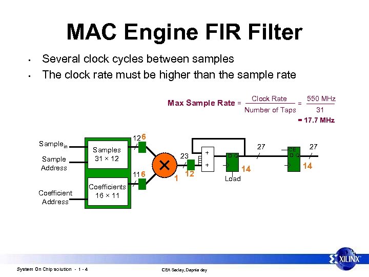
MAC Engine FIR Filter • • Several clock cycles between samples The clock rate must be higher than the sample rate Max Sample Rate = Samplein Sample Address Coefficient Address System On Chip solution - 1 - 4 Clock Rate Number of Taps = 550 MHz 31 = 17. 7 MHz 12 6 Samples 31 × 12 11 6 × 23 1 12 + 27 D Q + Coefficients 16 × 11 CEA Saclay, Dapnia day 14 Load CE D Q 27 14
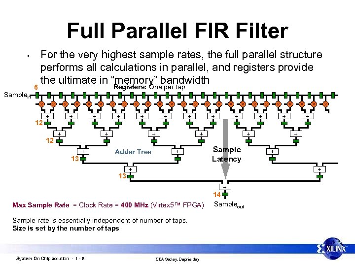
Full Parallel FIR Filter • Samplein 6 For the very highest sample rates, the full parallel structure performs all calculations in parallel, and registers provide the ultimate in “memory” bandwidth Registers: One per tap 12 + + + + 13 + + Adder Tree 13 + + + Sample Latency + + + Max Sample Rate = Clock Rate = 400 MHz (Virtex 5™ FPGA) Sample rate is essentially independent of number of taps. Size is set by the number of taps System On Chip solution - 1 - 5 + CEA Saclay, Dapnia day + 14 Sampleout
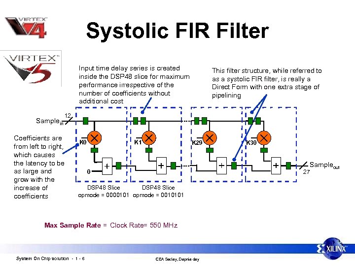
Systolic FIR Filter Input time delay series is created inside the DSP 48 slice for maximum performance irrespective of the number of coefficients without additional cost Samplein This filter structure, while referred to as a systolic FIR filter, is really a Direct Form with one extra stage of pipelining 12 Coefficients are from left to right, which causes the latency to be as large and grow with the increase of coefficients K 0 K 1 K 29 Sampleout 27 0 DSP 48 Slice opmode = 0000101 opmode = 0010101 Max Sample Rate = Clock Rate= 550 MHz System On Chip solution - 1 - 6 K 30 CEA Saclay, Dapnia day
Use very high Speed communication links • Components interconnection: – Data width may be large and may require a huge number of IOBs PCB Integrity signal Xilinx Sparse Chevron + LVDS • Power consumption LVDS • • System communication – Ethernet Xilinx includes Tri-mode MAC Hard IP (10/1000 Mbps) in Virtex 4 FX and Virtex 5 LXT – PCI Express Xilinx includes PCI Express Hard IP in the newest Virtex 5 LXT family. – PCIe x 1, x 2, x 4 and x 8 … System On Chip solution - 1 - 7 CEA Saclay, Dapnia day
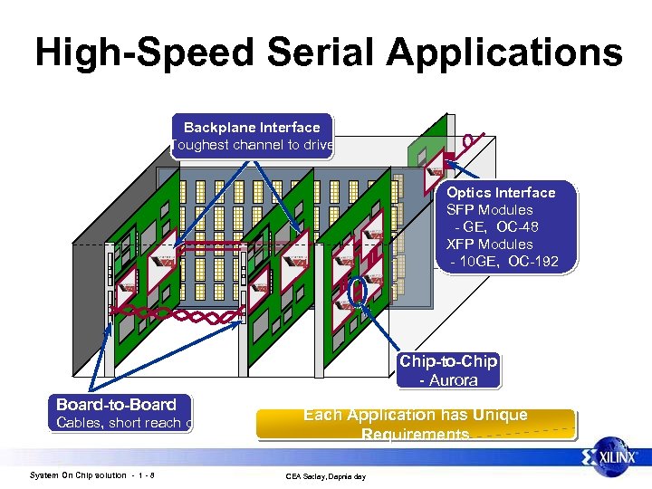
High-Speed Serial Applications Backplane Interface Toughest channel to drive Optics Interface SFP Modules - GE, OC-48 XFP Modules - 10 GE, OC-192 Chip-to-Chip - Aurora Board-to-Board Cables, short reach optics System On Chip solution - 1 - 8 Each Application has Unique Requirements CEA Saclay, Dapnia day
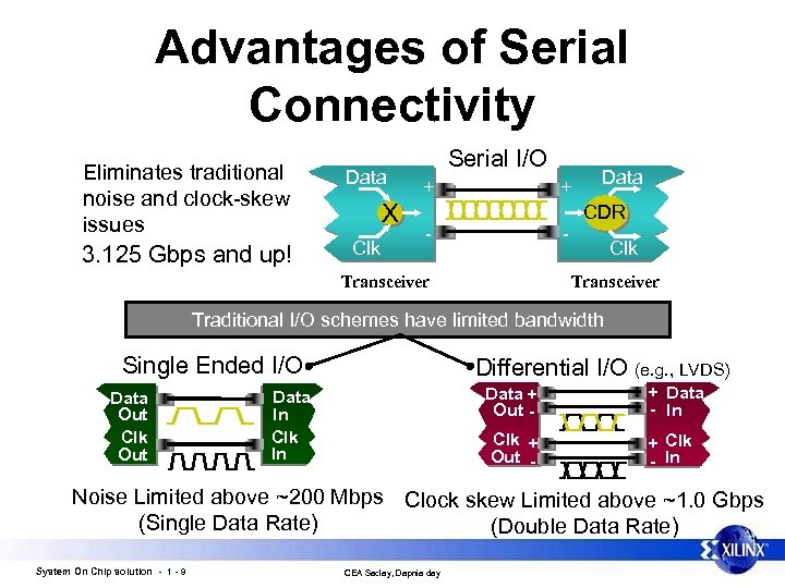
Advantages of Serial Connectivity Eliminates traditional noise and clock-skew issues 3. 125 Gbps and up! Data X Clk Serial I/O + + - - Transceiver Data CDR Clk Transceiver Traditional I/O schemes have limited bandwidth Single Ended I/O Data Out Clk Out Differential I/O (e. g. , LVDS) Data + Out - + Data - In Clk + Out - Data In Clk In + Clk - In Noise Limited above ~200 Mbps Clock skew Limited above ~1. 0 Gbps (Single Data Rate) (Double Data Rate) System On Chip solution - 1 - 9 CEA Saclay, Dapnia day
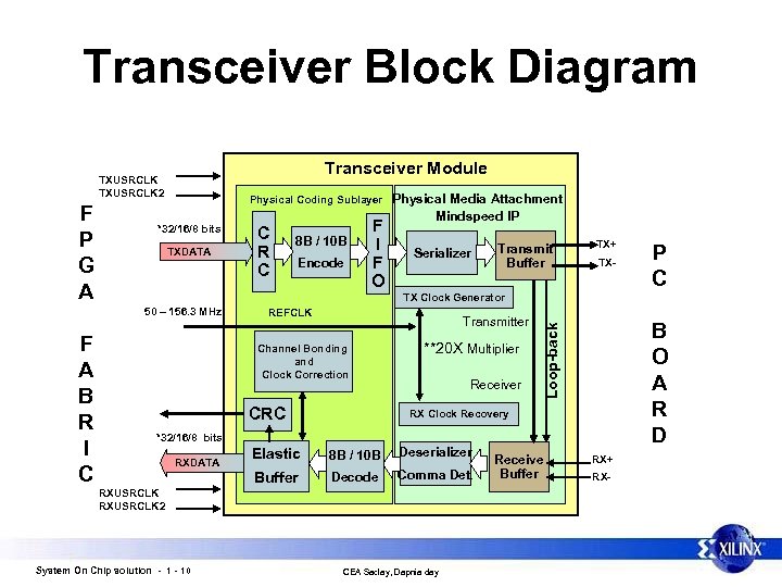
Transceiver Block Diagram F P G A Physical Coding Sublayer *32/16/8 bits C TXDATA R C 50 – 156. 3 MHz F A B R I C Transceiver Module 8 B / 10 B Encode F I F O Physical Media Attachment Mindspeed IP Serializer Transmit Buffer Transmitter CRC TX- **20 X Multiplier Receiver B O A R D RX Clock Recovery *32/16/8 bits Elastic 8 B / 10 B Deserializer Buffer RXDATA Decode Comma Det. RXUSRCLK 2 System On Chip solution - 10 P C TX Clock Generator REFCLK Channel Bonding and Clock Correction TX+ Loop-back TXUSRCLK 2 CEA Saclay, Dapnia day Receive Buffer RX+ RX-
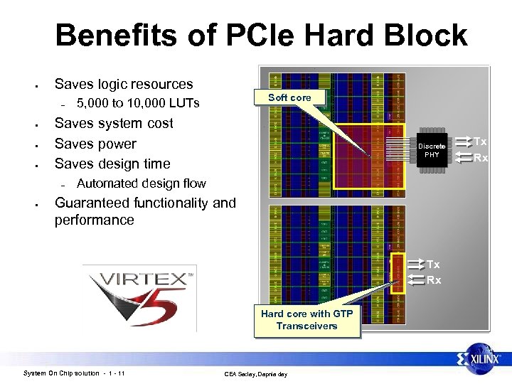
Benefits of PCIe Hard Block • Saves logic resources – • • • Saves system cost Saves power Saves design time – • Soft core 5, 000 to 10, 000 LUTs Discrete PHY Automated design flow Guaranteed functionality and performance Tx Rx Hard core with GTP Transceivers System On Chip solution - 11 CEA Saclay, Dapnia day Tx Rx
Keep Flexibility: Processor embedded in an FPGA • Processor embedded in an FPGA consists of the following – – FPGA hardware design Software design • • • Software routines Interrupt service routines (optional) Real Time Operating System (RTOS) (optional) System On Chip solution - 12 CEA Saclay, Dapnia day
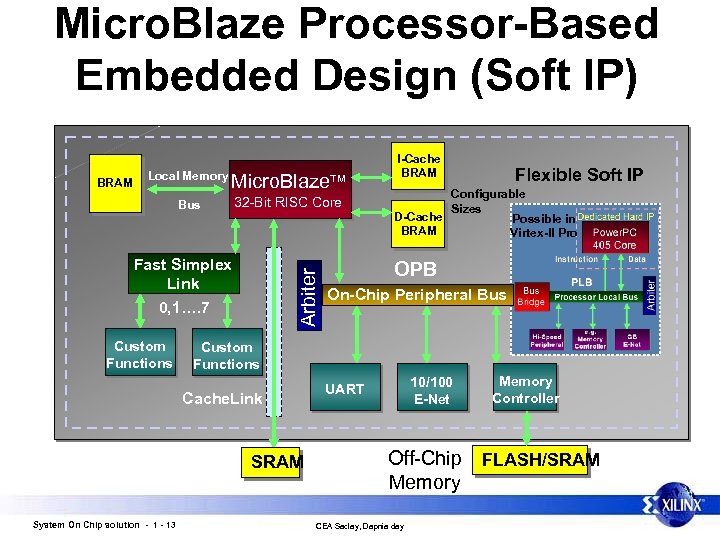
Micro. Blaze Processor-Based Embedded Design (Soft IP) BRAM Local Memory Micro. Blaze Bus 32 -Bit RISC Core Custom Functions Arbiter Fast Simplex Link 0, 1…. 7 Flexible Soft IP Configurable Sizes D-Cache Possible in BRAM Virtex-II Pro OPB On-Chip Peripheral Bus Custom Functions Cache. Link SRAM System On Chip solution - 13 I-Cache BRAM 10/100 E-Net UART Memory Controller Off-Chip FLASH/SRAM Memory CEA Saclay, Dapnia day
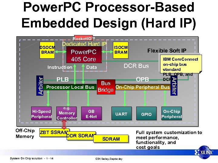
Power. PC Processor-Based Embedded Design (Hard IP) Rocket. IO™ DSOCM BRAM Dedicated Hard IP Power. PC 405 Core DCR Bus Data OPB PLB IBM Core. Connect on-chip bus standard PLB, OPB, and DCR Bus Processor Local Bus On-Chip Peripheral Bus Bridge Hi-Speed Peripheral Off-Chip Memory Flexible Soft IP e. g. Memory Controller GB E-Net ZBT SSRAM DDR SDRAM System On Chip solution - 14 UART SDRAM CEA Saclay, Dapnia day GPIO Arbiter Instruction ISOCM BRAM On-Chip Peripheral Full system customization to meet performance, functionality, and cost goals
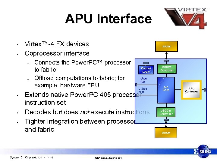
APU Interface • • Virtex™-4 FX devices Coprocessor interface – – • • • BRAM Connects the Power. PC™ processor to fabric Offload computations to fabric; for example, hardware FPU Control Logic I-Side PLB D-Side PLB Extends native Power. PC 405 processor instruction set Decodes but does not execute instructions Tighter integration between processor and fabric System On Chip solution - 15 CEA Saclay, Dapnia day ISOCM Controller 405 Core DSOCM Controller BRAM APU Controller
Embedded Development Kit • What is the Embedded Development Kit (EDK)? – – – The Embedded Development Kit is the Xilinx software suite for designing complete embedded programmable systems The kit includes all the tools, documentation, and IP that you require for designing systems with embedded IBM Power. PC™ hard processor cores, and/or Xilinx Micro. Blaze™ soft processor cores It enables the integration of both hardware and software components of an embedded system System On Chip solution - 16 CEA Saclay, Dapnia day
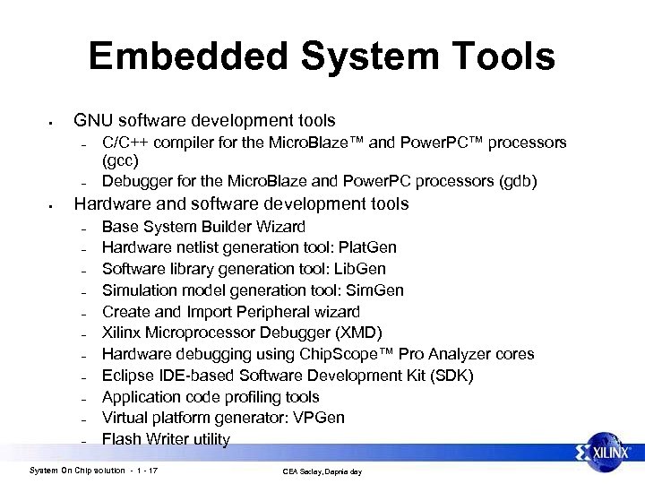
Embedded System Tools • GNU software development tools – – • C/C++ compiler for the Micro. Blaze™ and Power. PC™ processors (gcc) Debugger for the Micro. Blaze and Power. PC processors (gdb) Hardware and software development tools – – – Base System Builder Wizard Hardware netlist generation tool: Plat. Gen Software library generation tool: Lib. Gen Simulation model generation tool: Sim. Gen Create and Import Peripheral wizard Xilinx Microprocessor Debugger (XMD) Hardware debugging using Chip. Scope™ Pro Analyzer cores Eclipse IDE-based Software Development Kit (SDK) Application code profiling tools Virtual platform generator: VPGen Flash Writer utility System On Chip solution - 17 CEA Saclay, Dapnia day
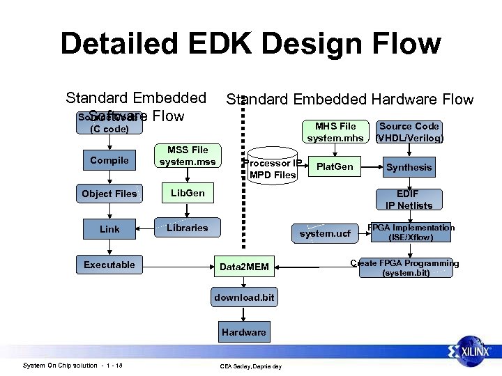
Detailed EDK Design Flow Standard Embedded Source Code Software Flow Standard Embedded Hardware Flow MHS File system. mhs (C code) Compile MSS File system. mss Object Files Libraries Plat. Gen Synthesis Lib. Gen Link Source Code (VHDL/Verilog) Executable Processor IP MPD Files EDIF IP Netlists system. ucf Data 2 MEM download. bit Hardware System On Chip solution - 18 CEA Saclay, Dapnia day FPGA Implementation (ISE/Xflow) Create FPGA Programming (system. bit)
Xilinx Solutions System On Chip solution - 19 CEA Saclay, Dapnia day
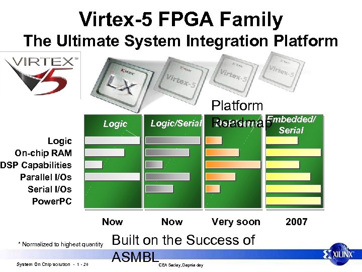
Virtex-5 FPGA Family The Ultimate System Integration Platform Logic/Serial Platform DSP/Serial Embedded/ Roadmap Serial Logic On-chip RAM DSP Capabilities Parallel I/Os Serial I/Os Power. PC Now * Normalized to highest quantity System On Chip solution - 1 - 20 Now Very soon Built on the Success of ASMBL CEA Saclay, Dapnia day 2007
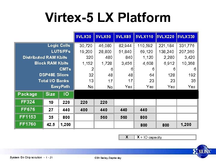
Virtex-5 LX Platform 5 VLX 30 Logic Cells LUT 6/FFs Distributed RAM Kbits Block RAM Kbits CMTs DSP 48 E Slices Total I/O Banks Easy. Path 30, 720 19, 200 320 1, 152 2 32 13 No 5 VLX 50 46, 080 28, 800 480 1, 728 6 48 17 No 5 VLX 85 82, 944 51, 840 3, 456 6 48 17 Yes 5 VLX 110 5 VLX 220 5 VLX 330 110, 592 69, 120 1, 120 4, 608 6 64 23 Yes Package Size IO FF 324 19 220 220 FF 676 27 440 400 440 440 FF 1153 35 800 560 800 FF 1760 42. 5 1, 200 221, 184 331, 776 138, 240 207, 360 2, 280 3, 420 6, 912 10, 368 6 6 128 192 23 35 Yes 800 X System On Chip solution - 1 - 21 CEA Saclay, Dapnia day X = IO capacity 800 1, 200
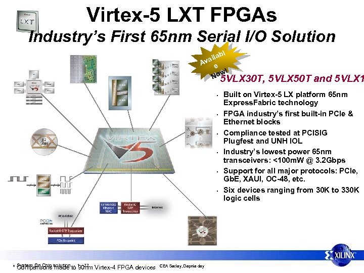
Virtex-5 LXT FPGAs Industry’s First 65 nm Serial I/O Solution bl aila Av e w! No 5 VLX 30 T, • • • System On Chip solution - 1 - 22 * Comparisons made to 90 nm Virtex-4 FPGA devices CEA Saclay, Dapnia day 5 VLX 50 T and 5 VLX 1 Built on Virtex-5 LX platform 65 nm Express. Fabric technology FPGA industry’s first built-in PCIe & Ethernet blocks Compliance tested at PCISIG Plugfest and UNH IOL Industry’s lowest power 65 nm transceivers: <100 m. W @ 3. 2 Gbps Support for all major protocols: PCIe, Gb. E, XAUI, OC-48, etc. Six devices ranging from 30 K to 330 K logic cells
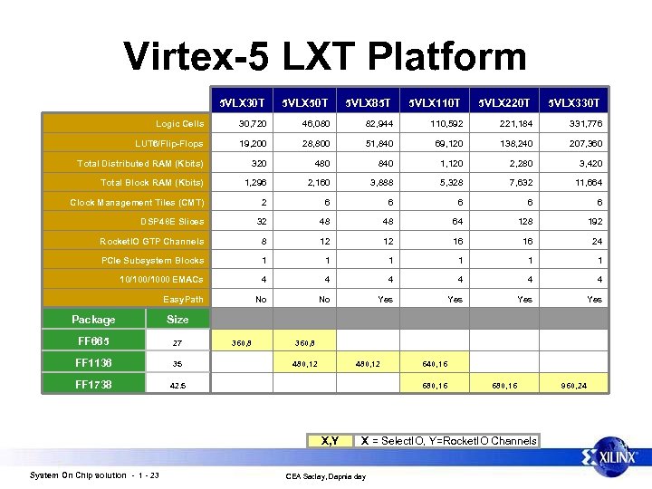
Virtex-5 LXT Platform 5 VLX 30 T 5 VLX 50 T 5 VLX 85 T 5 VLX 110 T 5 VLX 220 T 5 VLX 330 T Logic Cells 30, 720 46, 080 82, 944 110, 592 221, 184 331, 776 LUT 6/Flip-Flops 19, 200 28, 800 51, 840 69, 120 138, 240 207, 360 Total Distributed RAM (Kbits) 320 480 840 1, 120 2, 280 3, 420 Total Block RAM (Kbits) 1, 296 2, 160 3, 888 5, 328 7, 632 11, 664 Clock Management Tiles (CMT) 2 6 6 6 DSP 48 E Slices 32 48 48 64 128 192 Rocket. IO GTP Channels 8 12 12 16 16 24 PCIe Subsystem Blocks 1 1 1 10/1000 EMACs 4 4 4 Easy. Path No No Yes Yes Package Size FF 665 27 360, 8 FF 1136 35 480, 12 FF 1738 42. 5 X, Y System On Chip solution - 1 - 23 640, 16 680, 16 X = Select. IO, Y=Rocket. IO Channels CEA Saclay, Dapnia day 960, 24
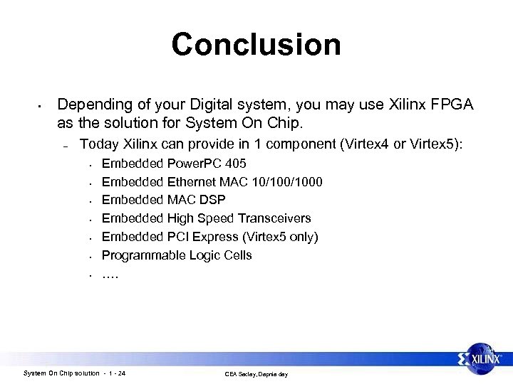
Conclusion • Depending of your Digital system, you may use Xilinx FPGA as the solution for System On Chip. – Today Xilinx can provide in 1 component (Virtex 4 or Virtex 5): • • Embedded Power. PC 405 Embedded Ethernet MAC 10/1000 Embedded MAC DSP Embedded High Speed Transceivers Embedded PCI Express (Virtex 5 only) Programmable Logic Cells …. System On Chip solution - 1 - 24 CEA Saclay, Dapnia day
ac43ccb254435cf1369d02e3d2d69d75.ppt