83c0ad9e050ce0746d4a46e463cfa6f8.ppt
- Количество слайдов: 16
SVT – Update Activities since Elba Meeting Super. B – Detector Meeting October, 9 2008 Giuliana Rizzo Universita’ & INFN Pisa G. Rizzo SVT- Update – October, 9 2008 1
Testbeam preparation • During the summer focus on the preparation of the September testbeam conclusion of the SLIM 5 3 years project. – Devices under test: first prototypes for SVT Layer 0 • CMOS MAPS matrix (4096 pixels, 50 x 50 um pitch) with on chip sparsified readout architecture. • Striplets modules (200 um thick) with FSSR 2 chips. – Many different parts built by the group to have a facility also for future tests on beam: • • Reference telescope with double sided strip detectors Prototype hybrids with FSSR 2 readout chips for strip/striplets Support table with xyz, theta motion New DAQ system for data push architecture (FSSR 2 and MAPS chips) • New Associative Memories board with LV 1 trigger capability G. Rizzo SVT- Update – October, 9 2008 2
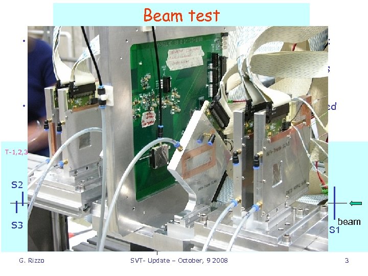
Beam test • Beam test 3 -16 September 2008 @ CERN (T 9). Main goals: – DNW MAPS matrix resolution & efficiency – Thin (200 mm) striplets module with FSSR 2 readout chips – Demostrate LVL 1 capability with tracker information sent to Associative Memories • Testbeam analysis ongoing: first encouraging results presented at the last Super. B Det Meeting by Nicola Neri. T-1, 2, 3, 4 : reference telescope modules Striplets-2 S 2 T-4, 3 MAPS-2 S 3 G. Rizzo T-2, 1 MAPS-1 Striplets-1 SVT- Update – October, 9 2008 beam S 1 3
SVT activities for TDR • Getting organized (funding!!!) for the TDR preparation. • In Italy: – Specific Super. B SVT R&D program for 2009 submitted to INFN. Funding request approved in September. • Institutions involved: Bologna, Milano, Pavia, Pisa, Roma III, Torino, Trieste ~ 18 FTE (~ 8 FTE are engineers) – With the same groups (+Perugia) 2 new R&D projects will start in 2009 ( 2011) to explore a very promising innovative microelectronic technology (Vertical Scale Integration) to realize ultra thin pixel detector system. The projects will be funded by the INFN and the Italian Ministry for Education and Research. • In UK: – Research program to participate to the TDR preparation will be submitted to the STFC for funding next week. – Activities proposed include R&D on the silicon strip detectors for the design and the optimization of external SVT layers. • Queen Mary and RAL Lab. involved G. Rizzo SVT- Update – October, 9 2008 4
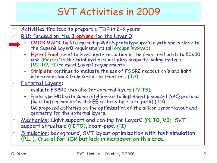
SVT Activities in 2009 • • • Activities finalized to prepare a TDR in 2 -3 years R&D focused on the 3 options for the Layer 0: – CMOS MAPS: build a multichip MAPS prototype module with specs close to the Super. B Layer 0 requirements (all groups involved) – Hybrid Pixel: need to investigate reduction in the front-end pitch to 50 x 50 um 2 (PV) and in the total material including support/cooling material (MI, TO, PI) to meet Layer 0 requirements. – Striplets: continue to evaluate the use of FSSR 2 readout chip and light interconnections from sensor to front-end (TS) External Layers: – evaluate FSSR 2 chip also for external layers (PV, TS), – Prototype HDI with some intelligence to implement proposed DAQ protocol (local buffer needed with FEE architecture data push) (TS) – UK proposed activities on the optimization of the silicon sensor layout and geometry for the external layers. Mechanics: Light support and cooling for Layer 0 (PI, TO, MI), SVT support structure (PI, TO), beam-pipe. (PI) Simulation: background, SVT layout optimization with fast simulation (PI…). Crucial for TDR but lack in manpower on this area. G. Rizzo SVT- Update – October, 9 2008 5
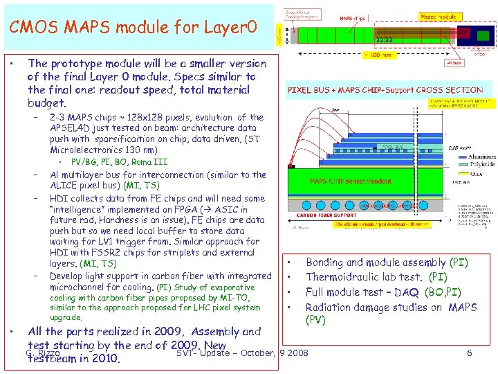
CMOS MAPS module for Layer 0 • The prototype module will be a smaller version of the final Layer 0 module. Specs similar to the final one: readout speed, total material budget. – – 2 -3 MAPS chips ~ 128 x 128 pixels, evolution of the APSEL 4 D just tested on beam: architecture data push with sparsificaition on chip, data driven, (ST Microlelectronics 130 nm) • PV/BG, PI, BO, Roma III Al multilayer bus for interconnection (similar to the ALICE pixel bus) (MI, TS) HDI collects data from FE chips and will need some “intelligence” implemented on FPGA ( ASIC in future rad. Hardness is an issue). FE chips are data push but so we need local buffer to store data waiting for LV 1 trigger from. Similar approach for HDI with FSSR 2 chips for striplets and external layers. (MI, TS) Develop light support in carbon fiber with integrated microchannel for cooling. (PI) Study of evaporative cooling with carbon fiber pipes proposed by MI-TO, similar to the approach proposed for LHC pixel system upgrade. • • • Bonding and module assembly (PI) Thermoidraulic lab test. (PI) Full module test – DAQ (BO, PI) Radiation damage studies on MAPS (PV) All the parts realized in 2009, Assembly and test starting by the end of 2009. New G. Rizzo SVT- Update – October, 9 2008 testbeam in 2010. 6
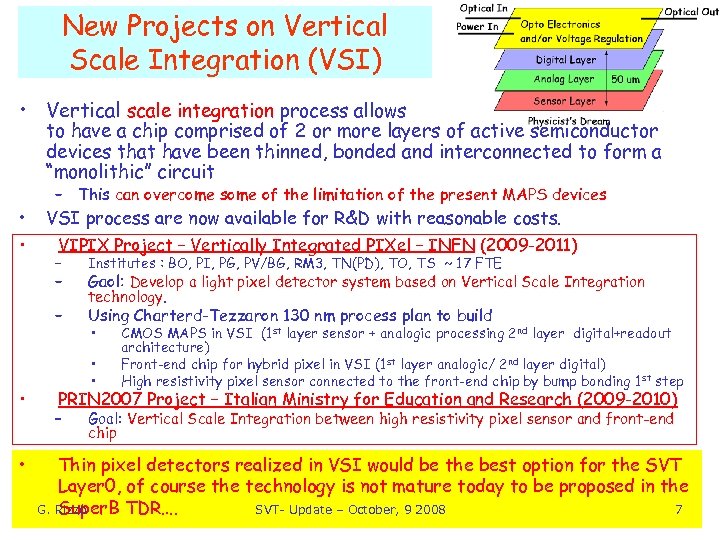
New Projects on Vertical Scale Integration (VSI) • Vertical scale integration process allows to have a chip comprised of 2 or more layers of active semiconductor devices that have been thinned, bonded and interconnected to form a “monolithic” circuit • • – This can overcome some of the limitation of the present MAPS devices VSI process are now available for R&D with reasonable costs. VIPIX Project – Vertically Integrated PIXel – INFN (2009 -2011) – – – • • Institutes : BO, PI, PG, PV/BG, RM 3, TN(PD), TO, TS ~ 17 FTE Gaol: Develop a light pixel detector system based on Vertical Scale Integration technology. Using Charterd-Tezzaron 130 nm process plan to build • • • CMOS MAPS in VSI (1 st layer sensor + analogic processing 2 nd layer digital+readout architecture) Front-end chip for hybrid pixel in VSI (1 st layer analogic/ 2 nd layer digital) High resistivity pixel sensor connected to the front-end chip by bump bonding 1 st step PRIN 2007 Project – Italian Ministry for Education and Research (2009 -2010) – Goal: Vertical Scale Integration between high resistivity pixel sensor and front-end chip Thin pixel detectors realized in VSI would be the best option for the SVT Layer 0, of course the technology is not mature today to be proposed in the G. Rizzo SVT- Update – October, 9 2008 7 Super. B TDR….

Backup G. Rizzo SVT- Update – October, 9 2008 8
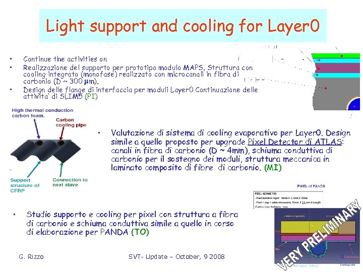
Light support and cooling for Layer 0 • • Continue the activities on Realizzazione del supporto per prototipo modulo MAPS. Struttura con cooling integrato (monofase) realizzato con microcanali in fibra di carbonio (D ~ 300 mm). Design delle flange di interfaccia per moduli Layer 0 Continuazione delle attivita’ di SLIM 5 (PI) • • • Valutazione di sistema di cooling evaporativo per Layer 0. Design simile a quello proposto per upgrade Pixel Detector di ATLAS: canali in fibra di carbonio (D ~ 4 mm), schiuma conduttiva di carbonio per il sostegno dei moduli, struttura meccanica in laminato composito di fibre di carbonio. (MI) Studio supporto e cooling per pixel con struttura a fibra di carbonio e schiuma conduttiva simile a quello in corso di elaborazione per PANDA (TO) G. Rizzo SVT- Update – October, 9 2008 9
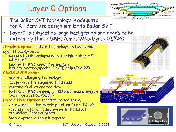
Layer 0 Options • The Ba. Bar SVT technology is adequate for R > 3 cm: use design similar to Ba. Bar SVT • Layer 0 is subject to large background and needs to be extremely thin: > 5 MHz/cm 2, 1 MRad/yr, < 0. 5%X 0 Striplets option: mature technology, not so robust against background. • Marginal with background rate higher than ~ 5 MHz/cm 2 • Moderate R&D needed on module interconnection/mechanics/FE chip (FSSR 2) CMOS MAPS option • new & challenging technology: • can provide the required thickness • existing devices are too slow • Extensive R&D ongoing (SLIM 5 -Collaboration) on 3 -well devices 50 x 50 um 2 Hybrid Pixel Option: tends to be too thick. • An example: Alice hybrid pixel module ~ 1% X 0 • Possible material reduction with the latest technology improvements • Viable option, although marginal G. Rizzo SVT- Update – October, 9 2008 10
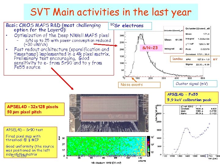
SVT Main activities in the last year 90 Sr electrons Basic CMOS MAPS R&D (most challenging option for the Layer 0): • Optimization of the Deep NWell MAPS pixel – • S/N up to 25 with power consumption reduced (~30 u. W/ch) S/N=23 Fast redout architecture (sparsification and timestamp) implemented in a 4 k pixel matrix. Preliminary test encouraging. Good sensitivity to e- from Sr 90 and to g from Fe 55 source Landau Noise events m. V Cluster signal (m. V) APSEL 4 D - Fe 55 5. 9 ke. V calibration peak APSEL 4 D - 32 x 128 pixels 50 mm pixel pitch APSEL 4 D – Sr 90 test Fired pixel map with threshodl @ ½ MIP Good uniformity (the source was positioned on the left side of the matrix G. Rizzo SVT- Update – October, 9 2008 11
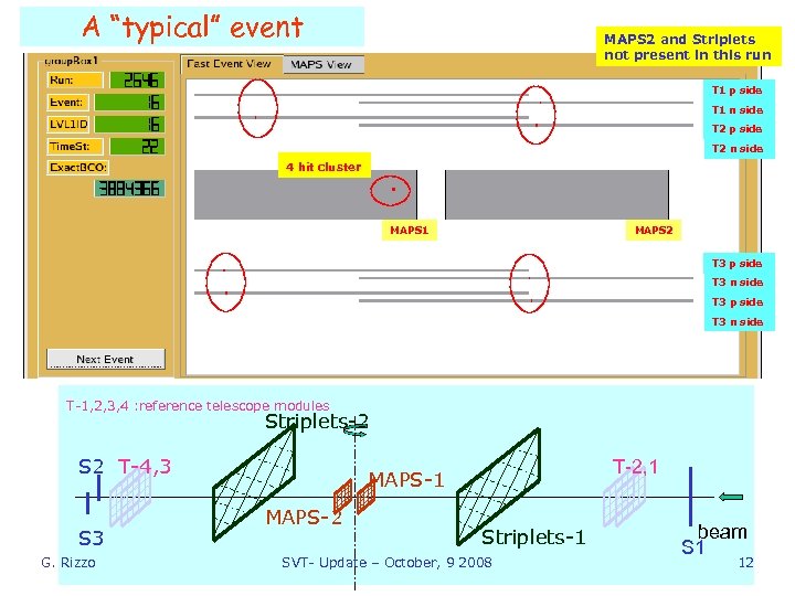
A “typical” event MAPS 2 and Striplets not present in this run T 1 p side T 1 n side T 2 p side T 2 n side 4 hit cluster MAPS 1 MAPS 2 T 3 p side T 3 n side T-1, 2, 3, 4 : reference telescope modules Striplets-2 S 2 T-4, 3 S 3 G. Rizzo T-2, 1 MAPS-2 Striplets-1 SVT- Update – October, 9 2008 beam S 1 12
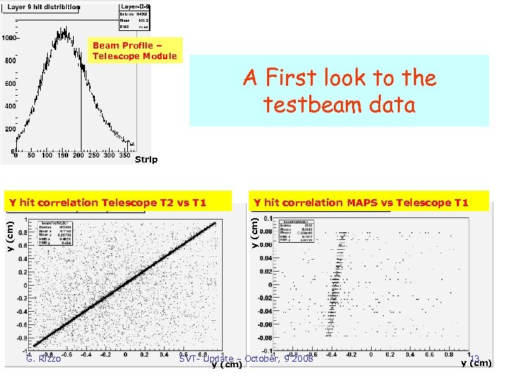
Beam Profile – Telescope Module A First look to the testbeam data Strip Y hit correlation MAPS vs Telescope T 1 y (cm) Y hit correlation Telescope T 2 vs T 1 G. Rizzo SVT- Update – October, 9 2008 y (cm) y 13 (cm)
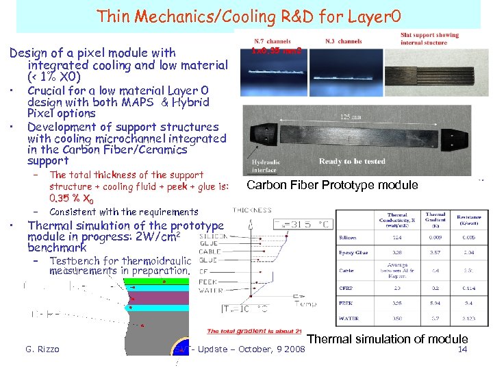
Thin Mechanics/Cooling R&D for Layer 0 Design of a pixel module with integrated cooling and low material (< 1% X 0) • Crucial for a low material Layer 0 • design with both MAPS & Hybrid Pixel options Development of support structures with cooling microchannel integrated in the Carbon Fiber/Ceramics support – • 1 x 0. 35 mm 2 – The total thickness of the support structure + cooling fluid + peek + glue is: 0. 35 % X 0 Consistent with the requirements Carbon Fiber Prototype module Thermal simulation of the prototype module in progress: 2 W/cm 2 benchmark – Testbench for thermoidraulic measurements in preparation. G. Rizzo SVT- Update – October, 9 2008 Thermal simulation of module 14
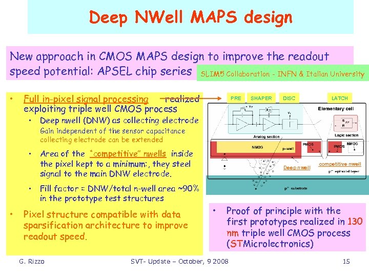
Deep NWell MAPS design New approach in CMOS MAPS design to improve the readout speed potential: APSEL chip series SLIM 5 Collaboration - INFN & Italian University • Full in-pixel signal processing realized exploiting triple well CMOS process PRE SHAPER DISC LATCH • Deep nwell (DNW) as collecting electrode Gain independent of the sensor capacitance collecting electrode can be extended • Area of the “competitive” nwells inside the pixel kept to a minimum: , they steel signal to the main DNW electrode. • Fill factor = DNW/total n-well area ~90% in the prototype test structures • Pixel structure compatible with data sparsification architecture to improve readout speed. G. Rizzo Deep nwell • competitive nwell Proof of principle with the first prototypes realized in 130 nm triple well CMOS process (STMicrolectronics) SVT- Update – October, 9 2008 15
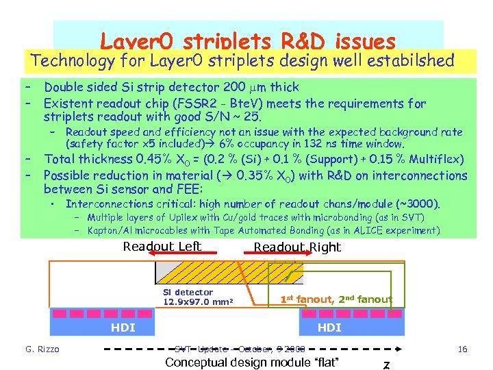
Layer 0 striplets R&D issues Technology for Layer 0 striplets design well estabilshed – – Double sided Si strip detector 200 mm thick Existent readout chip (FSSR 2 - Bte. V) meets the requirements for striplets readout with good S/N ~ 25. – Readout speed and efficiency not an issue with the expected background rate (safety factor x 5 included) 6% occupancy in 132 ns time window. Total thickness 0. 45% X 0 = (0. 2 % (Si) + 0. 1 % (Support) + 0. 15 % Multiflex) Possible reduction in material ( 0. 35% X 0) with R&D on interconnections between Si sensor and FEE: • Interconnections critical: high number of readout chans/module (~3000). – Multiple layers of Upilex with Cu/gold traces with microbonding (as in SVT) – Kapton/Al microcables with Tape Automated Bonding (as in ALICE experiment) Readout Left Si detector 12. 9 x 97. 0 mm 2 Readout Right 1 st fanout, 2 nd fanout HDI G. Rizzo HDI SVT- Update – October, 9 2008 Conceptual design module “flat” z 16
83c0ad9e050ce0746d4a46e463cfa6f8.ppt