55b3a3f6280d54870bb63829f7c9cce6.ppt
- Количество слайдов: 26
 Survey of Digital Signal Processors Michael Warner ECD: VLSI Communication Systems
 Agenda § Industry Trends § DSP Architecture § DSP Micro-Architecture § DSP Systems
 Agenda § Industry Trends § DSP Architecture § DSP Micro-Architecture § DSP Systems
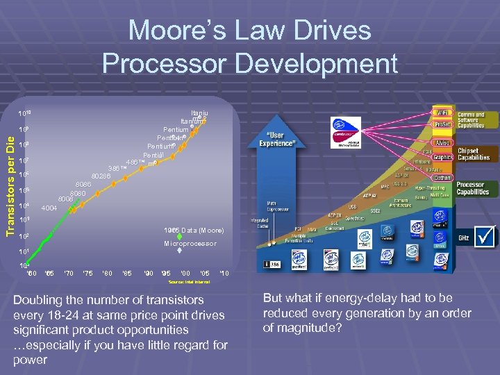 Moore’s Law Drives Processor Development Itaniu m® Itanium 2 ® Pentium ® 4 Pentium® III II Pentiu 486™ m® 386™ 80286 8080 8008 1010 Transistors per Die 109 108 107 106 105 104 4004 103 1965 Data (Moore) 102 Microprocessor 101 100 ‘ 65 ‘ 70 ‘ 75 ‘ 80 ‘ 85 ‘ 90 ‘ 95 ‘ 00 ‘ 05 ‘ 10 Source: Intel internal Doubling the number of transistors every 18 -24 at same price point drives significant product opportunities …especially if you have little regard for power But what if energy-delay had to be reduced every generation by an order of magnitude?
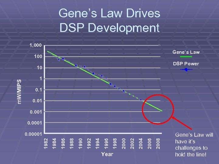 Gene’s Law Drives DSP Development 1, 000 Gene’s Law 100 DSP Power 1 0. 01 0. 0001 Year 2008 2006 2004 2002 2000 1998 1996 1994 1992 1990 1988 1986 1984 0. 00001 1982 m. W/MIPS 10 Gene’s Law will have it’s challenges to hold the line!
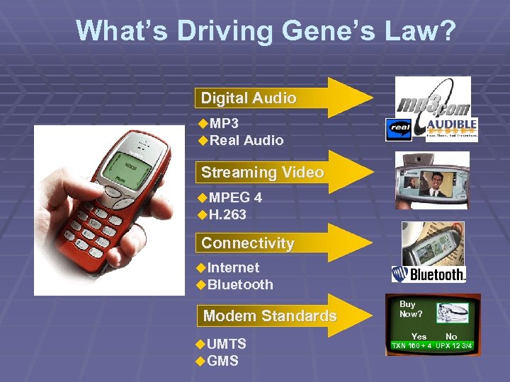 What’s Driving Gene’s Law? Digital Audio u MP 3 u Real Audio Streaming Video u MPEG 4 u H. 263 Connectivity u Internet u Bluetooth Modem Standards u UMTS u GMS Buy Now? Yes No TXN 160 + 4 UPX 12 3/4
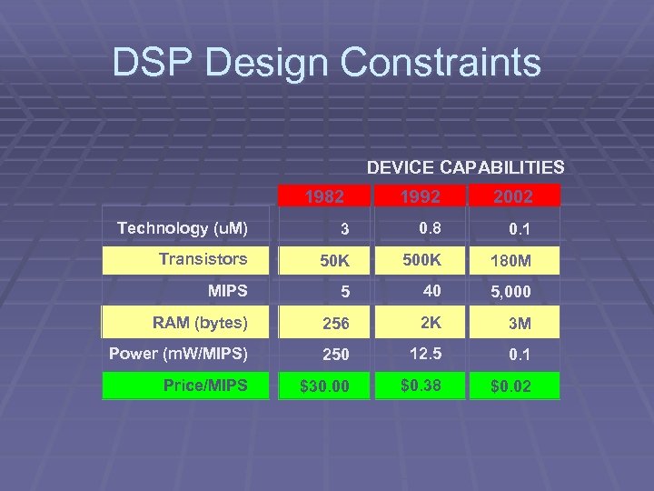 DSP Design Constraints DEVICE CAPABILITIES 1982 1992 2002 Technology (u. M) 3 0. 8 0. 1 Transistors 50 K 500 K 180 M MIPS 5 40 5, 000 RAM (bytes) 256 2 K 3 M Power (m. W/MIPS) 250 12. 5 0. 1 Price/MIPS $30. 00 $0. 38 $0. 02
 Agenda § Industry Trends § DSP Architecture § DSP Micro-Architecture § DSP Systems
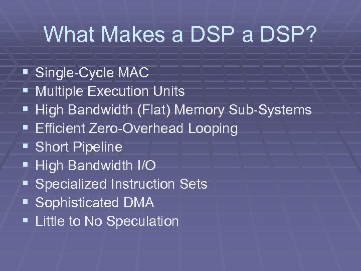 What Makes a DSP? § § § § § Single-Cycle MAC Multiple Execution Units High Bandwidth (Flat) Memory Sub-Systems Efficient Zero-Overhead Looping Short Pipeline High Bandwidth I/O Specialized Instruction Sets Sophisticated DMA Little to No Speculation
 Single Cycle MAC § MAC’s Typically Determine DSP Performance and Pipeline Length (EX) § Most DSP’s Have 2 -8 MAC Units § MAC’s Typically Operate in Both a Scalar and Vector Mode
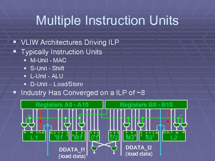 Multiple Instruction Units § VLIW Architectures Driving ILP § Typically Instruction Units § § M-Unit - MAC S-Unit - Shift L-Unit - ALU D-Unit – Load/Store § Industry Has Converged on a ILP of ~8 Registers A 0 - A 15 Registers B 0 - B 15 1 X S 1 2 X S 2 D DL SL L 1 SL D D S L 1 S 2 S D 1 S 2 M 1 DDATA_I 1 (load data) D S S 1 2 D 1 S S D 2 1 D 2 S 1 D M 2 S D D SL 1 L S 2 DDATA_I 2 (load data) SL DL D S 2 L 2 S 1
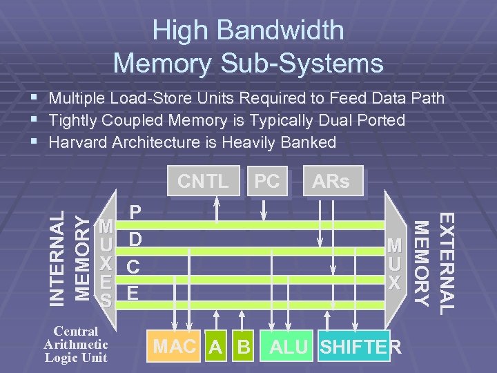 High Bandwidth Memory Sub-Systems § Multiple Load-Store Units Required to Feed Data Path § Tightly Coupled Memory is Typically Dual Ported § Harvard Architecture is Heavily Banked M U X E S Central Arithmetic Logic Unit P D C E PC ARs M U X MAC A B ALU SHIFTER EXTERNAL MEMORY INTERNAL MEMORY CNTL
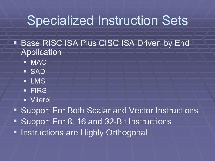 Specialized Instruction Sets § Base RISC ISA Plus CISC ISA Driven by End Application § § § § MAC SAD LMS FIRS Viterbi Support For Both Scalar and Vector Instructions Support For 8, 16 and 32 -Bit Instructions are Highly Orthogonal
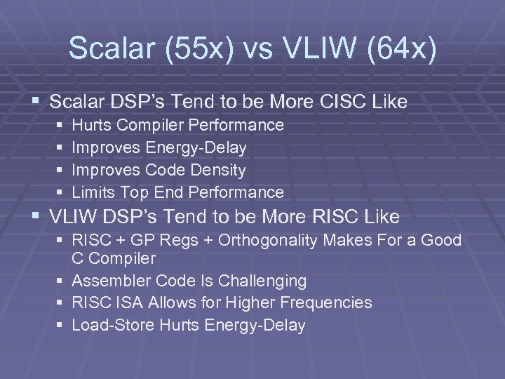 Scalar (55 x) vs VLIW (64 x) § Scalar DSP’s Tend to be More CISC Like § § Hurts Compiler Performance Improves Energy-Delay Improves Code Density Limits Top End Performance § VLIW DSP’s Tend to be More RISC Like § RISC + GP Regs + Orthogonality Makes For a Good C Compiler § Assembler Code Is Challenging § RISC ISA Allows for Higher Frequencies § Load-Store Hurts Energy-Delay
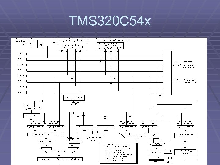 TMS 320 C 54 x
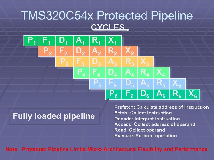 TMS 320 C 54 x Protected Pipeline CYCLES P 1 F 1 D 1 A 1 P 2 F 2 D 2 P 3 F 3 P 4 R 1 A 2 D 3 F 4 P 5 Fully loaded pipeline X 1 R 2 A 3 D 4 F 5 P 6 X 2 R 3 A 4 D 5 F 6 X 3 R 4 X 4 A 5 R 5 X 5 D 6 A 6 R 6 X 6 Prefetch: Calculate address of instruction Fetch: Collect instruction Decode: Interpret instruction Access: Collect address of operand Read: Collect operand Execute: Perform operation Note: Protected Pipeline Limits Micro-Architectural Flexibility and Performance
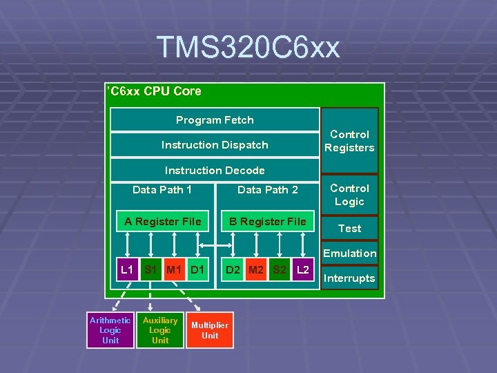 TMS 320 C 6 xx ’C 6 xx CPU Core Program Fetch Instruction Dispatch Control Registers Instruction Decode Data Path 1 Data Path 2 A Register File B Register File Control Logic Test Emulation L 1 S 1 M 1 D 1 Arithmetic Logic Unit Auxiliary Logic Unit D 2 M 2 S 2 L 2 Multiplier Unit Interrupts
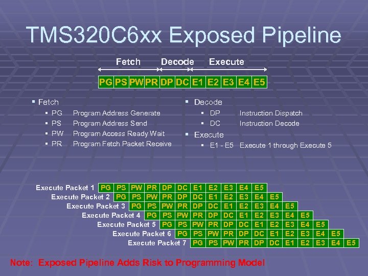 TMS 320 C 6 xx Exposed Pipeline Fetch Decode Execute PG PS PW PR DP DC E 1 E 2 E 3 E 4 E 5 § Fetch § § PG PS PW PR § Decode Program Address Generate Program Address Send Program Access Ready Wait Program Fetch Packet Receive § DP § DC Instruction Dispatch Instruction Decode § Execute Packet 1 PG PS PW PR DP DC Execute Packet 2 PG PS PW PR DP Execute Packet 3 PG PS PW PR Execute Packet 4 PG PS PW Execute Packet 5 PG PS Execute Packet 6 PG Execute Packet 7 § E 1 - E 5 Execute 1 through Execute 5 E 1 DC DP PR PW PS PG E 2 E 1 DC DP PR PW PS E 3 E 2 E 1 DC DP PR PW E 4 E 3 E 2 E 1 DC DP PR E 5 E 4 E 3 E 2 E 1 DC DP Note: Exposed Pipeline Adds Risk to Programming Model E 5 E 4 E 3 E 2 E 1 DC E 5 E 4 E 3 E 2 E 1 E 5 E 4 E 5 E 3 E 4 E 5 E 2 E 3 E 4 E 5
 Agenda § Industry Trends § DSP Architecture § DSP Micro-Architecture § DSP Systems
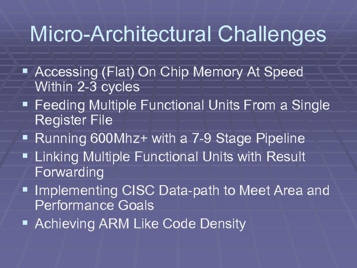 Micro-Architectural Challenges § Accessing (Flat) On Chip Memory At Speed § § § Within 2 -3 cycles Feeding Multiple Functional Units From a Single Register File Running 600 Mhz+ with a 7 -9 Stage Pipeline Linking Multiple Functional Units with Result Forwarding Implementing CISC Data-path to Meet Area and Performance Goals Achieving ARM Like Code Density
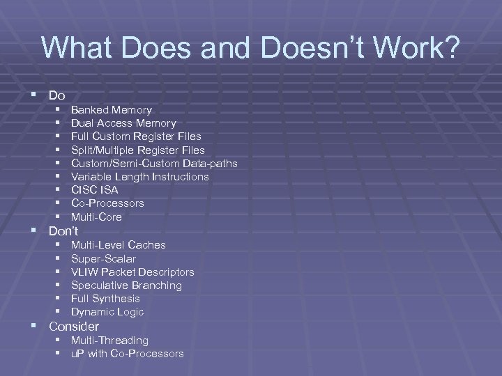 What Does and Doesn’t Work? § Do § § § § § Banked Memory Dual Access Memory Full Custom Register Files Split/Multiple Register Files Custom/Semi-Custom Data-paths Variable Length Instructions CISC ISA Co-Processors Multi-Core § § § Multi-Level Caches Super-Scalar VLIW Packet Descriptors Speculative Branching Full Synthesis Dynamic Logic § Don’t § Consider § Multi-Threading § u. P with Co-Processors
 Agenda § Industry Trends § DSP Architecture § DSP Micro-Architecture § DSP Systems
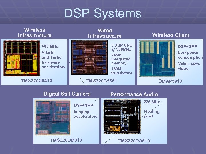 DSP Systems Wireless Infrastructure Wired. Infrastructure Performance Audio Digital Still Client Wireless Camera Wireless Infrastructure 6 DSP CPU 600 MHz Viterbi and Turbo hardware accelerators Wireless Client @ 300 MHz CPU 6225 MHz DSP+GPP 24 Mb 3 MB 300 MHz DSP+GPP @ integrated Imaging 600 MHz memory integrated Floating Low power 3 MB accelerators 180 M point consumption memory transistors Viterbi Voice, data, video hardware accelerators Performance Audio DSP+GPP Low power consumption Voice, data, video 180 M transistors and Turbo TMS 320 C 5561 OMAP 5910 TMS 320 C 6416 Digital Still Camera DSP+GPP Imaging TMS 320 C 5561 accelerators TMS 320 DM 310 TMS 320 DA 610 OMAP 5910 TMS 320 C 6416 TMS 320 DM 310 225 MHz Floating point TMS 320 DA 610
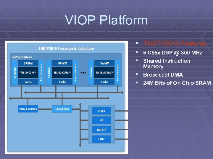 VIOP Platform § TNETV 3010 Features § 6 C 55 x DSP @ 300 MHz § Shared Instruction Memory § Broadcast DMA § 24 M Bits of On Chip SRAM
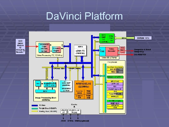 Da. Vinci Platform
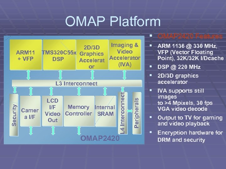 OMAP Platform § OMAP 2420 Features ARM 11 + VFP Imaging & 2 D/3 D Video TMS 320 C 55 x Graphics DSP Accelerator (IVA) or § DSP @ 220 MHz § 2 D/3 D graphics OMAP 2420 § IVA supports still Peripherals L 4 Interconnect Security Camer a I/F VFP (Vector Floating Point), 32 K/32 K I/Dcache accelerator L 3 Interconnect LCD Memory Internal I/F Video Controller SRAM Out § ARM 1136 @ 330 MHz, images to >4 Mpixels, 30 fps VGA video decode § Output to TV for gaming and video playback § Encryption hardware for DRM and security


