535389795639b76bd88387bab1c232f0.ppt
- Количество слайдов: 29
 Superconductor Technologies for Extreme Computing Arnold Silver A. Silver Workshop on Frontiers of Extreme Computing Monday, October 24, 2005 Santa Cruz, CA 1
 Outline Ø Introduction Ø Single Flux Quantum (SFQ) Technology Ø State-of-the-Art Ø Prospects Ø Quantum Computing Ø Summary A. Silver 2
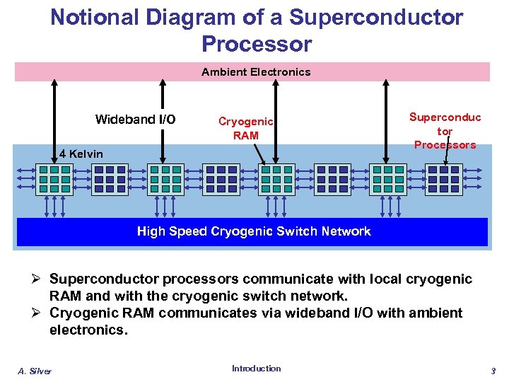 Notional Diagram of a Superconductor Processor Ambient Electronics Wideband I/O Cryogenic RAM 4 Kelvin Superconduc tor Processors High Speed Cryogenic Switch Network Ø Superconductor processors communicate with local cryogenic RAM and with the cryogenic switch network. Ø Cryogenic RAM communicates via wideband I/O with ambient electronics. A. Silver Introduction 3
 Early Technology Limited Ø Early superconductor logic was voltagelatching – Voltage state data – AC power required – Speed limited by RC load and reset time (~GHz) Ø Single Flux Quantum (SFQ) is latest generation. – – Current/Flux state data SFQ pulses transfer data DC powered Higher speed (~100 GHz) Ø Incremental progress on Do. D contracts. – Small annual budgets – Focus on small circuit demos – Minimal infrastructure investment A. Silver Introduction 4
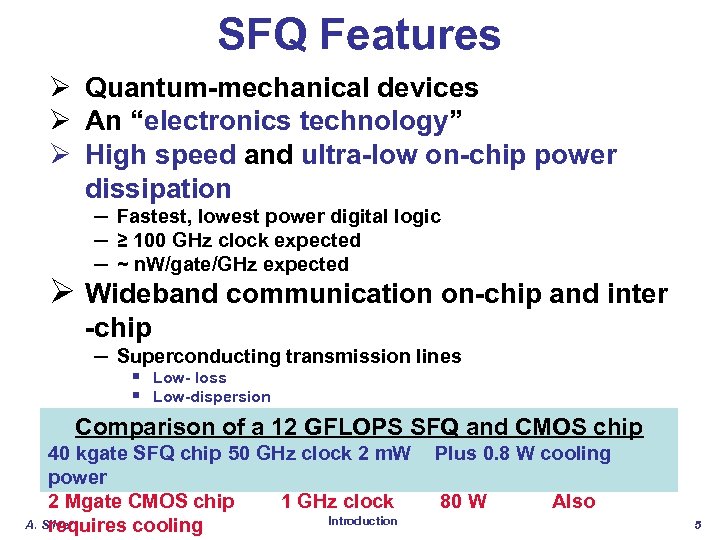 SFQ Features Ø Quantum-mechanical devices Ø An “electronics technology” Ø High speed and ultra-low on-chip power dissipation – Fastest, lowest power digital logic – ≥ 100 GHz clock expected – ~ n. W/gate/GHz expected Ø Wideband communication on-chip and inter -chip – Superconducting transmission lines § Low- loss § Low-dispersion § Impedance matched Comparison of a 12 GFLOPS SFQ and CMOS chip – 60 GHz data transfer demonstrated with negligible cross 40 kgate SFQ chip 50 GHz clock 2 m. W Plus 0. 8 W cooling talk power 2 Mgate CMOS chip 1 GHz clock 80 W Also Introduction A. Silver requires cooling 5
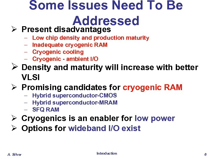 Some Issues Need To Be Addressed Ø Present disadvantages – – Low chip density and production maturity Inadequate cryogenic RAM Cryogenic cooling Cryogenic - ambient I/O Ø Density and maturity will increase with better VLSI Ø Promising candidates for cryogenic RAM – Hybrid superconductor-CMOS – Hybrid superconductor-MRAM – SFQ RAM Ø Cryogenics is an enabler for low power Ø Options for wideband I/O exist A. Silver Introduction 6
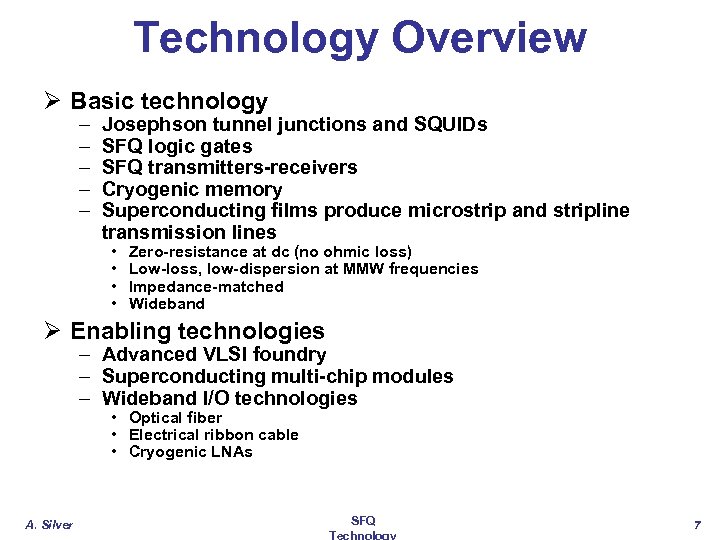 Technology Overview Ø Basic technology – – – Josephson tunnel junctions and SQUIDs SFQ logic gates SFQ transmitters-receivers Cryogenic memory Superconducting films produce microstrip and stripline transmission lines • • Zero-resistance at dc (no ohmic loss) Low-loss, low-dispersion at MMW frequencies Impedance-matched Wideband Ø Enabling technologies – Advanced VLSI foundry – Superconducting multi-chip modules – Wideband I/O technologies • Optical fiber • Electrical ribbon cable • Cryogenic LNAs A. Silver SFQ Technology 7
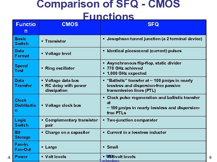 Functio n Comparison of SFQ - CMOS Functions CMOS Basic Switch § Transistor Data Format § Voltage level SFQ § Josephson tunnel junction (a 2 terminal device) § Identical picosecond (current) pulses § Ring oscillator § Asynchronous flip-flop, static divider § 770 GHz achieved § 1, 000 GHz expected § Voltage data bus § RC delay with power dissipation § “Ballistic” transfer at ~ 100 m/ps in nearly lossless and dispersion-free passive transmission lines (PTL) Clock Distributio n § Voltage clock bus § Clock pulse regeneration and ballistic transfer at ~ 100 m/ps in nearly lossless and dispersionfree PTLs Logic Switch § Complementary transistor § Two-junction comparator pair Bit Storage § Charge on a capacitor § Current in a lossless inductor § Large § Small Speed Test Data Transfer Fan-In, Fan-Out Power A. Silver § Volt levels § SFQ Millivolt levels Technology 8
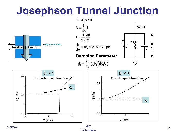 C ur r en t Josephson Tunnel Junction q Insulator (~1 nm) Magnetic field Damping Parameter bc > 1 bc < 1 IC IC A. Silver SFQ Technology 9
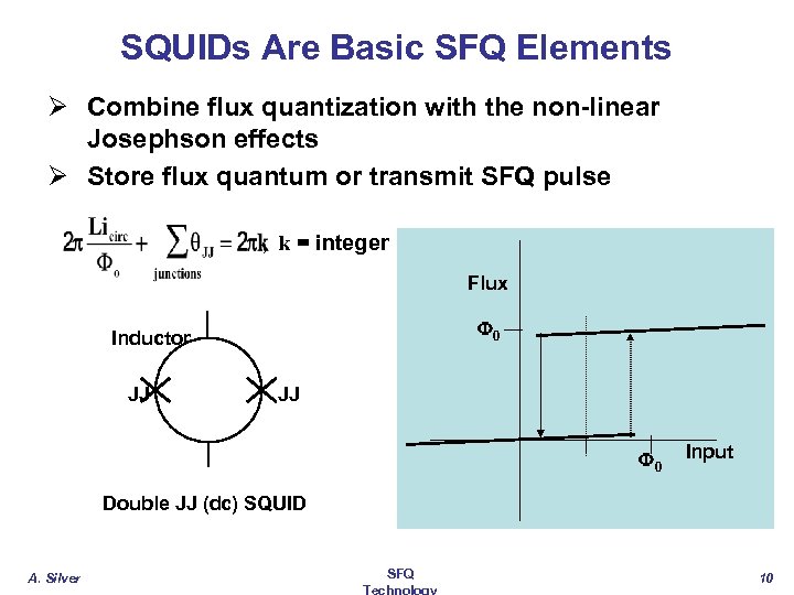 SQUIDs Are Basic SFQ Elements Ø Combine flux quantization with the non-linear Josephson effects Ø Store flux quantum or transmit SFQ pulse ; k = integer Flux F 0 Inductor JJ JJ F 0 Input Double JJ (dc) SQUID A. Silver SFQ Technology 10
 SFQ Is A Current Based Technology Ibias ~1 m. V Input JJ ~2 ps Ø When (Input + Ibias) exceeds JJ critical current Ic, JJ “flips”, producing an SFQ pulse. Ø Area of the pulse is F 0=2. 067 m. V-ps Ø Pulse width shrinks as JC increases Ø SFQ logic is based on counting single flux quanta A. Silver Ø SFQ pulses propagate along impedance-matched passive transmission line (PTL) at the speed of light in the line (~ c/3). Ø Multiple pulses can propagate in PTL simultaneously in both directions. SFQ Technology 11
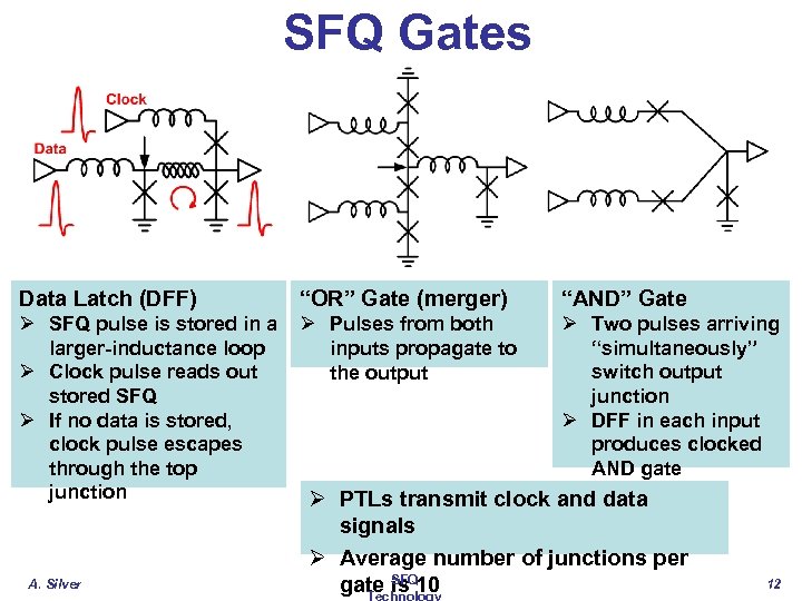 SFQ Gates Data Latch (DFF) “OR” Gate (merger) “AND” Gate Ø SFQ pulse is stored in a Ø Pulses from both Ø Two pulses arriving larger-inductance loop “simultaneously” inputs propagate to Ø Clock pulse reads out switch output the output stored SFQ junction Ø If no data is stored, Ø DFF in each input clock pulse escapes produces clocked through the top AND gate junction Ø PTLs transmit clock and data A. Silver signals Ø Average number of junctions per SFQ gate is 10 Technology 12
 Static Divider Speed (GHz) SFQ Is The Fastest Digital Technology Toggle Flip-Flop – Static Frequency Divider Ø Benchmark of SFQ circuit performance Ø Maximum frequency scales with JC ~2 m. V ~1 ps A. Silver 1000 NGST-Nb 300 NGST-Nb. N HYPRES SUNY 100 1 10 JC (k. A/cm 2) 100 Ø Measured dc to 446 GHz static divider Ø 770 GHz demonstrated in experiment Picosecond SFQ pulses can encode terabits per second. SFQ Technology 13
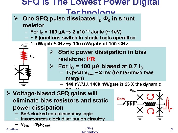 SFQ Is The Lowest Power Digital Technology Ø One SFQ pulse dissipates IC F 0 in shunt resistor – For IC = 100 A 2 x 10 -19 Joule (~ 1 e. V) – ~ 5 junctions switch in single logic operation – Vbias 1 n. W/gate/GHz 100 n. W/gate at 100 GHz Ibias Ø Static power dissipation in bias resistors: I 2 R Ø For IC = 100 A biased at 0. 7 IC – Typical Vbias = 2 m. V (to maximize bias margin) – 140 n. W/JJ, 1400 n. W/gate is 23 X the dynamic power Vbias Ø Voltage-biased SFQ gates will eliminate bias resistors and static power dissipation Data – Self-clocked complementary logic – Incorporates clock distribution circuitry – Vbias = F 0 FClock A. Silver SFQ Technology 14
 SFQ Digital ICs Have Been Developed Ø First SFQ circuit (~ 1977) was a dc to SFQ converter integrated with toggle flip-flops to form a binary counter. Ø Extensive development of SFQ logic did not occur until after 1990. Ø Advanced SFQ logic was developed on HTMT FLUX. – – – – A. Silver Architecture Design tools LSI fabrication Logic High data-rate on-chip communications Inter-chip communications Vector registers Microprocessor logic chip State-of-the-Art 15
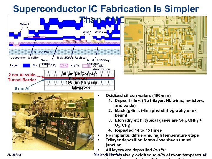 Superconductor IC Fabrication Is Simpler Than CMOS Wire 3 Wire 2 Wire 1 Wire 2 Silicon Wafer Josephson Junction Legend: Nb 2 nm Al oxide Tunnel Barrier 8 nm Al Ground Plane Si. O 2 Mo. Nx 5 /sq. Resistor Mo/Al 0. 15Ω/sq. Resistor Nb 2 O 5 Junction Anodization 100 nm Nb Counter Electrode 150 nm Nb Base Electrode Oxide § A. Silver Oxidized silicon wafers (100 -mm) 1. Deposit films (Nb trilayer, Nb wires, resistors, and oxide) 2. Mask (g-line, i-line photolithography or ebeam) 3. Etch (dry etch, typical gases are SF 6, CHF 3 + O 2, CF 4) 4. Repeated 14 to 15 times § No implants, diffusions, high temperature steps § Trilayer deposition forms Josephson tunnel junction § All layers are deposited in-situ State-of-the-Art 16 § Al is passively oxidized in-situ at room temperature
 Cadence-based SFQ Design Flow (NGST) Is similar to Semiconductor Design Logic Synthesis & Verification VHDL DRC Schematic RSFQ Gate Library LVS Layout Gate PCells LMeter Schematic Symbol Malt WRSpice Layout VHDL Generic Netlist A. Silver VHDL Structure State-of-the-Art 17
 Complex Chips Have Been Reported A. Silver State-of-the-Art 18
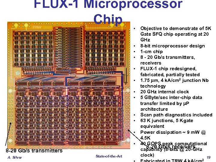 FLUX-1 Microprocessor Chip • • • 8 -20 Gb/s transmitters A. Silver State-of-the-Art Objective to demonstrate of 5 K Gate SFQ chip operating at 20 GHz 8 -bit microprocessor design 1 -cm chip 8 - 20 Gb/s transmitters, receivers FLUX-1 chip redesigned, fabricated, partially tested 1. 75 m, 4 k. A/cm 2 junction Nb technology 20 GHz internal clock 5 GByte/sec inter-chip data transfer limited by P architecture Scan path diagnostics included 63 K junctions, 5 Kgate equivalent Power dissipation ~ 9 m. W @ 4. 5 K 40 GOPS peak computational 8 -20 Gb/s receivers capability (8 -bits @ 20 -GHz clock) 19 2
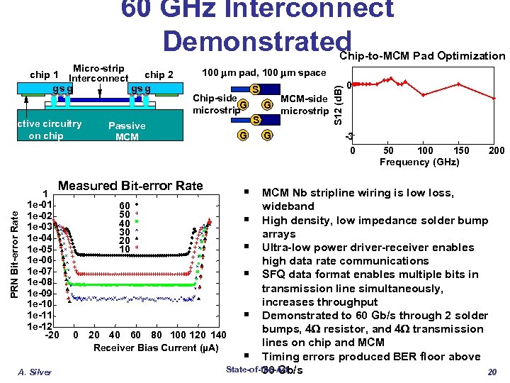 60 GHz Interconnect Demonstrated Chip-to-MCM Pad Optimization Active circuitry on chip 100 m pad, 100 m space Chip-side G microstrip Passive MCM PRN Bit-error Rate Measured Bit-error Rate 1 1 e-02 1 e-03 1 e-04 1 e-05 1 e-06 1 e-07 1 e-08 1 e-09 1 e-10 1 e-11 1 e-12 -20 A. Silver G S G MCM-side microstrip S 12 (d. B) Micro-strip chip 1 Interconnect chip 2 gs g gsg 0 -3 0 50 100 150 Frequency (GHz) 200 § MCM Nb stripline wiring is low loss, wideband § High density, low impedance solder bump arrays § Ultra-low power driver-receiver enables high data rate communications § SFQ data format enables multiple bits in transmission line simultaneously, increases throughput § Demonstrated to 60 Gb/s through 2 solder bumps, 4 resistor, and 4 transmission 0 20 40 60 80 100 120 140 lines on chip and MCM Receiver Bias Current (µA) § Timing errors produced BER floor above State-of-the-Art 30 Gb/s 20 60 50 40 30 20 10
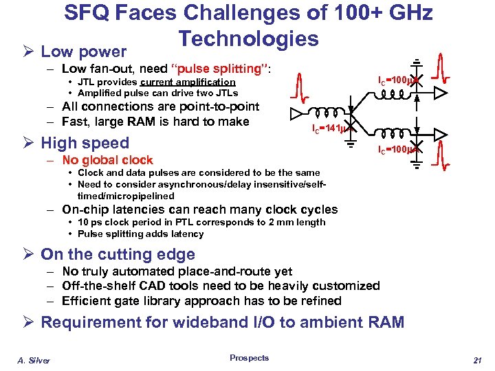 SFQ Faces Challenges of 100+ GHz Technologies Ø Low power – Low fan-out, need “pulse splitting”: IC=100 A • JTL provides current amplification • Amplified pulse can drive two JTLs – All connections are point-to-point – Fast, large RAM is hard to make Ø High speed IC=141 A IC=100 A – No global clock • Clock and data pulses are considered to be the same • Need to consider asynchronous/delay insensitive/selftimed/micropipelined – On-chip latencies can reach many clock cycles • 10 ps clock period in PTL corresponds to 2 mm length • Pulse splitting adds latency Ø On the cutting edge – No truly automated place-and-route yet – Off-the-shelf CAD tools need to be heavily customized – Efficient gate library approach has to be refined Ø Requirement for wideband I/O to ambient RAM A. Silver Prospects 21
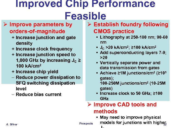 Improved Chip Performance Feasible Ø Improve parameters by orders-of-magnitude Ø Establish foundry following CMOS practice § Lithography at 250 -180 nm; 90 -60 nm § JC >20 k. A/cm 2; ≥ 100 k. A/cm 2 § Add superconducting layers 7 -9; >20 § Vertically separate power and data transmission from gates § Achieve ≥ 1 M junctions/cm 2 (≥ 105 gates); 100 -250 M junctions/cm 2 (10 -25 M gates) § Increase clock to 50 GHz; ≥ 100 GHz + Increase junction and gate density + Increase clock frequency + Increase junction speed to 1, 000 GHz by increasing JC ≥ 100 k. A/cm 2 + Increase chip yield – Reduce power dissipation to SFQ switching dissipation level – Reduce bias current Ø Improve CAD tools and methods A. Silver Prospects § May need to improve physical models for junctions with higher 22
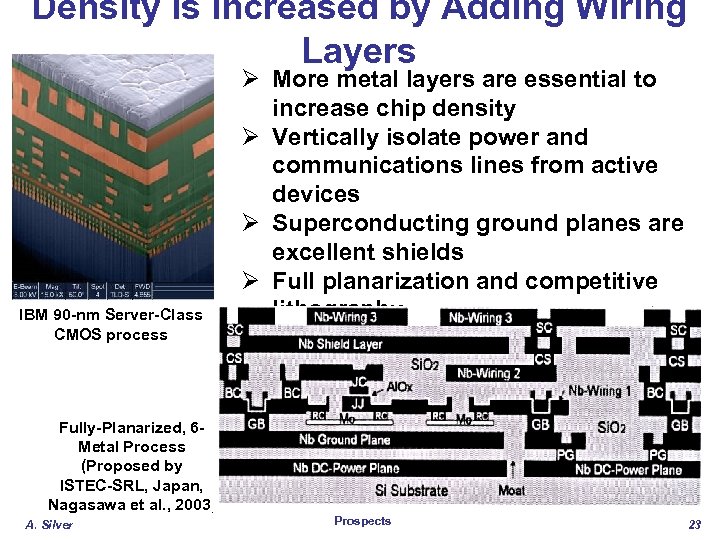 Density Is Increased by Adding Wiring Layers IBM 90 -nm Server-Class CMOS process Ø More metal layers are essential to increase chip density Ø Vertically isolate power and communications lines from active devices Ø Superconducting ground planes are excellent shields Ø Full planarization and competitive lithography Fully-Planarized, 6 Metal Process (Proposed by ISTEC-SRL, Japan, Nagasawa et al. , 2003) A. Silver Prospects 23
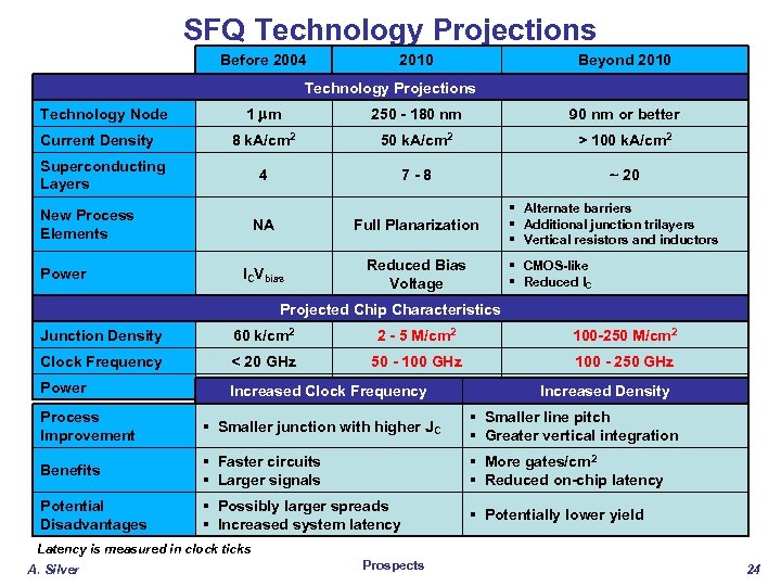 SFQ Technology Projections Before 2004 2010 Beyond 2010 Technology Projections Technology Node Current Density 1 m 250 - 180 nm 90 nm or better 8 k. A/cm 2 50 k. A/cm 2 > 100 k. A/cm 2 4 7 - 8 ~ 20 NA Full Planarization ICVbias Reduced Bias Voltage Superconducting Layers New Process Elements Power § Alternate barriers § Additional junction trilayers § Vertical resistors and inductors § CMOS-like § Reduced IC Projected Chip Characteristics Junction Density 60 k/cm 2 2 - 5 M/cm 2 100 -250 M/cm 2 Clock Frequency < 20 GHz 50 - 100 GHz 100 - 250 GHz Power 0. 2 W/Junction 8 n. W/GHz/Junction Increased Clock Frequency 0. 4 n. W/GHz/Junction Increased Density Process Improvement § Smaller junction with higher JC § Smaller line pitch § Greater vertical integration Benefits § Faster circuits § Larger signals § More gates/cm 2 § Reduced on-chip latency Potential Disadvantages § Possibly larger spreads § Increased system latency § Potentially lower yield Latency is measured in clock ticks A. Silver Prospects 24
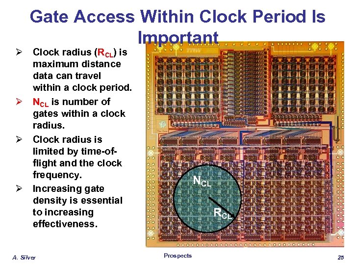 Gate Access Within Clock Period Is Important Ø Clock radius (RCL) is maximum distance data can travel within a clock period. Ø NCL is number of gates within a clock radius. Ø Clock radius is limited by time-offlight and the clock frequency. Ø Increasing gate density is essential to increasing effectiveness. A. Silver NCL RCL Prospects 25
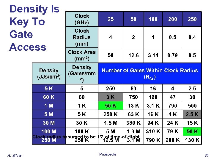 Density Is Key To Gate Access Clock (GHz) 25 50 100 250 Clock Radius (mm) 4 2 1 0. 5 0. 4 Clock Area (mm 2) 50 12. 6 3. 14 0. 79 0. 5 Density (JJs/cm 2) Density (Gates/mm 2) 5 K 5 250 63 16 4 2. 5 60 K 60 3 K 750 190 47 30 1 M 1 K 50 K 13 K 3. 1 K 790 500 5 M 5 K 250 K 63 K 16 K 4 K 2. 5 K 30 M 30 K 1. 5 M 380 K 94 K 24 K 15 K 100 M 100 K 5 M 1. 3 M 310 K 79 K 50 K 250 M 250 K 12. 5 M 3. 1 M 790 K 200 K 130 K Number of Gates Within Clock Radius (NCL) Clock radius assumed to be 1/2 of time-of-flight. A. Silver Prospects 26
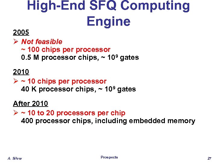 High-End SFQ Computing Engine 2005 Ø Not feasible ~ 100 chips per processor 0. 5 M processor chips, ~ 109 gates 2010 Ø ~ 10 chips per processor 40 K processor chips, ~ 109 gates After 2010 Ø ~ 10 to 20 processors per chip 400 processor chips, including embedded memory A. Silver Prospects 27
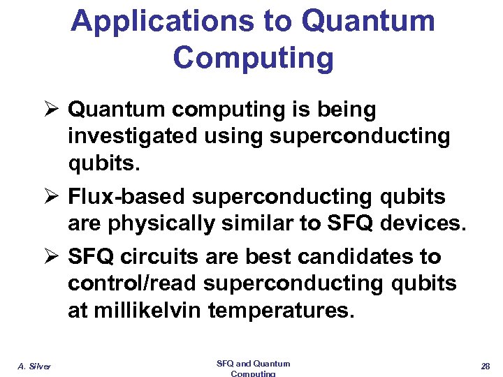 Applications to Quantum Computing Ø Quantum computing is being investigated using superconducting qubits. Ø Flux-based superconducting qubits are physically similar to SFQ devices. Ø SFQ circuits are best candidates to control/read superconducting qubits at millikelvin temperatures. A. Silver SFQ and Quantum Computing 28
 Summary Ø SFQ needs major engineering development in chip technology if it is going to be a player in high-end computing. Ø The engineering requirements are understood and a development plan defined. Ø Prospects are exciting and achievable. A. Silver Summary 29


