36841655b80b189a16fa32ad80c923d8.ppt
- Количество слайдов: 105
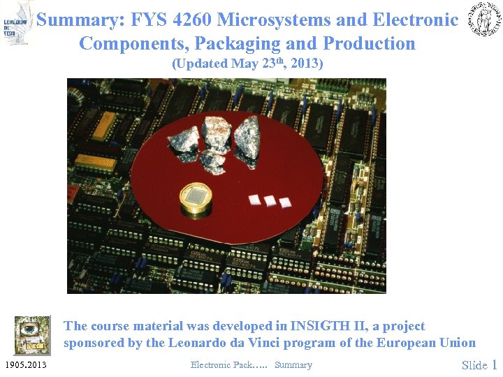 Summary: FYS 4260 Microsystems and Electronic Components, Packaging and Production (Updated May 23 th, 2013) The course material was developed in INSIGTH II, a project sponsored by the Leonardo da Vinci program of the European Union 1905. 2013 Electronic Pack…. . Summary Slide 1
 Compulsory Project • The Compulsory Projects were graded and will count 20% • Compulsory means compulsory – project report must be submitted and oral presentation must be given, and grading A, B, C, D or E necessary for final exam admission. • SMD Circuit Design, Production and Testing are important for the course and should be understood and learned – Questions usually given to check that all students in each group have worked with the project and understood and learned issues covered. Electronic Pack…. . Summary Slide 2
 Chapter 1 Introduction: Electronic products, technologies and packaging • Definition of ELECTRONIC PACKAGING: –"The realization of the physical, electronic system, starting with block-/circuit diagram” • Involves choice of technology for implementation, choice of materials, detailed design in chosen technology, analysis of electrical and thermal properties, reliability. • This definition is one among many, and may shift as the field is further developed. Electronic Pack…. . Summary Slide 3
 Multidisciplinary • Requires combination of many disciplines: – Electronics – Materials properties and materials compatibility – Mechanics – Chemistry – Metallurgy – Production technology – Reliability, etc. Electronic Pack…. . Summary Slide 4
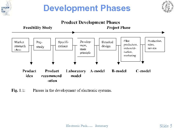 Development Phases Electronic Pack…. . Summary Slide 5
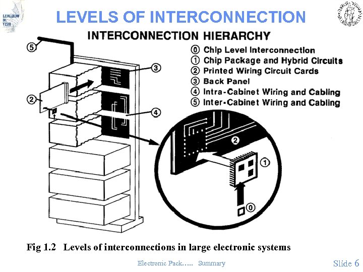 LEVELS OF INTERCONNECTION Fig 1. 2 Levels of interconnections in large electronic systems Electronic Pack…. . Summary Slide 6
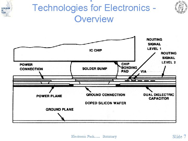 Chapter 2: Technologies for Electronics Overview Electronic Pack…. . Summary Slide 7
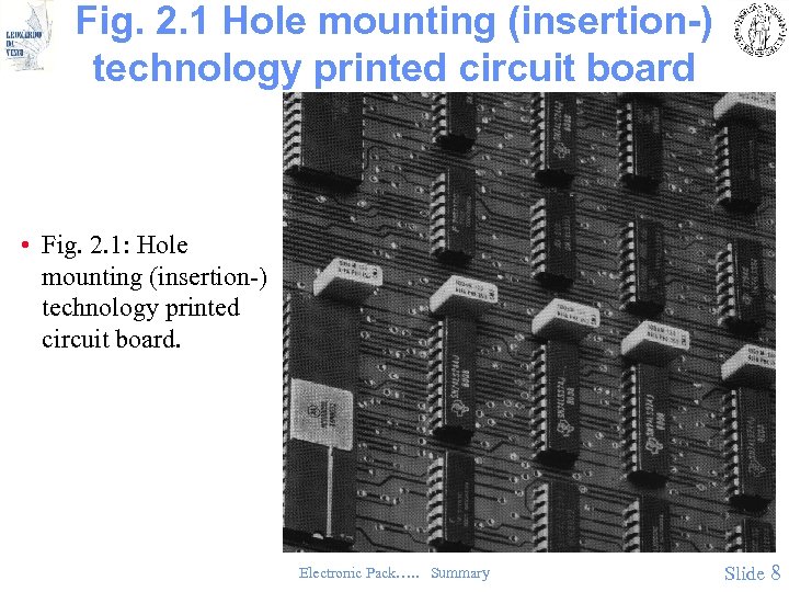 Fig. 2. 1 Hole mounting (insertion-) technology printed circuit board • Fig. 2. 1: Hole mounting (insertion-) technology printed circuit board. Electronic Pack…. . Summary Slide 8
 Fig. 2. 2 Surface mount technology printed circuit board • Fig. 2. 2: Surface mount technology printed circuit board. Electronic Pack…. . Summary Slide 9
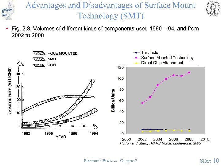 Advantages and Disadvantages of Surface Mount Technology (SMT) • Fig. 2. 3 Volumes of different kinds of components used 1980 – 94, and from 2002 to 2008 Electronic Pack…. . Chapter 2 Slide 10
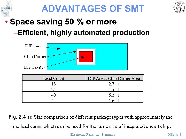 ADVANTAGES OF SMT • Space saving 50 % or more –Efficient, highly automated production Fig. 2. 4 a): Size comparison of different package types with approximately the same lead count which can be used for the same size of integrated circuit chip Electronic Pack…. . Summary . Slide 11
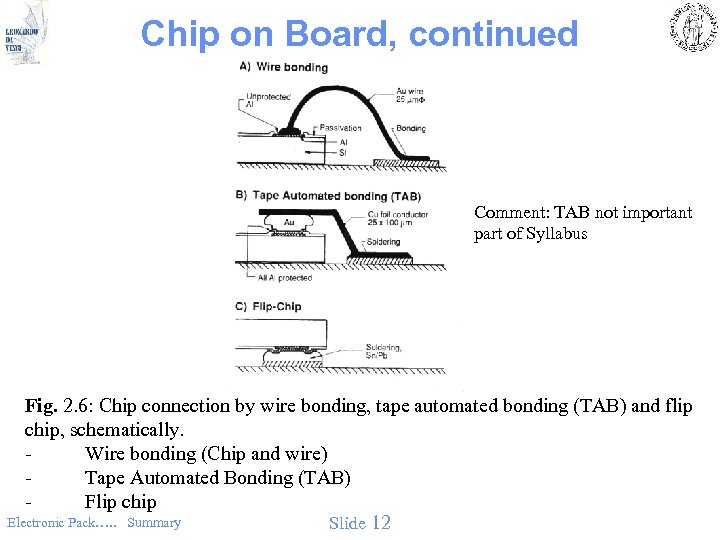 Chip on Board, continued Comment: TAB not important part of Syllabus Fig. 2. 6: Chip connection by wire bonding, tape automated bonding (TAB) and flip chip, schematically. Wire bonding (Chip and wire) Tape Automated Bonding (TAB) Flip chip Electronic Pack…. . Summary Slide 12
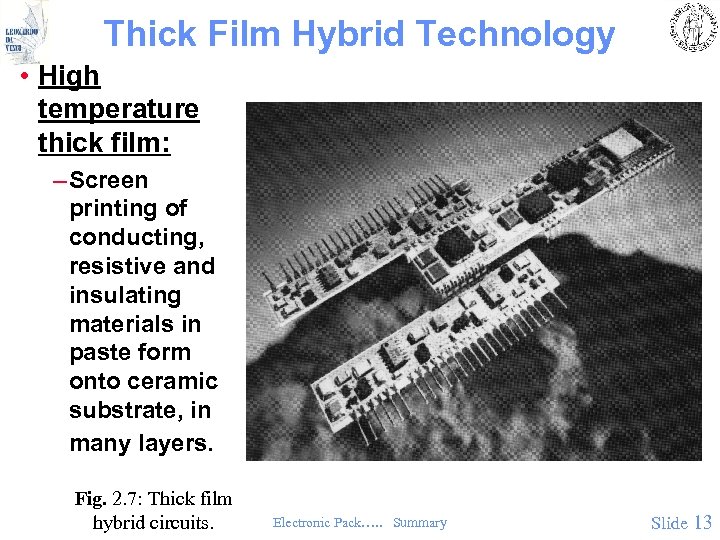 Thick Film Hybrid Technology • High temperature thick film: – Screen printing of conducting, resistive and insulating materials in paste form onto ceramic substrate, in many layers. Fig. 2. 7: Thick film hybrid circuits. Electronic Pack…. . Summary Slide 13
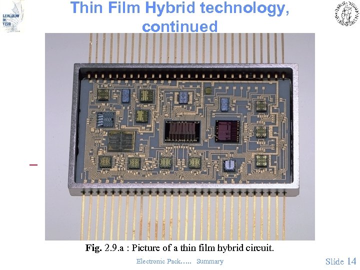 Thin Film Hybrid technology, continued (Fig. 2. 9) – Fig. 2. 9. a : Picture of a thin film hybrid circuit. Electronic Pack…. . Summary Slide 14
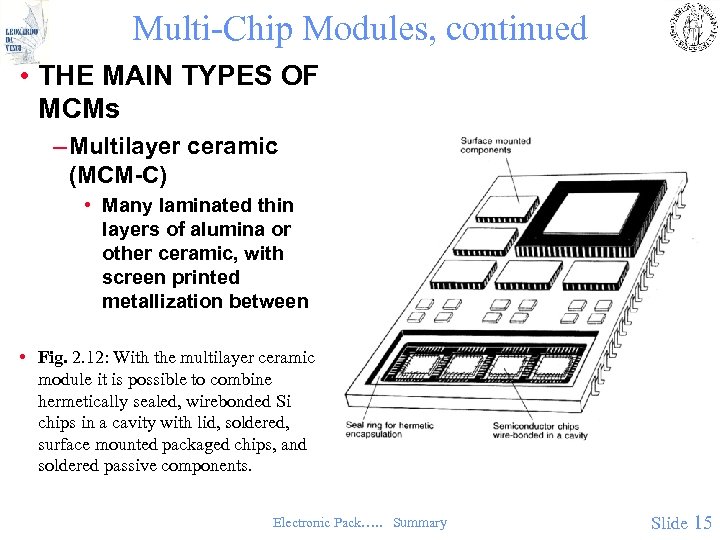 Multi-Chip Modules, continued • THE MAIN TYPES OF MCMs – Multilayer ceramic (MCM-C) • Many laminated thin layers of alumina or other ceramic, with screen printed metallization between • Fig. 2. 12: With the multilayer ceramic module it is possible to combine hermetically sealed, wirebonded Si chips in a cavity with lid, soldered, surface mounted packaged chips, and soldered passive components. Electronic Pack…. . Summary Slide 15
 TECHNOLOGY TRENDS • The development in semiconductor technology makes ever more advanced electronic systems possible. Some important trends for the systems development are: – Smaller critical dimensions, i. e. line widths and distances on the IC and module/PCB. – Increasing packaging density, i. e. more and more electric functions are possible to implement in a given area or volume – Increasing maximum operating frequency/bit rate – Increasing power dissipated per unit area and -volume – Increased possibility to realise complex circuit functions with standard hardware by programming software – Ever lower price per electrical function Electronic Pack…. . Summary Slide 16
 Technology Trends, continued • The established technology cannot satisfy the needs and requirements, and new technology always appears. It seems as if we hit physical limits on many fronts. • However, earlier, when such limits have appeared, new ideas and new principles have been found. • This will probably also happen in the future and will make the field of microelectronics dynamic and exciting in the future, for scientists as well as for users. Electronic Pack…. . Summary Slide 17
 Chapter 3 Materials and Basic processes Electronic Pack…. . Summary Slide 18
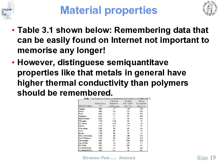 Material properties • Table 3. 1 shown below: Remembering data that can be easily found on Internet not important to memorise any longer! • However, distinguese semiquantitave properties like that metals in general have higher thermal conductivity than polymers should be remembered. Electronic Pack…. . Summary Slide 19
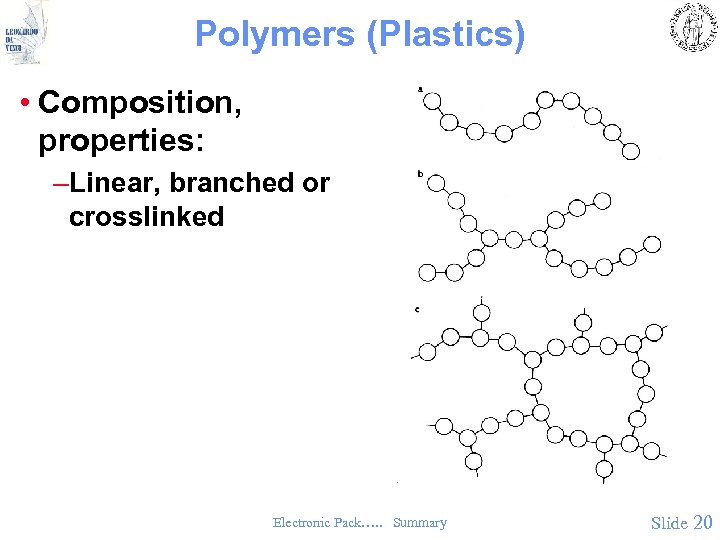 Polymers (Plastics) • Composition, properties: –Linear, branched or crosslinked Electronic Pack…. . Summary Slide 20
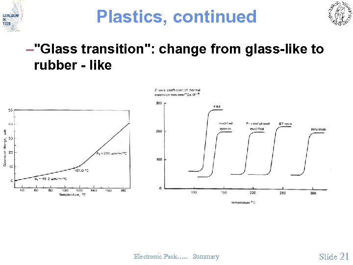 Plastics, continued –"Glass transition": change from glass-like to rubber - like Electronic Pack…. . Summary Slide 21
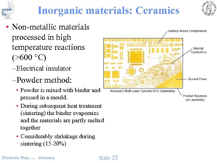 Inorganic materials: Ceramics • Non-metallic materials processed in high temperature reactions (>600 °C) – Electrical insulator –Powder method: • Powder is mixed with binder and pressed in a mould. • During subsequent heat treatment (sintering) the binder evaporates and the materials are partly melted together • Considerably shrinkage during sintering (15 -20%) Electronic Pack…. . Summary Slide 22
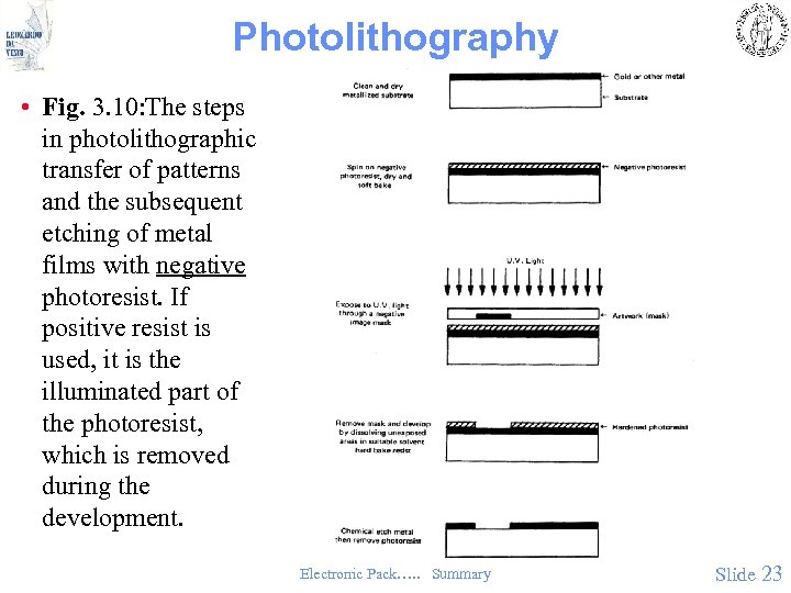 Photolithography • Fig. 3. 10: The steps in photolithographic transfer of patterns and the subsequent etching of metal films with negative photoresist. If positive resist is used, it is the illuminated part of the photoresist, which is removed during the development. Electronic Pack…. . Summary Slide 23
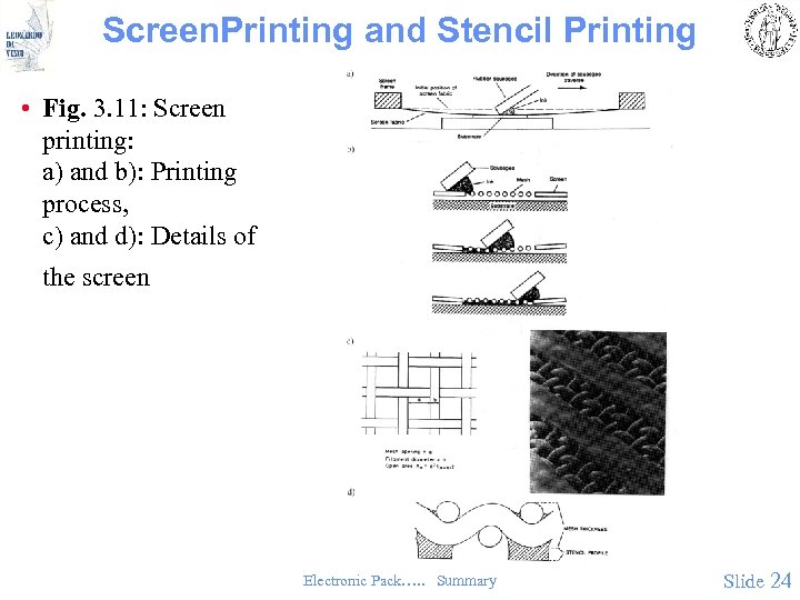 Screen. Printing and Stencil Printing • Fig. 3. 11: Screen printing: a) and b): Printing process, c) and d): Details of the screen Electronic Pack…. . Summary Slide 24
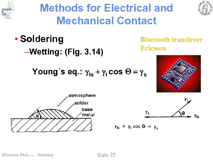 Methods for Electrical and Mechanical Contact • Soldering –Wetting: (Fig. 3. 14) Bluetooth tranciever Ericsson Young´s eq. : gls + gl cos Q = gs Electronic Pack…. . Summary Slide 25
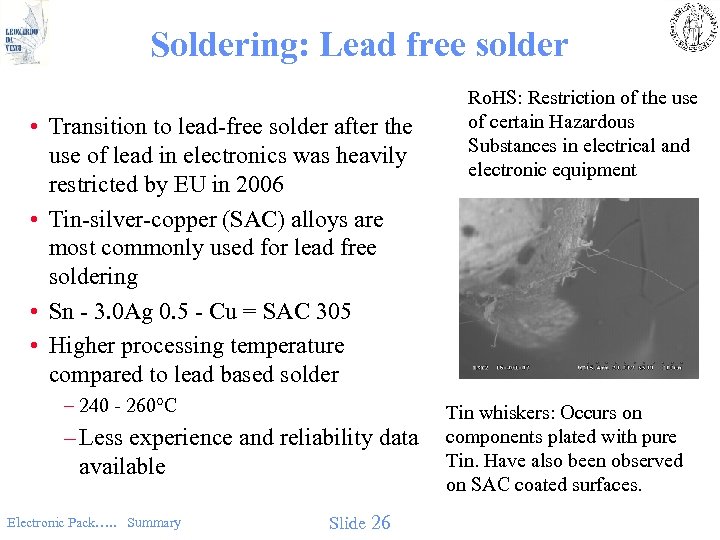 Soldering: Lead free solder • Transition to lead-free solder after the use of lead in electronics was heavily restricted by EU in 2006 • Tin-silver-copper (SAC) alloys are most commonly used for lead free soldering • Sn - 3. 0 Ag 0. 5 - Cu = SAC 305 • Higher processing temperature compared to lead based solder – 240 - 260°C – Less experience and reliability data available Electronic Pack…. . Summary Slide 26 Ro. HS: Restriction of the use of certain Hazardous Substances in electrical and electronic equipment Tin whiskers: Occurs on components plated with pure Tin. Have also been observed on SAC coated surfaces.
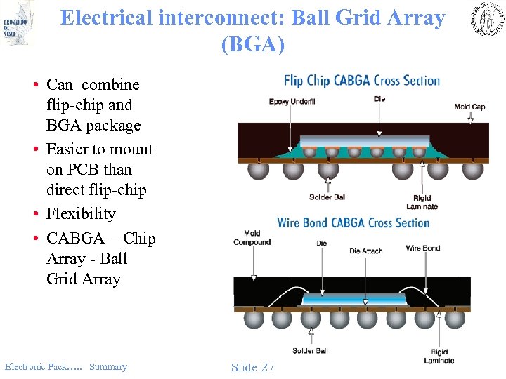 Electrical interconnect: Ball Grid Array (BGA) • Can combine flip-chip and BGA package • Easier to mount on PCB than direct flip-chip • Flexibility • CABGA = Chip Array - Ball Grid Array Electronic Pack…. . Summary Slide 27
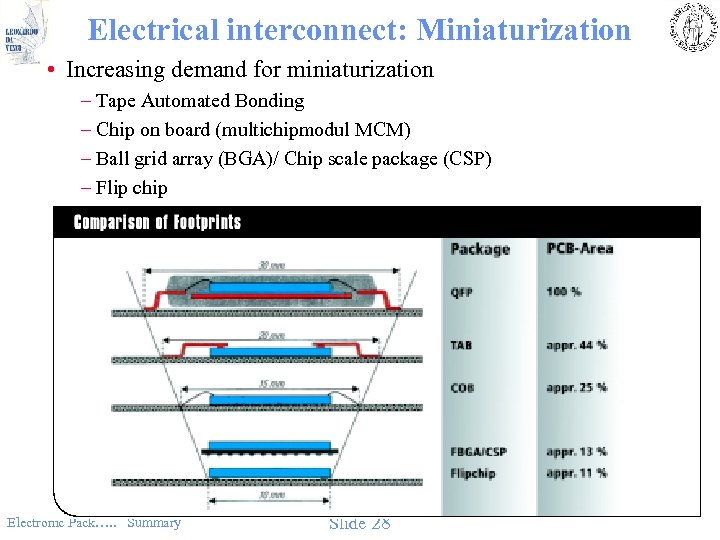 Electrical interconnect: Miniaturization • Increasing demand for miniaturization – Tape Automated Bonding – Chip on board (multichipmodul MCM) – Ball grid array (BGA)/ Chip scale package (CSP) – Flip chip Electronic Pack…. . Summary Slide 28
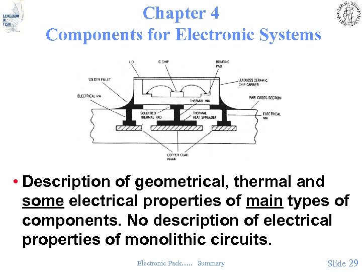 Chapter 4 Components for Electronic Systems • Description of geometrical, thermal and some electrical properties of main types of components. No description of electrical properties of monolithic circuits. Electronic Pack…. . Summary Slide 29
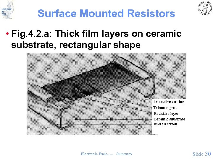 Surface Mounted Resistors • Fig. 4. 2. a: Thick film layers on ceramic substrate, rectangular shape Electronic Pack…. . Summary Slide 30
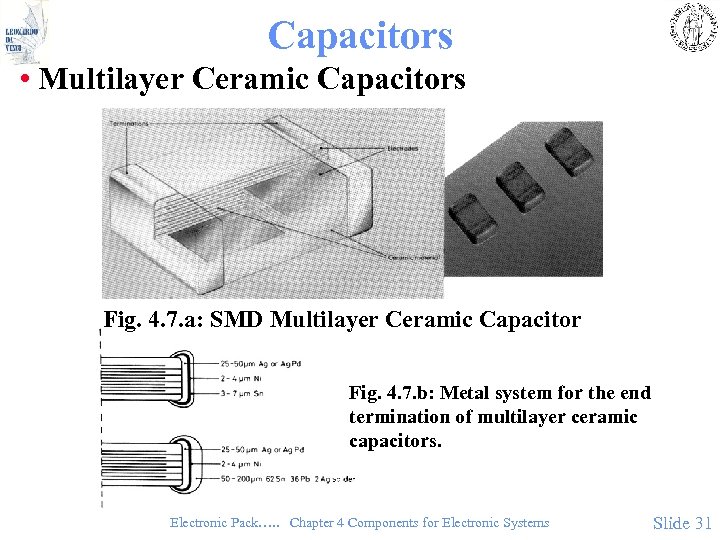 Capacitors • Multilayer Ceramic Capacitors Fig. 4. 7. a: SMD Multilayer Ceramic Capacitor Fig. 4. 7. b: Metal system for the end termination of multilayer ceramic capacitors. Electronic Pack…. . Chapter 4 Components for Electronic Systems Slide 31
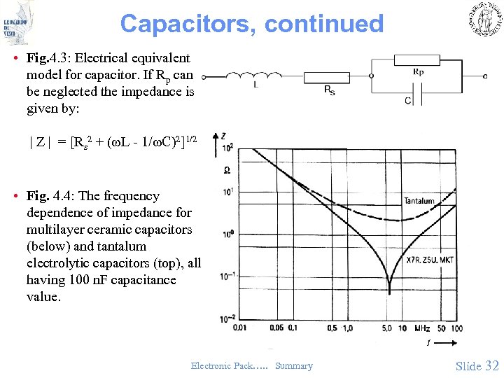 Capacitors, continued • Fig. 4. 3: Electrical equivalent model for capacitor. If Rp can be neglected the impedance is given by: | Z | = [Rs 2 + (w. L - 1/w. C)2]1/2 • Fig. 4. 4: The frequency dependence of impedance for multilayer ceramic capacitors (below) and tantalum electrolytic capacitors (top), all having 100 n. F capacitance value. Electronic Pack…. . Summary Slide 32
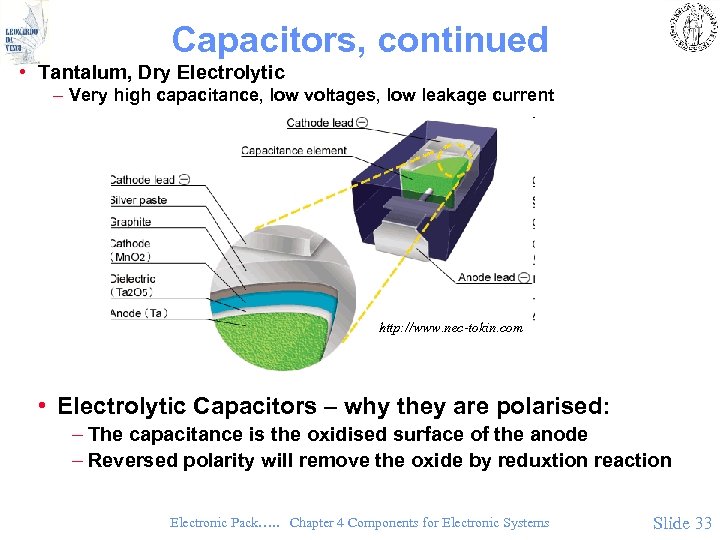 Capacitors, continued • Tantalum, Dry Electrolytic – Very high capacitance, low voltages, low leakage current http: //www. nec-tokin. com • Electrolytic Capacitors – why they are polarised: – The capacitance is the oxidised surface of the anode – Reversed polarity will remove the oxide by reduxtion reaction Electronic Pack…. . Chapter 4 Components for Electronic Systems Slide 33
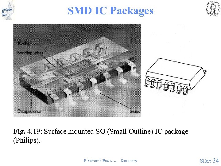 SMD IC Packages Fig. 4. 19: Surface mounted SO (Small Outline) IC package (Philips). Electronic Pack…. . Summary Slide 34
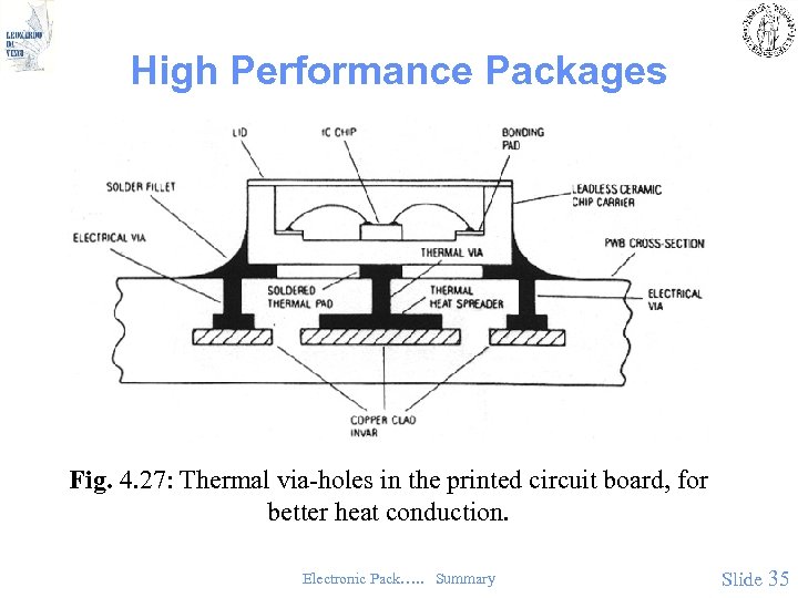 High Performance Packages Fig. 4. 27: Thermal via-holes in the printed circuit board, for better heat conduction. Electronic Pack…. . Summary Slide 35
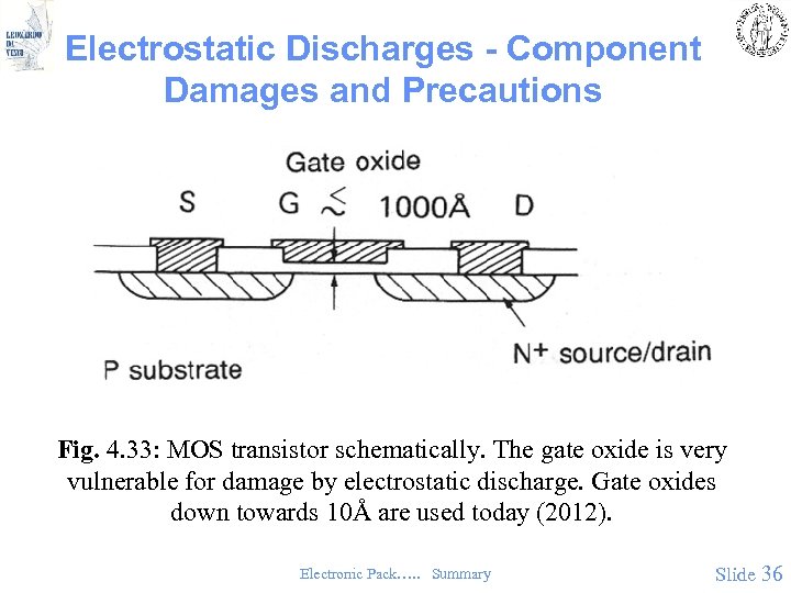 Electrostatic Discharges - Component Damages and Precautions Fig. 4. 33: MOS transistor schematically. The gate oxide is very vulnerable for damage by electrostatic discharge. Gate oxides down towards 10Å are used today (2012). Electronic Pack…. . Summary Slide 36
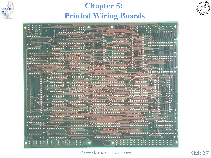 Chapter 5: Printed Wiring Boards Electronic Pack…. . Summary Slide 37
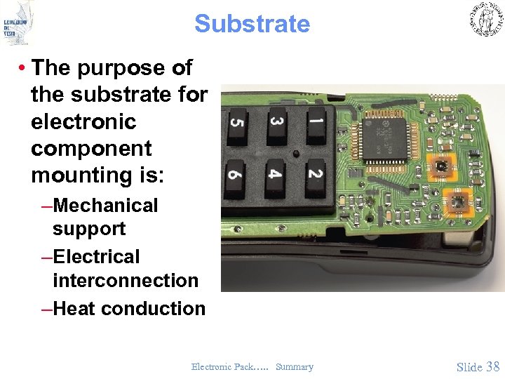 Substrate • The purpose of the substrate for electronic component mounting is: –Mechanical support –Electrical interconnection –Heat conduction Electronic Pack…. . Summary Slide 38
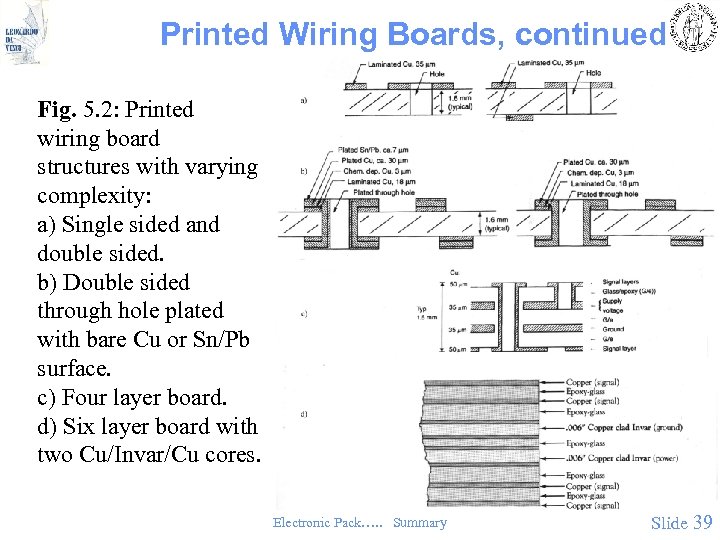 Printed Wiring Boards, continued Fig. 5. 2: Printed wiring board structures with varying complexity: a) Single sided and double sided. b) Double sided through hole plated with bare Cu or Sn/Pb surface. c) Four layer board. d) Six layer board with two Cu/Invar/Cu cores. Electronic Pack…. . Summary Slide 39
 New Materials for PWBs • • • Higher Tg Better dimensional stability er low, not dependent on T, f, or moisture Low losses Lower TCE Purpose – High frequency use – Controlled characteristic impedance – High reliability • Materials – Cyanate ester – PTFE (Teflon) – Polyimide – and others Electronic Pack…. . Summary Slide 40
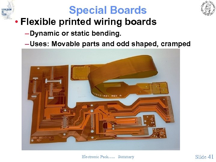 Special Boards • Flexible printed wiring boards – Dynamic or static bending. – Uses: Movable parts and odd shaped, cramped places Electronic Pack…. . Summary Slide 41
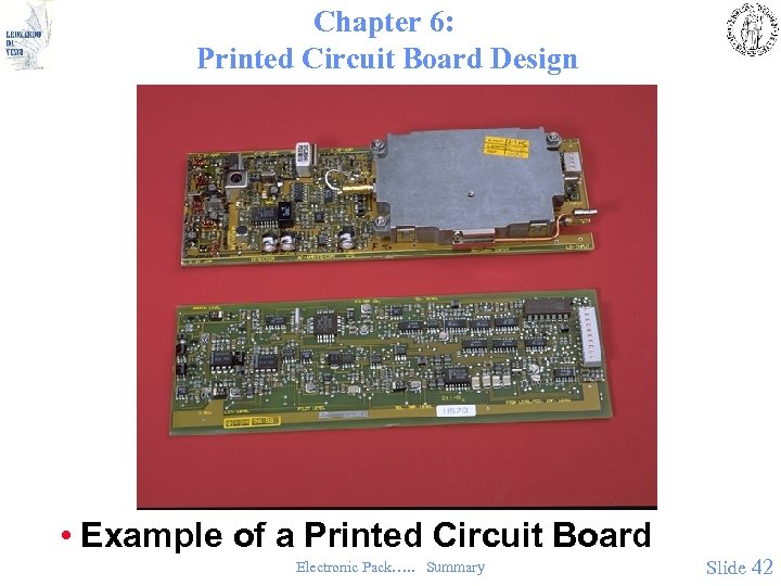 Chapter 6: Printed Circuit Board Design • Example of a Printed Circuit Board Electronic Pack…. . Summary Slide 42
 PCB Design, continued • Advanced PCB CAD tools a neccessity –Schematics –Component Library –Critical Parameters (Placement Constraints, Electromagnetic Compatibility, Thermal Limitations, etc) –Automatic Routing –Final Touch Manual Routing –(Verification by Final Simulation and Back Annotation) Electronic Pack…. . Summary Slide 43
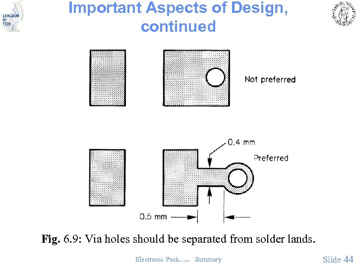 Important Aspects of Design, continued Fig. 6. 9: Via holes should be separated from solder lands. Electronic Pack…. . Summary Slide 44
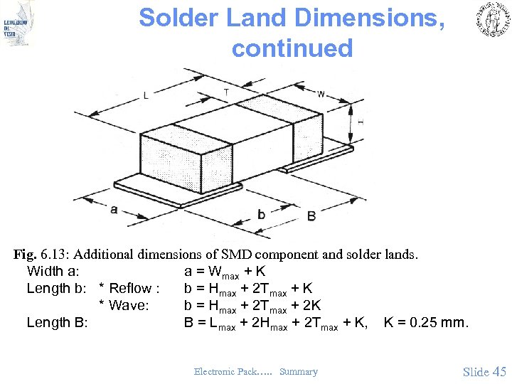 Solder Land Dimensions, continued Fig. 6. 13: Additional dimensions of SMD component and solder lands. Width a: a = Wmax + K Length b: * Reflow : b = Hmax + 2 Tmax + K * Wave: b = Hmax + 2 Tmax + 2 K Length B: B = Lmax + 2 Hmax + 2 Tmax + K, K = 0. 25 mm. Electronic Pack…. . Summary Slide 45
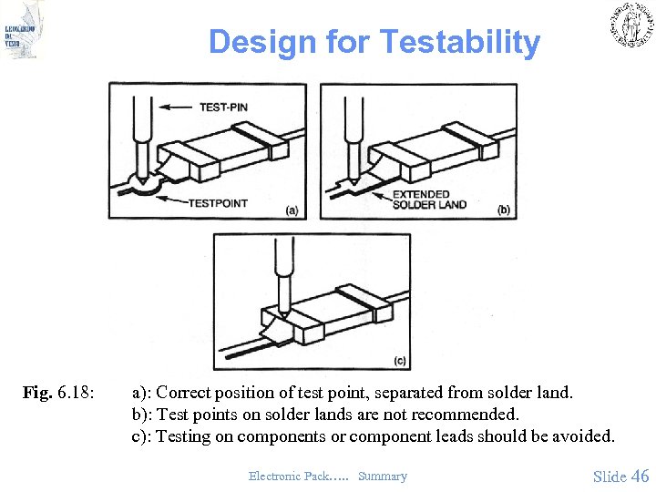 Design for Testability Fig. 6. 18: a): Correct position of test point, separated from solder land. b): Test points on solder lands are not recommended. c): Testing on components or component leads should be avoided. Electronic Pack…. . Summary Slide 46
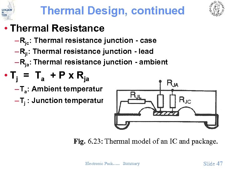 Thermal Design, continued • Thermal Resistance – Rjc: Thermal resistance junction - case – Rjl: Thermal resistance junction - lead – Rja: Thermal resistance junction - ambient • Tj = Ta + P x Rja – Ta: Ambient temperature – Tj : Junction temperature Fig. 6. 23: Thermal model of an IC and package. Electronic Pack…. . Summary Slide 47
 High Frequency Design • When needed? –tr < 2. 5 tf –tr = 10 - 90 % rise time –tf = l/v • tr is 10 -90% rise time • tf is time-of-flight-delay over the length l of critical conductor paths of the circuit • v is propagation speed: v = c/ er – c speed of light – er effective relative dielectric constant Electronic Pack…. . Summary Slide 48
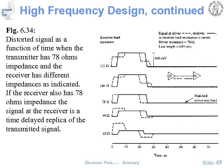 High Frequency Design, continued Fig. 6. 34: Distorted signal as a function of time when the transmitter has 78 ohms impedance and the receiver has different impedances as indicated. If the receiver also has 78 ohms impedance the signal at the receiver is a time delayed replica of the transmitted signal. Electronic Pack…. . Summary Slide 49
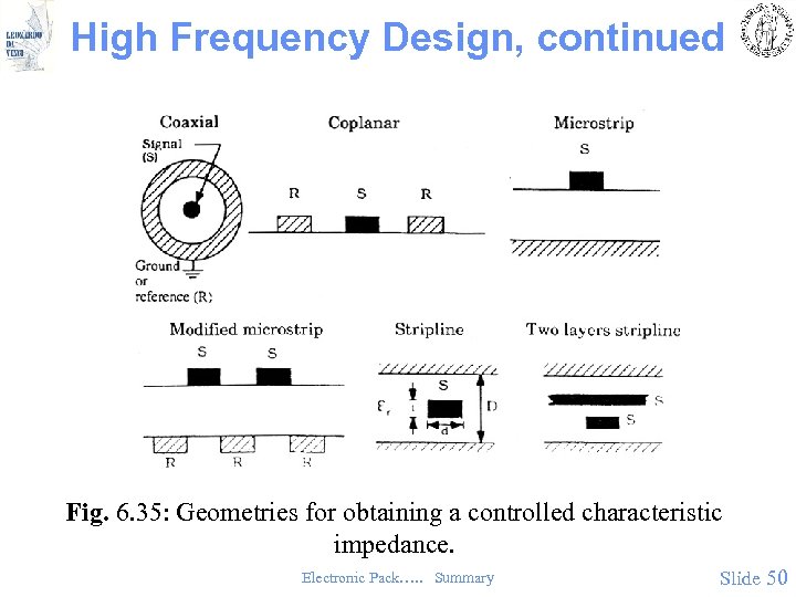 High Frequency Design, continued Fig. 6. 35: Geometries for obtaining a controlled characteristic impedance. Electronic Pack…. . Summary Slide 50
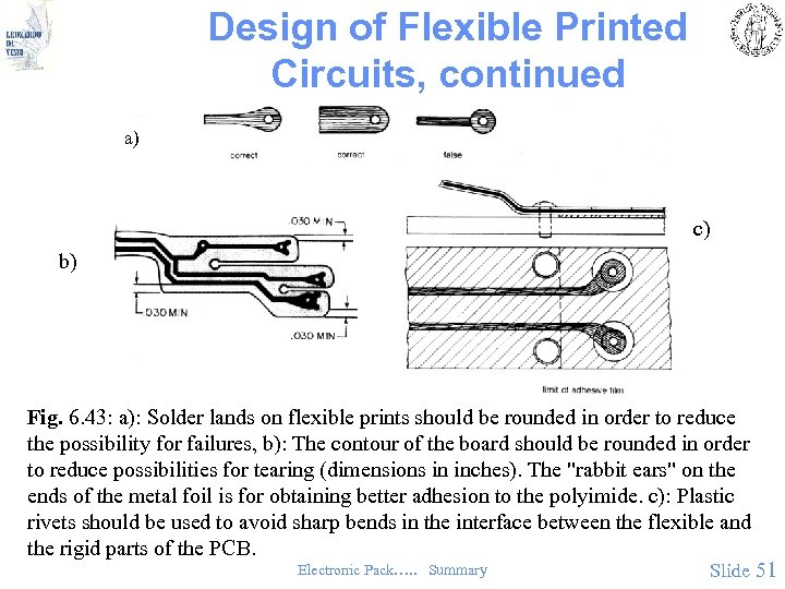 Design of Flexible Printed Circuits, continued a) c) b) Fig. 6. 43: a): Solder lands on flexible prints should be rounded in order to reduce the possibility for failures, b): The contour of the board should be rounded in order to reduce possibilities for tearing (dimensions in inches). The "rabbit ears" on the ends of the metal foil is for obtaining better adhesion to the polyimide. c): Plastic rivets should be used to avoid sharp bends in the interface between the flexible and the rigid parts of the PCB. Electronic Pack…. . Summary Slide 51
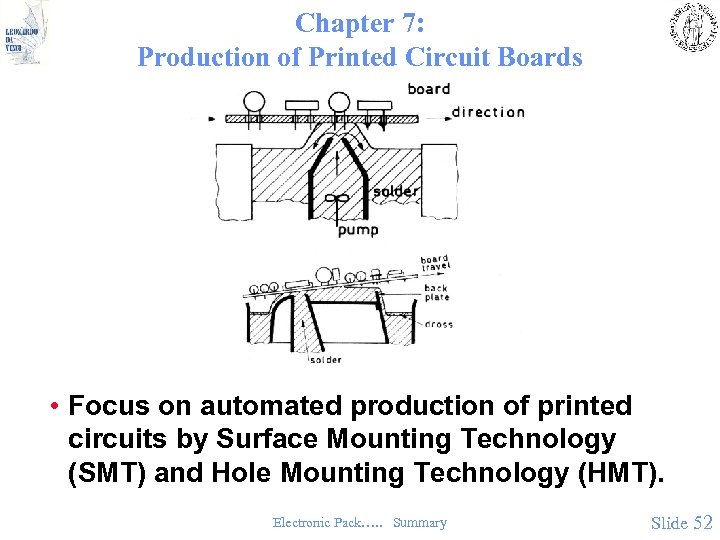 Chapter 7: Production of Printed Circuit Boards • Focus on automated production of printed circuits by Surface Mounting Technology (SMT) and Hole Mounting Technology (HMT). Electronic Pack…. . Summary Slide 52
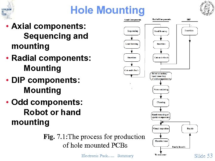 Hole Mounting • Axial components: Sequencing and mounting • Radial components: Mounting • DIP components: Mounting • Odd components: Robot or hand mounting Fig. 7. 1: The process for production of hole mounted PCBs Electronic Pack…. . Summary Slide 53
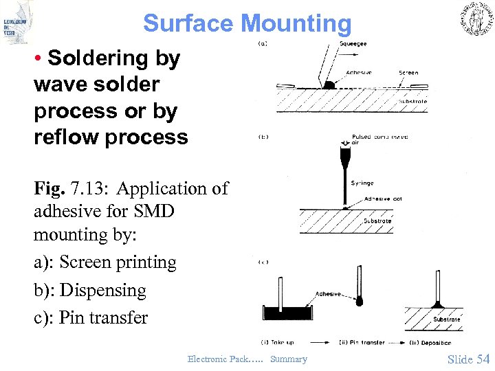 Surface Mounting • Soldering by wave solder process or by reflow process Fig. 7. 13: Application of adhesive for SMD mounting by: a): Screen printing b): Dispensing c): Pin transfer Electronic Pack…. . Summary Slide 54
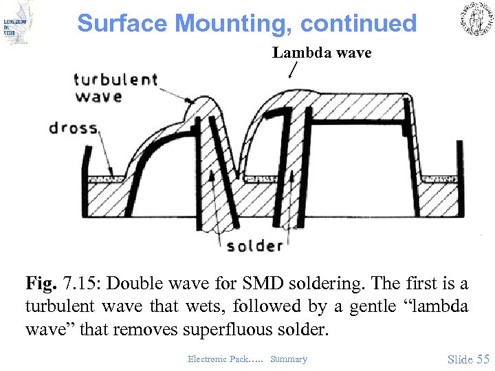 Surface Mounting, continued Lambda wave Fig. 7. 15: Double wave for SMD soldering. The first is a turbulent wave that wets, followed by a gentle “lambda wave” that removes superfluous solder. Electronic Pack…. . Summary Slide 55
 Reflow Solder Process • Print solder paste • Mount components • Dry solder paste • Solder by heating to melting of paste Electronic Pack…. . Summary Slide 56
 Other Soldering Methods • Impulse (hot bar-, thermode-) soldering • Hot plate / hot band soldering (thick film hybrid) • Hot air soldering • Laser soldering Electronic Pack…. . Summary Slide 57
 Component Placement –Automatic, dedicated pick-and-place machines –Manual placement (prototypes, repair) –Semi-manual (light guided table, etc. ) • Programmable robot • Elements of Pick-and-Place Machine – – – Board magazine/feeder system Mounting head(s) (with interchangable grip tools) Programming/control unit Component "storage" and feeder (Vision system) Electronic Pack…. . Summary Slide 58
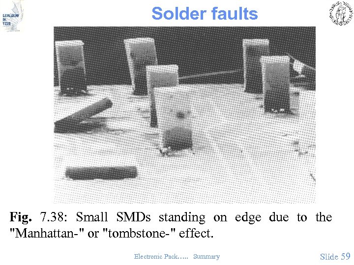 Solder faults Fig. 7. 38: Small SMDs standing on edge due to the "Manhattan-" or "tombstone-" effect. Electronic Pack…. . Summary Slide 59
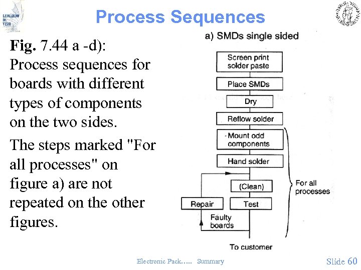 Process Sequences Fig. 7. 44 a -d): Process sequences for boards with different types of components on the two sides. The steps marked "For all processes" on figure a) are not repeated on the other figures. Electronic Pack…. . Summary Slide 60
 Board Testing • Functional test • "In-circuit" test • NB: Good designs use one-sided testing –Test jigs Electronic Pack…. . Summary Slide 61
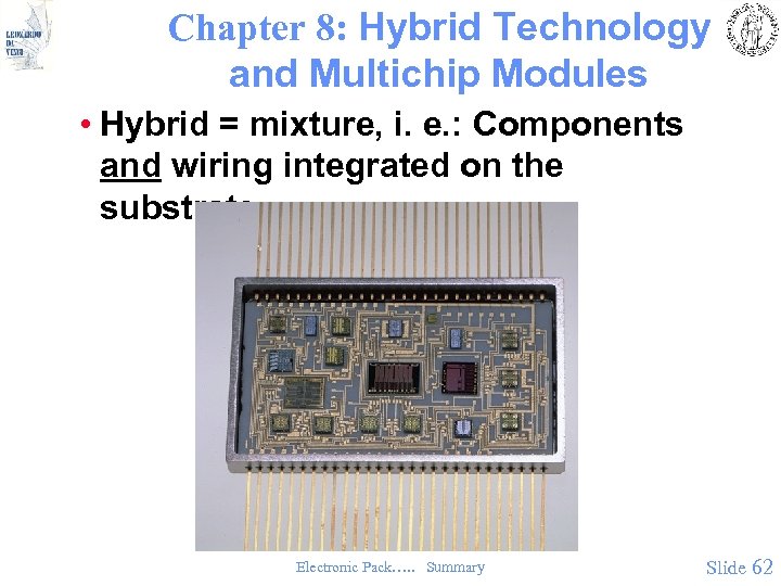 Chapter 8: Hybrid Technology and Multichip Modules • Hybrid = mixture, i. e. : Components and wiring integrated on the substrate Electronic Pack…. . Summary Slide 62
 Types of Hybrids and Multichip Modules • Thick film technology – High temperature thick film hybrid technology – Polymer thick film hybrid technology • Thin film technology – Conventional thin film technology (one conductor layer) – Multilayer thin film technology • Multichip modules: – Multilayer ceramic (MCM-C) (C for ceramic) – Multilayer thin film (MCM-D) (D for deposited) – Multilayer fineline circuit boards (MCM-L) (L for laminated) Please also confer to Chapter 5. Electronic Pack…. . Summary Slide 63
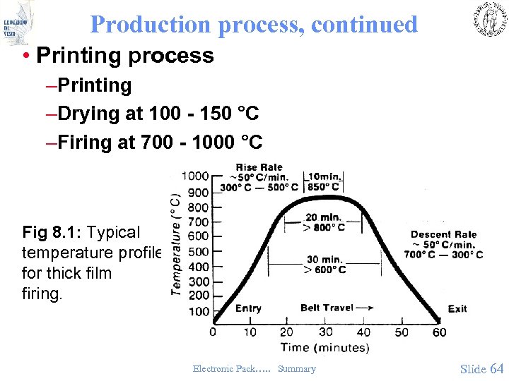 Production process, continued • Printing process –Printing –Drying at 100 - 150 °C –Firing at 700 - 1000 °C Fig 8. 1: Typical temperature profile for thick film firing. Electronic Pack…. . Summary Slide 64
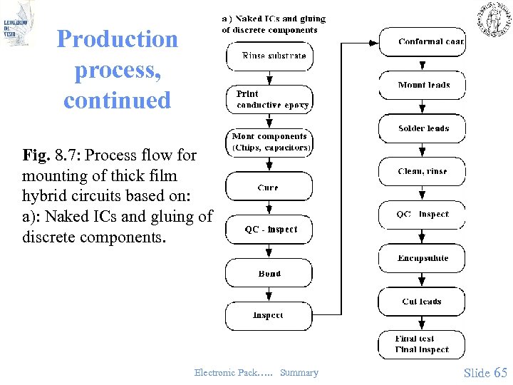 Production process, continued Fig. 8. 7: Process flow for mounting of thick film hybrid circuits based on: a): Naked ICs and gluing of discrete components. Electronic Pack…. . Summary Slide 65
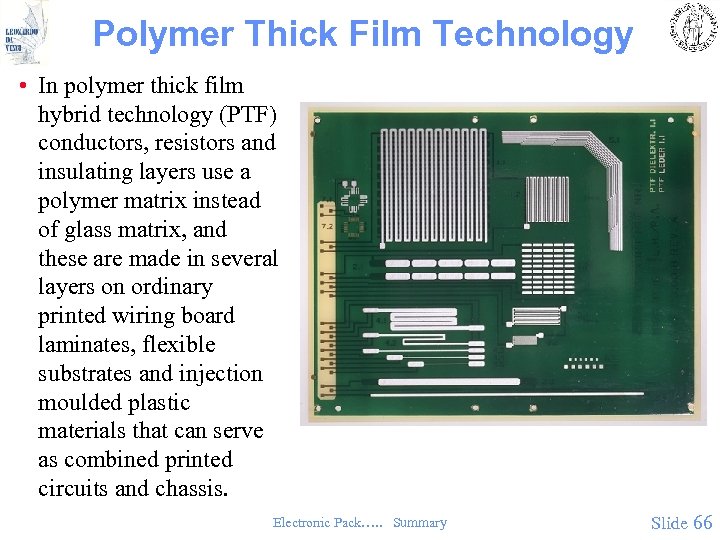 Polymer Thick Film Technology • In polymer thick film hybrid technology (PTF) conductors, resistors and insulating layers use a polymer matrix instead of glass matrix, and these are made in several layers on ordinary printed wiring board laminates, flexible substrates and injection moulded plastic materials that can serve as combined printed circuits and chassis. Electronic Pack…. . Summary Slide 66
 Thin Film Technology • Substrate materials –Alumina, glass, silicon • Conductor materials –Gold, aluminium • Resistor materials –Ni. Cr (Chromnickel), Ta 2 N (Tantalnitrid) • Insulation/dielectrics/passivation materials –Si. O 2 (Silicon dioxide), Si. N 3 (Silicon nitride), Al 2 O 3 (Silicon nitride), Ta 2 O 5 (Tantaloxide) Electronic Pack…. . Summary Slide 67
 Multilayer Thin Film - MCM-D • Process – 1. Spinning polyimide insulation – 2. Deposition Al metallization – 3. Photolithography, wet etch – 4. Spinning polyimide – 5. Etching vias – 6. Repetition steps 1 - 5 – 7. Metallization and etching of metal Electronic Pack…. . Summary Slide 68
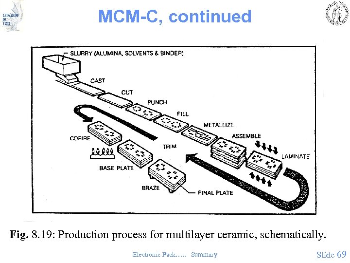 MCM-C, continued Fig. 8. 19: Production process for multilayer ceramic, schematically. Electronic Pack…. . Summary Slide 69
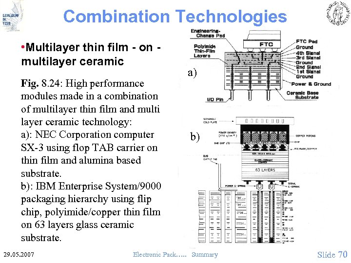 Combination Technologies • Multilayer thin film - on multilayer ceramic Fig. 8. 24: High performance modules made in a combination of multilayer thin film and multi layer ceramic technology: a): NEC Corporation computer SX-3 using flop TAB carrier on thin film and alumina based substrate. b): IBM Enterprise System/9000 packaging hierarchy using flip chip, polyimide/copper thin film on 63 layers glass ceramic substrate. 29. 05. 2007 a) b) Electronic Pack…. . Summary Slide 70
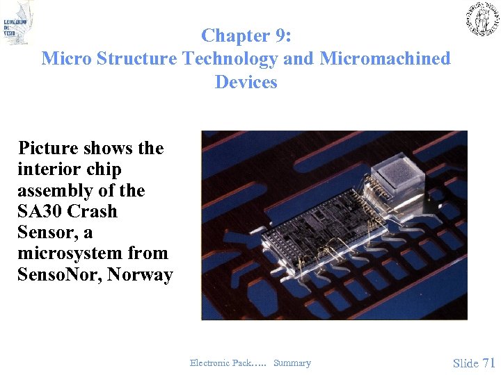 Chapter 9: Micro Structure Technology and Micromachined Devices Picture shows the interior chip assembly of the SA 30 Crash Sensor, a microsystem from Senso. Nor, Norway Electronic Pack…. . Summary Slide 71
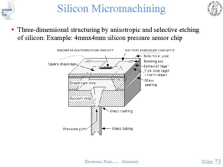 Silicon Micromachining • Three-dimensional structuring by anisotropic and selective etching of silicon: Example: 4 mmx 4 mm silicon pressure sensor chip Electronic Pack…. . Summary Slide 72
 The Top Ten Success Factors of Micromachined Devices • 1. Batch organised planar processing technology • 2. Microelectronics manufacturing infrastructure • 3. Research results from solid state technology and other related fields of microelectronics • 4. Micromachining • 5. Wafer and chip bonding • 6. Mechanical material characteristics • 7. Sensor effects • 8. Actuator functions • 9. Integrated electronics • 10. Combination of features Electronic Pack…. . Summary Slide 73
 The Bottom Ten List of Inhibiting factors • 1. Slow market acceptance • 2. Low production volumes • 3. Immature industrial infrastructure • 4. Poor reliability • 5. Complex designs and processes • 6. Immature processing technology • 7. Immature packaging and interconnection technologies • 8. Limited research resources • 9. Limited human resources • 10. High costs Electronic Pack…. . Summary Slide 74
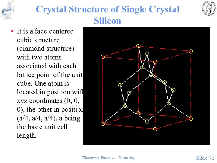 Crystal Structure of Single Crystal Silicon • It is a face-centered cubic structure (diamond structure) with two atoms associated with each lattice point of the unit cube. One atom is located in position with xyz coordinates (0, 0, 0), the other in position (a/4, a/4), a being the basic unit cell length. Electronic Pack…. . Summary Slide 75
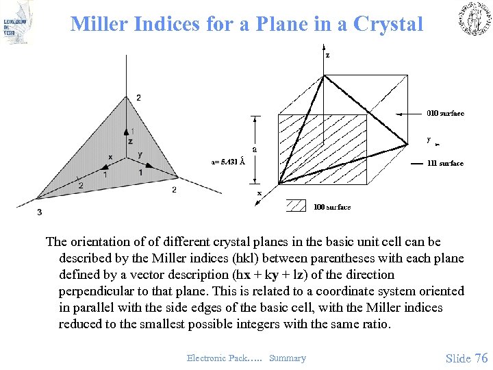 Miller Indices for a Plane in a Crystal The orientation of of different crystal planes in the basic unit cell can be described by the Miller indices (hkl) between parentheses with each plane defined by a vector description (hx + ky + lz) of the direction perpendicular to that plane. This is related to a coordinate system oriented in parallel with the side edges of the basic cell, with the Miller indices reduced to the smallest possible integers with the same ratio. Electronic Pack…. . Summary Slide 76
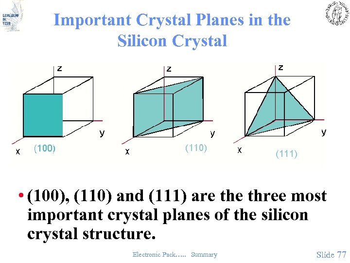 Important Crystal Planes in the Silicon Crystal • (100), (110) and (111) are three most important crystal planes of the silicon crystal structure. Electronic Pack…. . Summary Slide 77
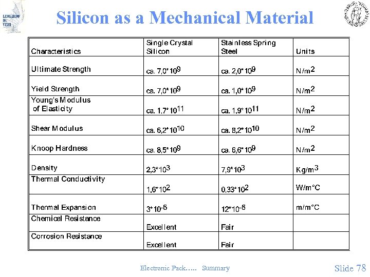 Silicon as a Mechanical Material Electronic Pack…. . Summary Slide 78
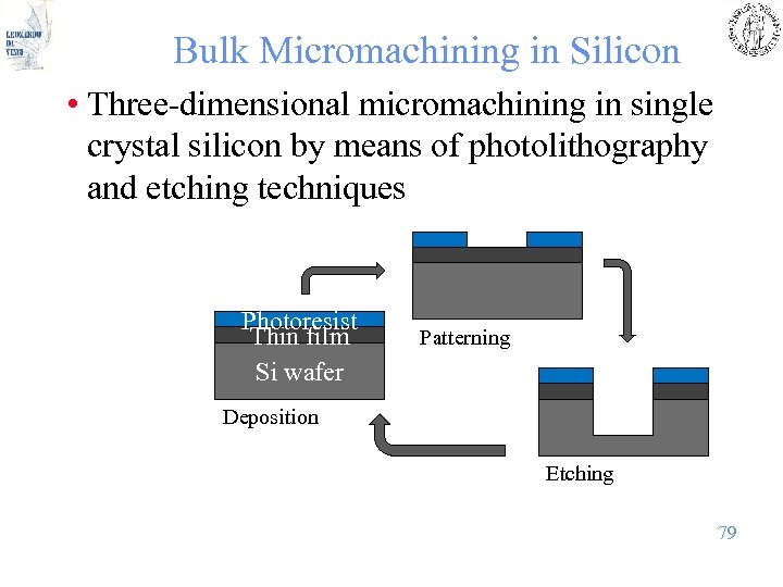 Bulk Micromachining in Silicon • Three-dimensional micromachining in single crystal silicon by means of photolithography and etching techniques Photoresist Thin film Si wafer Patterning Deposition Etching 79
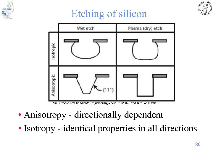 Etching of silicon An Introduction to MEMs Engineering - Nadim Maluf and Kirt Williams • Anisotropy - directionally dependent • Isotropy - identical properties in all directions 80
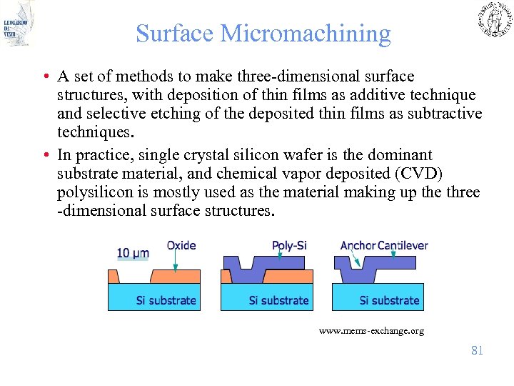 Surface Micromachining • A set of methods to make three-dimensional surface structures, with deposition of thin films as additive technique and selective etching of the deposited thin films as subtractive techniques. • In practice, single crystal silicon wafer is the dominant substrate material, and chemical vapor deposited (CVD) polysilicon is mostly used as the material making up the three -dimensional surface structures. www. mems-exchange. org 81
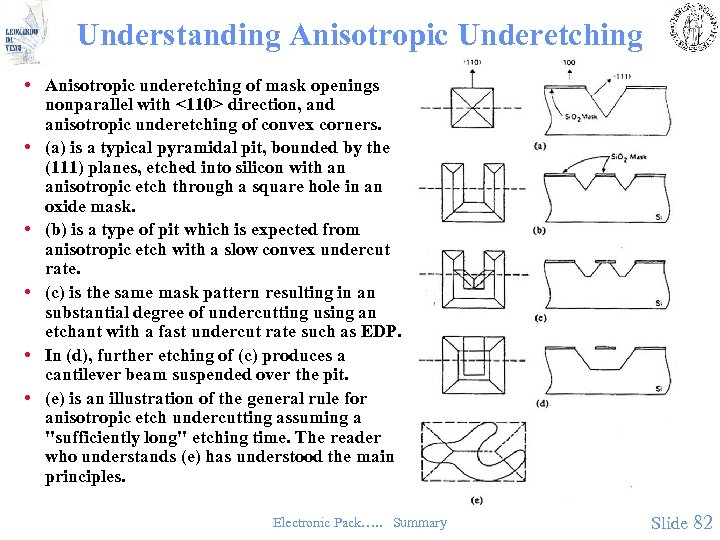 Understanding Anisotropic Underetching • Anisotropic underetching of mask openings nonparallel with <110> direction, and anisotropic underetching of convex corners. • (a) is a typical pyramidal pit, bounded by the (111) planes, etched into silicon with an anisotropic etch through a square hole in an oxide mask. • (b) is a type of pit which is expected from anisotropic etch with a slow convex undercut rate. • (c) is the same mask pattern resulting in an substantial degree of undercutting using an etchant with a fast undercut rate such as EDP. • In (d), further etching of (c) produces a cantilever beam suspended over the pit. • (e) is an illustration of the general rule for anisotropic etch undercutting assuming a "sufficiently long" etching time. The reader who understands (e) has understood the main principles. Electronic Pack…. . Summary Slide 82
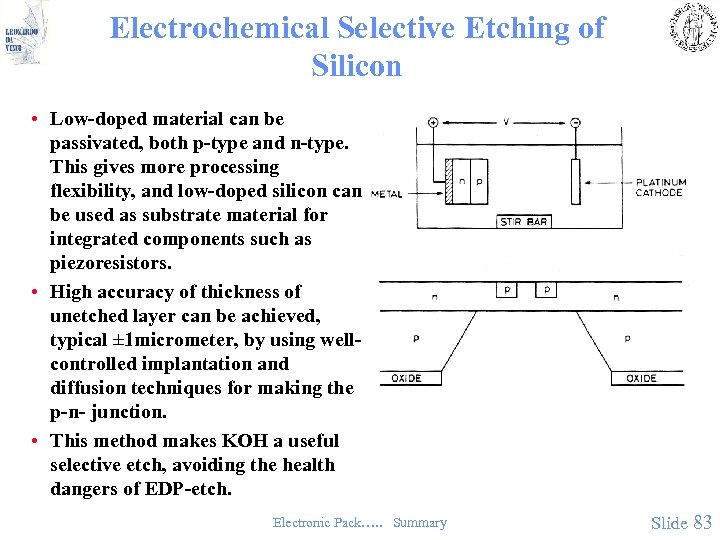 Electrochemical Selective Etching of Silicon • Low-doped material can be passivated, both p-type and n-type. This gives more processing flexibility, and low-doped silicon can be used as substrate material for integrated components such as piezoresistors. • High accuracy of thickness of unetched layer can be achieved, typical ± 1 micrometer, by using wellcontrolled implantation and diffusion techniques for making the p-n- junction. • This method makes KOH a useful selective etch, avoiding the health dangers of EDP-etch. Electronic Pack…. . Summary Slide 83
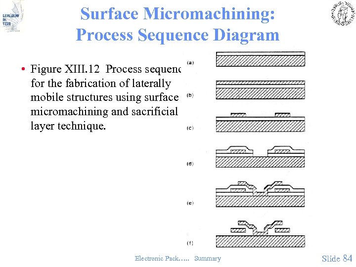 Surface Micromachining: Process Sequence Diagram • Figure XIII. 12 Process sequence for the fabrication of laterally mobile structures using surface micromachining and sacrificial layer technique. Electronic Pack…. . Summary Slide 84
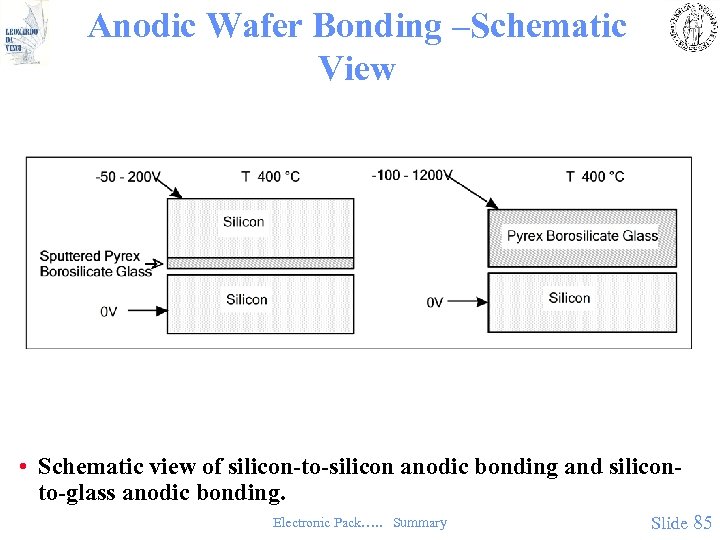 Anodic Wafer Bonding –Schematic View • Schematic view of silicon-to-silicon anodic bonding and siliconto-glass anodic bonding. Electronic Pack…. . Summary Slide 85
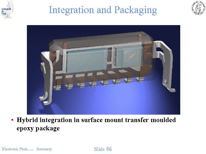 Integration and Packaging • Hybrid integration in surface mount transfer moulded epoxy package Electronic Pack…. . Summary Slide 86
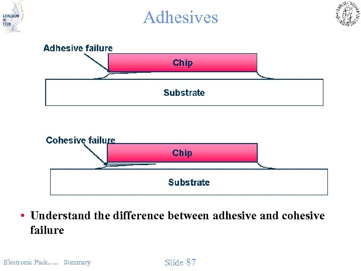 Adhesives • Understand the difference between adhesive and cohesive failure Electronic Pack…. . Summary Slide 87
 Adhesives • Thermoset adhesives – Do not melt upon heating – Forms links or chemical bonds between adjacent chains, during curing (intra-molecular bonds) – Three dimensional rigid network – Properties depend on the molecular units, and the length and the density of the cross-links – Thermosetting resins are usually isotropic – Mostly epoxies, silicones, urethanes Electronic Pack…. . Summary Slide 88
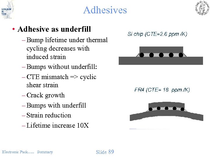 Adhesives • Adhesive as underfill – Bump lifetime under thermal cycling decreases with induced strain – Bumps without underfill: – CTE mismatch => cyclic shear strain – Crack growth – Bumps with underfill – Strain reduction – Lifetime increase 10 X Electronic Pack…. . Summary Slide 89
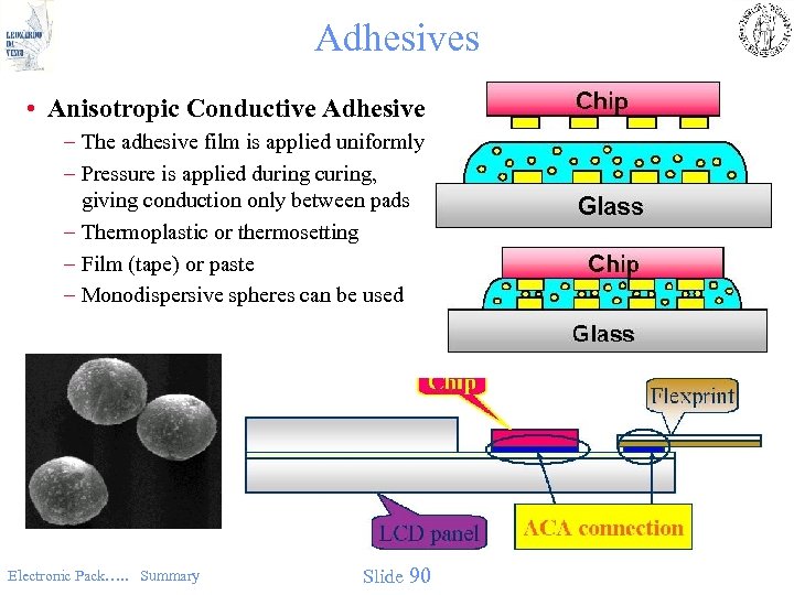 Adhesives • Anisotropic Conductive Adhesive – The adhesive film is applied uniformly – Pressure is applied during curing, giving conduction only between pads – Thermoplastic or thermosetting – Film (tape) or paste – Monodispersive spheres can be used Electronic Pack…. . Summary Slide 90
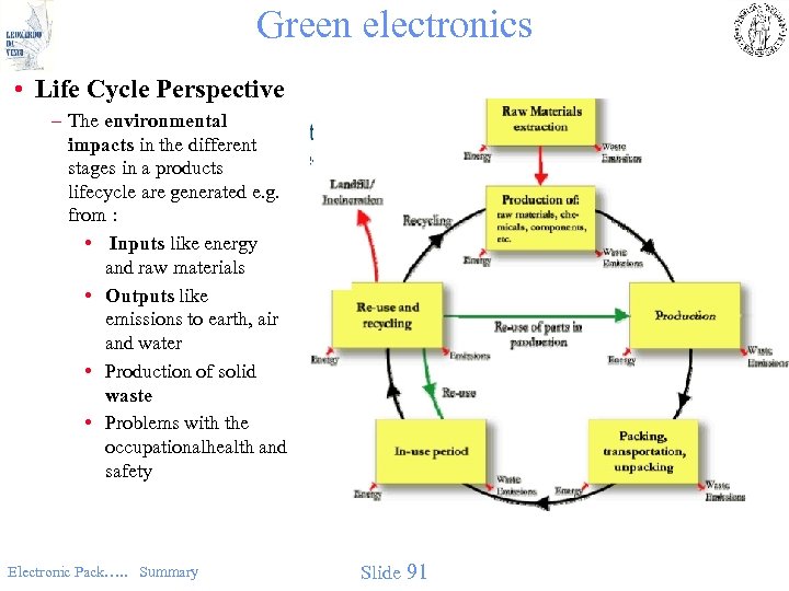 Green electronics • Life Cycle Perspective – The environmental impacts in the different stages in a products lifecycle are generated e. g. from : • Inputs like energy and raw materials • Outputs like emissions to earth, air and water • Production of solid waste • Problems with the occupationalhealth and safety Electronic Pack…. . Summary Slide 91
 Ro. HS – in brief • The Ro. HS Regulations ban the placing on the EU market of new Electrical and Electronic Equipment (EEE) containing more than the set levels of lead, cadmium, mercury, hexavalent chromium and both polybrominated biphenyl (PBB) and polybrominated diphenyl ether (PBDE) flame retardants from 1 July 2006. There a number of exempted applications for these substances. • Manufacturers will need to ensure that their products - and the components of such products - comply with the requirements of the Regulations by the relevant date in order to be placed on the Single Market. The Regulations will also have an impact on those who import EEE into the European Union on a professional basis, those who export to other Member States and those who rebrand other manufacturers’ EEE as their own. • These Regulations do not affect the application of existing legal requirements for EEE, including those regarding safety, the protection of health, existing transport requirements or provisions on hazardous waste. In other words, existing legislation on EEE and hazardous substances must also be complied with. Electronic Pack…. . Summary Slide 92
 Legislation • EEE has the authorities' attention, primarily because of the rising amounts of waste and the connected disposal problems. • This is the reason why since the beginning of the nineties there has been an ongoing work on legislation in this field, starting in Germany, Denmark, The Netherlands, Sweden and Norway, as well as on the EU-scale. • The regulations are primarily concerned with: – establishing collection systems and securing correct handling of waste, which means recycling and regaining of resources – safe separation and disposal of environmental hazardous parts – certain hazardous substances, which will either be banned or restricted in use • The regulations also introduces a producer responsibility for the disposal, and demands information from the producer to the recycler about e. g. the content of environmentally hazardous parts and possibilities for recycling. Electronic Pack…. . Summary Slide 93
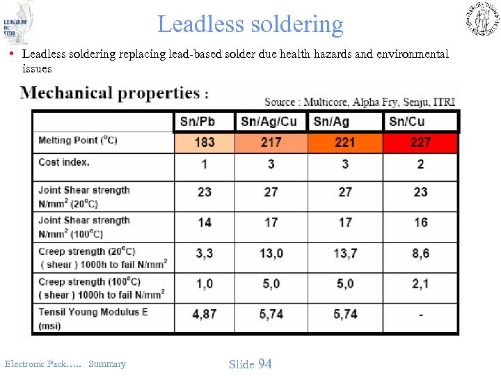 Leadless soldering • Leadless soldering replacing lead-based solder due health hazards and environmental issues Electronic Pack…. . Summary Slide 94
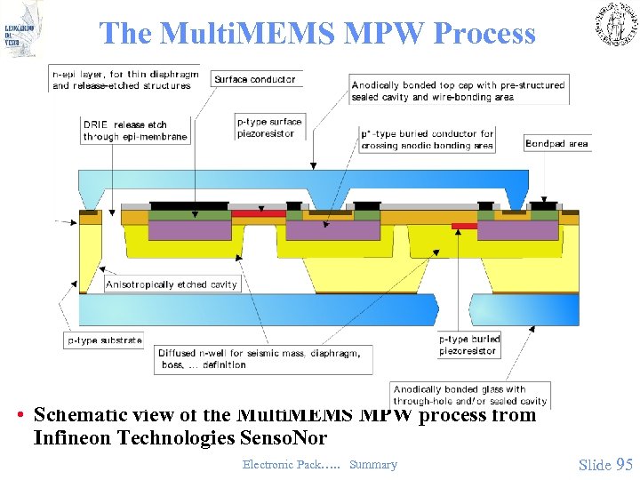 The Multi. MEMS MPW Process • Schematic view of the Multi. MEMS MPW process from Infineon Technologies Senso. Nor Electronic Pack…. . Summary Slide 95
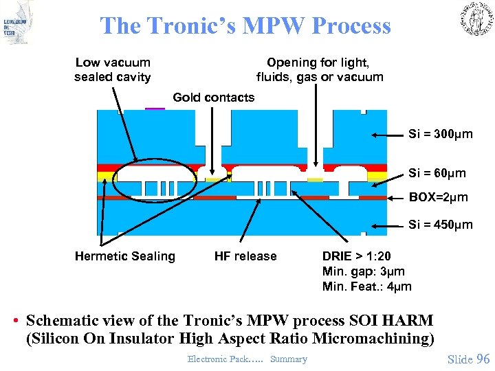 The Tronic’s MPW Process Low vacuum sealed cavity Opening for light, fluids, gas or vacuum Gold contacts Si = 300µm Si = 60µm BOX=2µm Si = 450µm Hermetic Sealing HF release DRIE > 1: 20 Min. gap: 3µm Min. Feat. : 4µm • Schematic view of the Tronic’s MPW process SOI HARM (Silicon On Insulator High Aspect Ratio Micromachining) Electronic Pack…. . Summary Slide 96
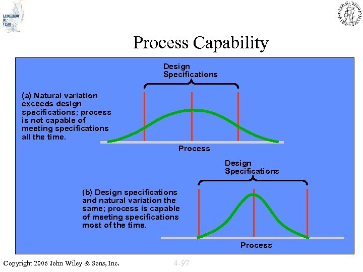 Process Capability Design Specifications (a) Natural variation exceeds design specifications; process is not capable of meeting specifications all the time. Process Design Specifications (b) Design specifications and natural variation the same; process is capable of meeting specifications most of the time. Process Copyright 2006 John Wiley & Sons, Inc. 4 -97
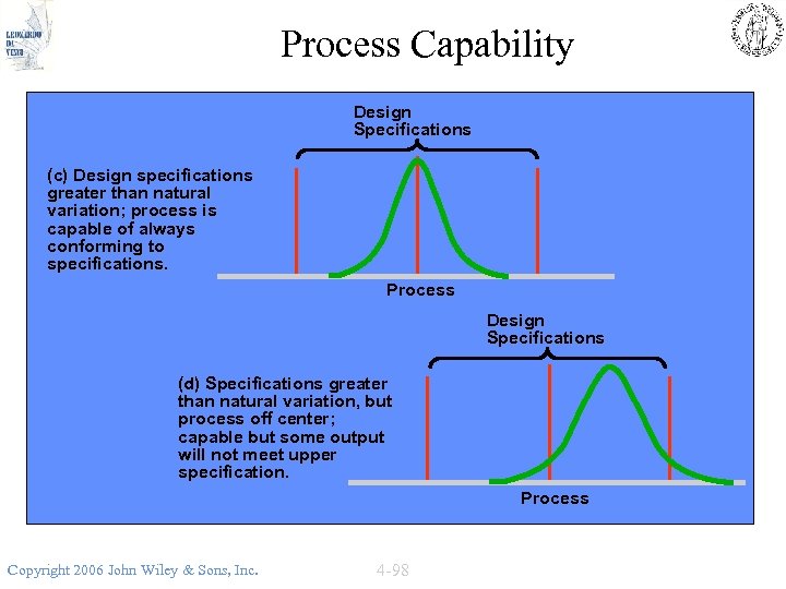 Process Capability Design Specifications (c) Design specifications greater than natural variation; process is capable of always conforming to specifications. Process Design Specifications (d) Specifications greater than natural variation, but process off center; capable but some output will not meet upper specification. Process Copyright 2006 John Wiley & Sons, Inc. 4 -98
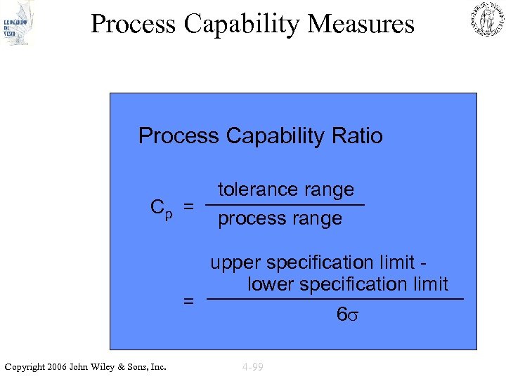 Process Capability Measures Process Capability Ratio Cp = = Copyright 2006 John Wiley & Sons, Inc. tolerance range process range upper specification limit lower specification limit 6 4 -99
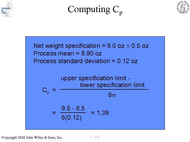 Computing Cp Net weight specification = 9. 0 oz 0. 5 oz Process mean = 8. 80 oz Process standard deviation = 0. 12 oz Cp = upper specification limit lower specification limit 6 9. 5 - 8. 5 = = 1. 39 6(0. 12) Copyright 2006 John Wiley & Sons, Inc. 4 -100
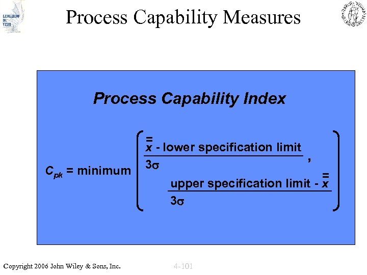 Process Capability Measures Process Capability Index Cpk = minimum Copyright 2006 John Wiley & Sons, Inc. = x - lower specification limit , 3 = upper specification limit - x 3 4 -101
 Copyright 2006 John Wiley & Sons, Inc. 4 -102
 Electronic Pack…. . Summary Slide 103
 Copyright 2006 John Wiley & Sons, Inc. 4 -104
 End of Summary • Use this summary lecture as a guideline to what is considered the most important parts of the course syllabus. • Look at earlier exam tests and guides to get a feeling of the kind of questions that will be asked. • Get the basic overview, and know the differences between the different technologies ( «Getting a C grade» ) – For instance, do not wrongly describe the process technology asked for by intermixing it with another technology – for instance know the differences between thick film technology and thin film technology. • Then, start to learn and understand the finer details to be able to show you have a deep knowledge of the syllabus ( «Going for the A grade» ) • An understanding of work done in the Compulsory Project is expected, and highly probable a part of the Final Exam! (Active group membership will be hounoured – passivity punished) • Good luck with your Examination Test, and thank you for attending this course! Electronic Pack…. . Summary Slide 105


