f5d55903345344a9b428599c053e7068.ppt
- Количество слайдов: 20
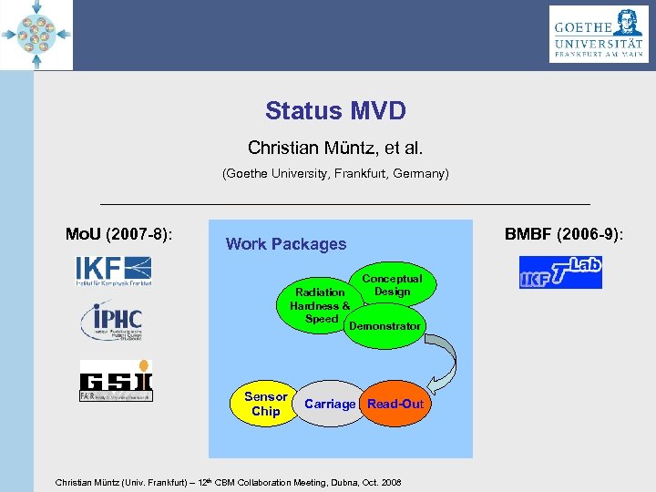 Status MVD Christian Müntz, et al. (Goethe University, Frankfurt, Germany) Mo. U (2007 -8): BMBF (2006 -9): Work Packages Conceptual Design Radiation Hardness & Speed Demonstrator Sensor Chip Carriage Read-Out Christian Müntz (Univ. Frankfurt) – 12 th CBM Collaboration Meeting, Dubna, Oct. 2008
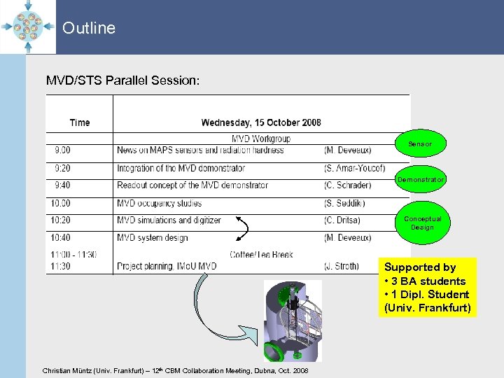 Outline MVD/STS Parallel Session: Sensor Demonstrator Conceptual Design Supported by • 3 BA students • 1 Dipl. Student (Univ. Frankfurt) Christian Müntz (Univ. Frankfurt) – 12 th CBM Collaboration Meeting, Dubna, Oct. 2008
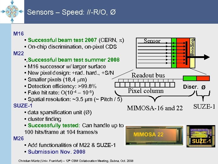 M 16 • Successful beam test 2007 (CERN, p) • On-chip discrimination, on-pixel CDS M 22 Sensor Bonding. Sensors – Speed: //-R/O, Ø • , Successful beam test summer 2008 • M 16 successor w/ larger surface • New pixel design: +rad. hard. , +S/N Readout bus • Smaller pixels (18, 4 mm) • Detection efficiency: >99. 8% Discr. Ø Pixel column • Fake hit rate: O(10 -4 – 10 -5) • Spatial resolution: ~3. 5 µm (~ Pitch / 5) SUZE-1 MIMOSA-16 and 22 • data sparsification unit (Ø) • cluster finding • Successfully tested: Can handle up to 100 hits/frame at 104 frames/s MIMOSA 22 M 26 SUZE-1 • Add functionalities of M 22 & SUZE-1 • Submission Nov. 2008 Christian Müntz (Univ. Frankfurt) – 12 th CBM Collaboration Meeting, Dubna, Oct. 2008
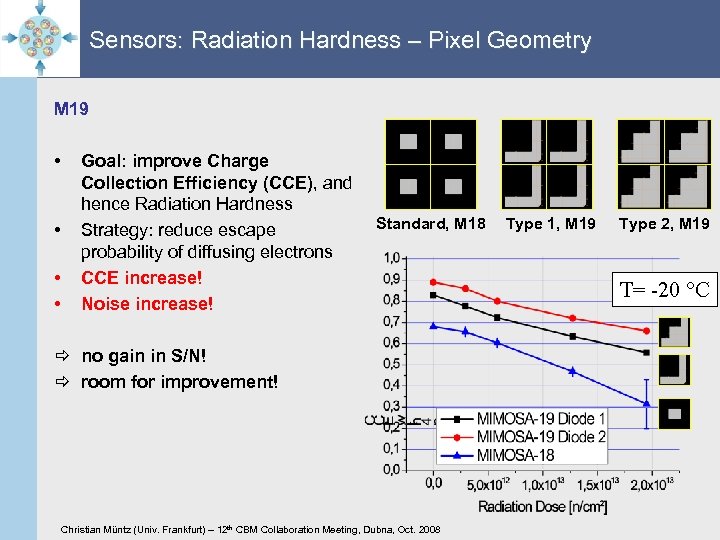 Sensors: Radiation Hardness – Pixel Geometry M 19 • • Goal: improve Charge Collection Efficiency (CCE), and hence Radiation Hardness Strategy: reduce escape probability of diffusing electrons CCE increase! Noise increase! Standard, M 18 no gain in S/N! room for improvement! Christian Müntz (Univ. Frankfurt) – 12 th CBM Collaboration Meeting, Dubna, Oct. 2008 Type 1, M 19 Type 2, M 19 T= -20 °C
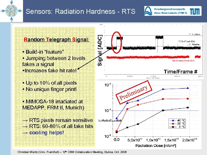 Random Telegraph Signal: • Build-in “feature” • Jumping between 2 levels fakes a signal • Increases fake hit rate! Signal [ADC] Sensors: Radiation Hardness - RTS Time/Frame # • Up to 10% of all pixels • No unique finger print! • MIMOSA-18 irradiated at MEDAPP, FRM II, Munich) y Pre l → RTS pixels remain sensitive → RTS: 60 -80% of all fake hits → cooling helps! Christian Müntz (Univ. Frankfurt) – 12 th CBM Collaboration Meeting, Dubna, Oct. 2008 inar im
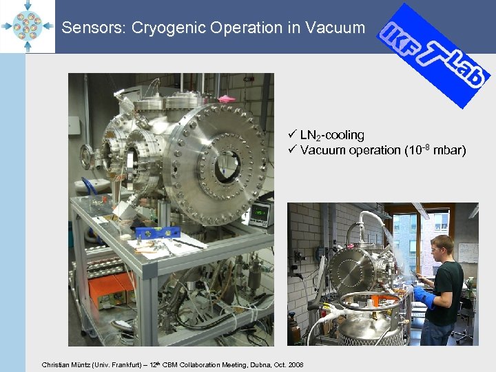 Sensors: Cryogenic Operation in Vacuum ü LN 2 -cooling ü Vacuum operation (10 -8 mbar) Christian Müntz (Univ. Frankfurt) – 12 th CBM Collaboration Meeting, Dubna, Oct. 2008
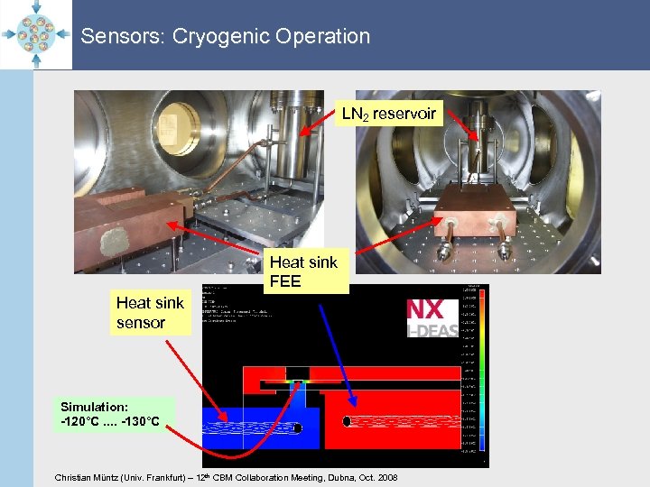 Sensors: Cryogenic Operation LN 2 reservoir Heat sink FEE Heat sink sensor Simulation: -120°C. . -130°C Christian Müntz (Univ. Frankfurt) – 12 th CBM Collaboration Meeting, Dubna, Oct. 2008
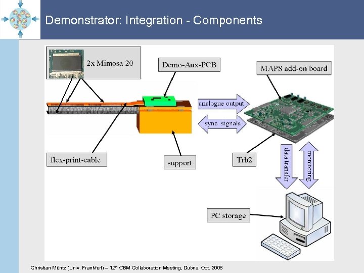 Demonstrator: Integration - Components Christian Müntz (Univ. Frankfurt) – 12 th CBM Collaboration Meeting, Dubna, Oct. 2008
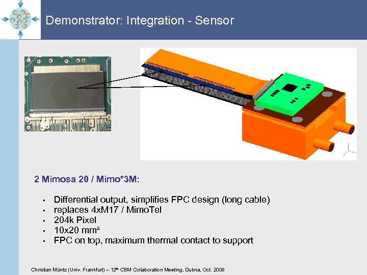 Demonstrator: Integration - Sensor 2 Mimosa 20 / Mimo*3 M: • • • Differential output, simplifies FPC design (long cable) replaces 4 x. M 17 / Mimo. Tel 204 k Pixel 10 x 20 mm² FPC on top, maximum thermal contact to support Christian Müntz (Univ. Frankfurt) – 12 th CBM Collaboration Meeting, Dubna, Oct. 2008
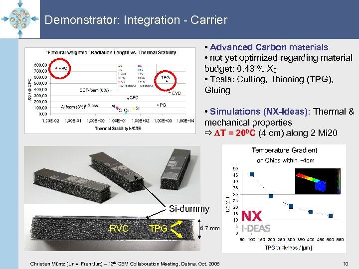 Demonstrator: Integration - Carrier • Advanced Carbon materials • not yet optimized regarding material budget: 0. 43 % X 0 • Tests: Cutting, thinning (TPG), Gluing • Simulations (NX-Ideas): Thermal & mechanical properties DT = 200 C (4 cm) along 2 Mi 20 Si-dummy RVC TPG 6. 7 mm Christian Müntz (Univ. Frankfurt) – 12 th CBM Collaboration Meeting, Dubna, Oct. 2008 10
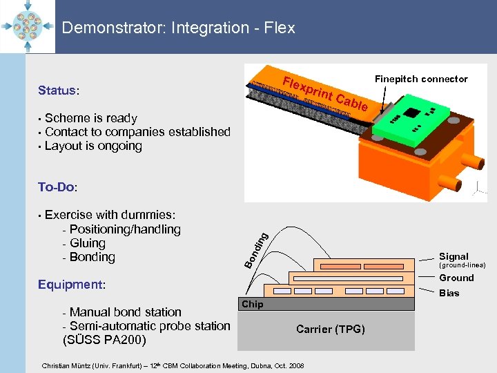 Demonstrator: Integration - Flex Status: Scheme is ready • Contact to companies established • Layout is ongoing prin Finepitch connector t Ca ble • nd Exercise with dummies: - Positioning/handling - Gluing - Bonding Signal Bo • ing To-Do: (ground-lines) Ground Equipment: Manual bond station - Semi-automatic probe station (SÜSS PA 200) - Bias Chip Carrier (TPG) Christian Müntz (Univ. Frankfurt) – 12 th CBM Collaboration Meeting, Dubna, Oct. 2008
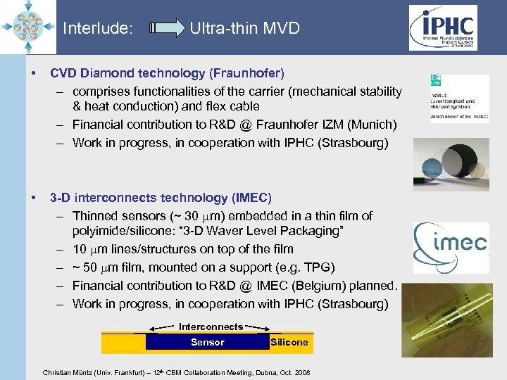 Interlude: Ultra-thin MVD • CVD Diamond technology (Fraunhofer) – comprises functionalities of the carrier (mechanical stability & heat conduction) and flex cable – Financial contribution to R&D @ Fraunhofer IZM (Munich) – Work in progress, in cooperation with IPHC (Strasbourg) • 3 -D interconnects technology (IMEC) – Thinned sensors (~ 30 mm) embedded in a thin film of polyimide/silicone: “ 3 -D Waver Level Packaging” – 10 mm lines/structures on top of the film – ~ 50 mm film, mounted on a support (e. g. TPG) – Financial contribution to R&D @ IMEC (Belgium) planned. – Work in progress, in cooperation with IPHC (Strasbourg) Interconnects Sensor Silicone Christian Müntz (Univ. Frankfurt) – 12 th CBM Collaboration Meeting, Dubna, Oct. 2008
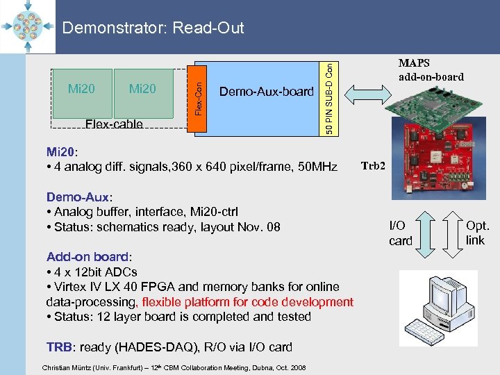 Mi 20 Demo-Aux-board Flex-cable Mi 20: • 4 analog diff. signals, 360 x 640 pixel/frame, 50 MHz Demo-Aux: • Analog buffer, interface, Mi 20 -ctrl • Status: schematics ready, layout Nov. 08 Add-on board: • 4 x 12 bit ADCs • Virtex IV LX 40 FPGA and memory banks for online data-processing, flexible platform for code development • Status: 12 layer board is completed and tested TRB: ready (HADES-DAQ), R/O via I/O card Christian Müntz (Univ. Frankfurt) – 12 th CBM Collaboration Meeting, Dubna, Oct. 2008 MAPS add-on-board 50 PIN SUB-D Con Mi 20 Flex-Con Demonstrator: Read-Out Trb 2 I/O card Opt. link
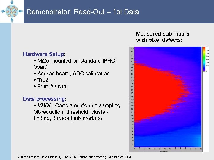 Demonstrator: Read-Out – 1 st Data Measured sub matrix with pixel defects: Hardware Setup: • Mi 20 mounted on standard IPHC board • Add-on board, ADC calibration • Trb 2 • Fast I/O card Data processing: • VHDL: Correlated double sampling, bit-reduction, threshold, clusterfinding, data-output-interface Christian Müntz (Univ. Frankfurt) – 12 th CBM Collaboration Meeting, Dubna, Oct. 2008
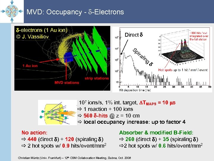 MVD: Occupancy - d-Electrons d-electrons (1 Au ion) © J. Vassiliev Direct d Sp i ra lin g d 107 ions/s, 1% int. target, DTMAPS = 10 ms 1 reaction + 100 ions 560 d-hits @ z = 10 cm local occupancy increase: up to factor 4 No action: 440 (direct d) + 120 (spiraling d) 2 hot spots w/ 0. 9 hits/event/mm 2 Absorber & modified B-Field: 260 (direct d) + 35 (spiraling d) 2 hot spots w/ 0. 6 hits/event/mm 2 Christian Müntz (Univ. Frankfurt) – 12 th CBM Collaboration Meeting, Dubna, Oct. 2008
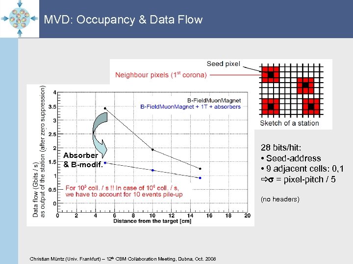 MVD: Occupancy & Data Flow Absorber & B-modif. 28 bits/hit: • Seed-address • 9 adjacent cells: 0, 1 s = pixel-pitch / 5 (no headers) Christian Müntz (Univ. Frankfurt) – 12 th CBM Collaboration Meeting, Dubna, Oct. 2008
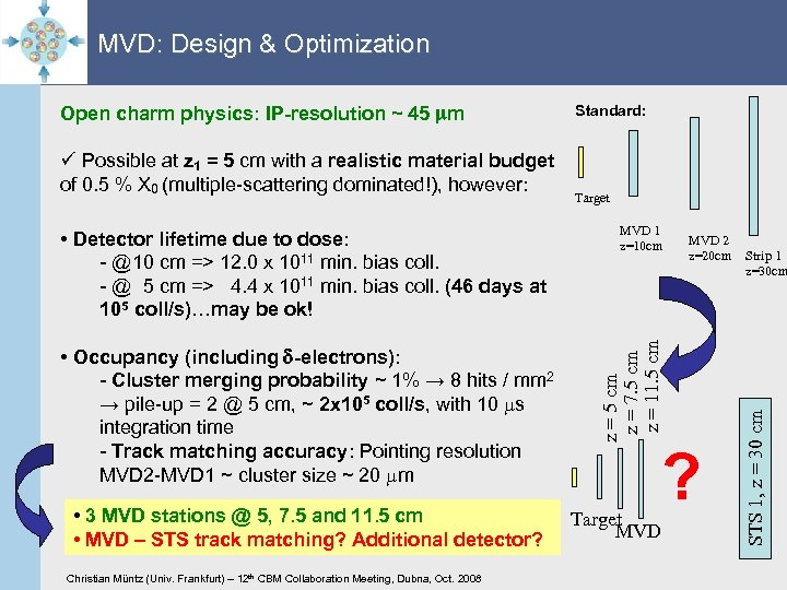 MVD: Design & Optimization • Detector lifetime due to dose: - @10 cm => 12. 0 x 1011 min. bias coll. - @ 5 cm => 4. 4 x 10¹¹ min. bias coll. (46 days at 105 coll/s)…may be ok! • Occupancy (including d-electrons): - Cluster merging probability ~ 1% → 8 hits / mm 2 → pile-up = 2 @ 5 cm, ~ 2 x 10⁵ coll/s, with 10 ms integration time - Track matching accuracy: Pointing resolution MVD 2 -MVD 1 ~ cluster size ~ 20 mm • 3 MVD stations @ 5, 7. 5 and 11. 5 cm • MVD – STS track matching? Additional detector? Christian Müntz (Univ. Frankfurt) – 12 th CBM Collaboration Meeting, Dubna, Oct. 2008 Target MVD 1 z=10 cm MVD 2 z=20 cm ? Target MVD Strip 1 z=30 cm STS 1, z = 30 cm ü Possible at z 1 = 5 cm with a realistic material budget of 0. 5 % X 0 (multiple-scattering dominated!), however: Standard: z = 5 cm z = 7. 5 cm z = 11. 5 cm Open charm physics: IP-resolution ~ 45 mm
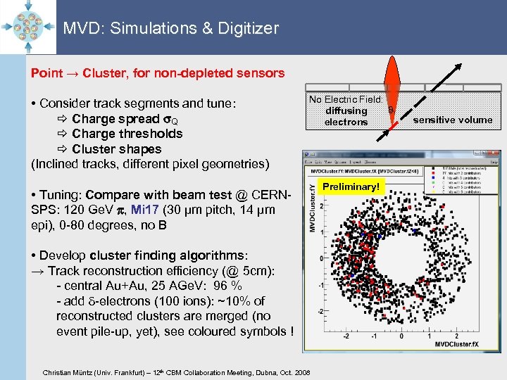 MVD: Simulations & Digitizer Point → Cluster, for non-depleted sensors • Consider track segments and tune: Charge spread s. Q Charge thresholds Cluster shapes (Inclined tracks, different pixel geometries) No Electric Field: θ diffusing electrons • Tuning: Compare with beam test @ CERNSPS: 120 Ge. V p, Mi 17 (30 μm pitch, 14 μm epi), 0 -80 degrees, no B • Develop cluster finding algorithms: → Track reconstruction efficiency (@ 5 cm): - central Au+Au, 25 AGe. V: 96 % - add d-electrons (100 ions): ~10% of reconstructed clusters are merged (no event pile-up, yet), see coloured symbols ! Christian Müntz (Univ. Frankfurt) – 12 th CBM Collaboration Meeting, Dubna, Oct. 2008 Preliminary! sensitive volume
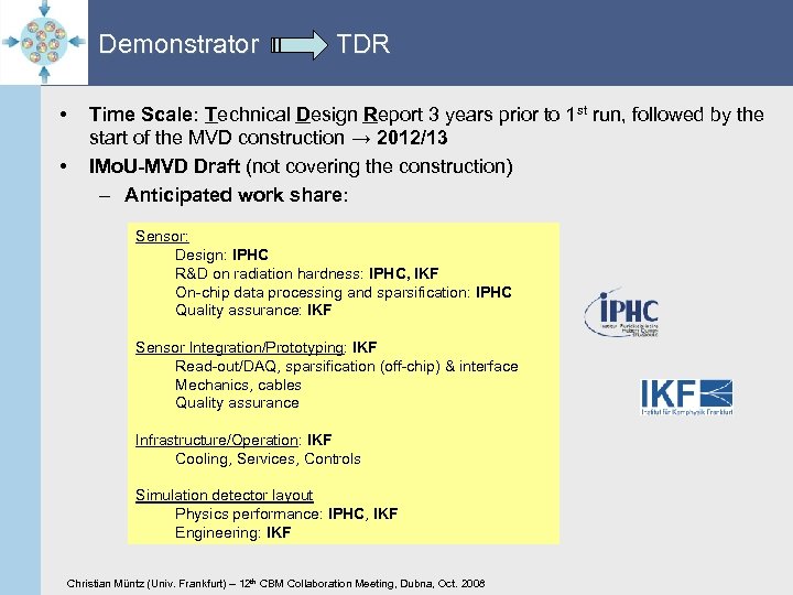 Demonstrator • • TDR Time Scale: Technical Design Report 3 years prior to 1 st run, followed by the start of the MVD construction → 2012/13 IMo. U-MVD Draft (not covering the construction) – Anticipated work share: Sensor: Design: IPHC R&D on radiation hardness: IPHC, IKF On-chip data processing and sparsification: IPHC Quality assurance: IKF Sensor Integration/Prototyping: IKF Read-out/DAQ, sparsification (off-chip) & interface Mechanics, cables Quality assurance Infrastructure/Operation: IKF Cooling, Services, Controls Simulation detector layout Physics performance: IPHC, IKF Engineering: IKF Christian Müntz (Univ. Frankfurt) – 12 th CBM Collaboration Meeting, Dubna, Oct. 2008
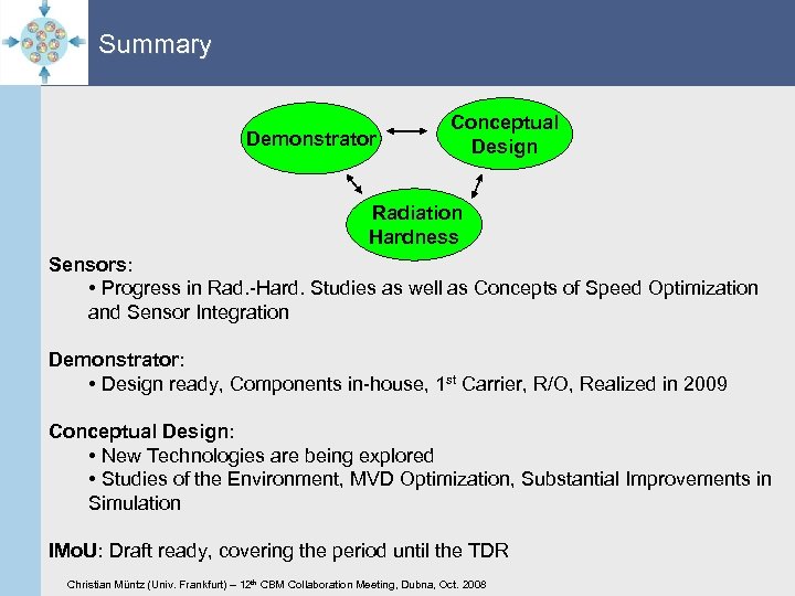 Summary Demonstrator Conceptual Design Radiation Hardness Sensors: • Progress in Rad. -Hard. Studies as well as Concepts of Speed Optimization and Sensor Integration Demonstrator: • Design ready, Components in-house, 1 st Carrier, R/O, Realized in 2009 Conceptual Design: • New Technologies are being explored • Studies of the Environment, MVD Optimization, Substantial Improvements in Simulation IMo. U: Draft ready, covering the period until the TDR Christian Müntz (Univ. Frankfurt) – 12 th CBM Collaboration Meeting, Dubna, Oct. 2008


