73e360303a54e858a9ee7e62b3035d2e.ppt
- Количество слайдов: 40
 Solid State Devices EE 3311 SMU Chapter 2 Lithography
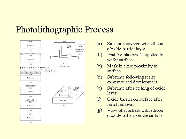 Photolithographic Process (a) (b) (c) (d) (e) (f) (g) Substrate covered with silicon dioxide barrier layer Positive photoresist applied to wafer surface Mask in close proximity to surface Substrate following resist exposure and development Substrate after etching of oxide layer Oxide barrier on surface after resist removal View of substrate with silicon dioxide pattern on the surface
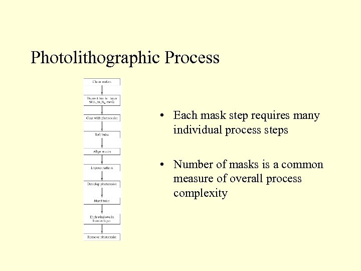 Photolithographic Process • Each mask step requires many individual process steps • Number of masks is a common measure of overall process complexity
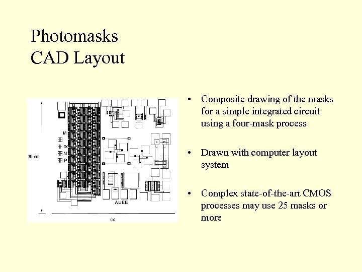 Photomasks CAD Layout • Composite drawing of the masks for a simple integrated circuit using a four-mask process • Drawn with computer layout system • Complex state-of-the-art CMOS processes may use 25 masks or more
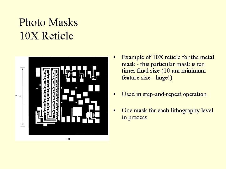 Photo Masks 10 X Reticle • Example of 10 X reticle for the metal mask - this particular mask is ten times final size (10 mm minimum feature size - huge!) • Used in step-and-repeat operation • One mask for each lithography level in process
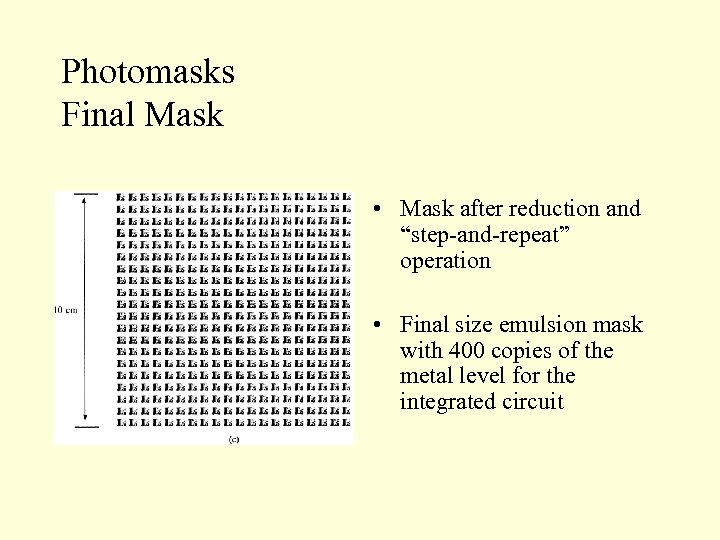 Photomasks Final Mask • Mask after reduction and “step-and-repeat” operation • Final size emulsion mask with 400 copies of the metal level for the integrated circuit
 ITRS Lithography Projections
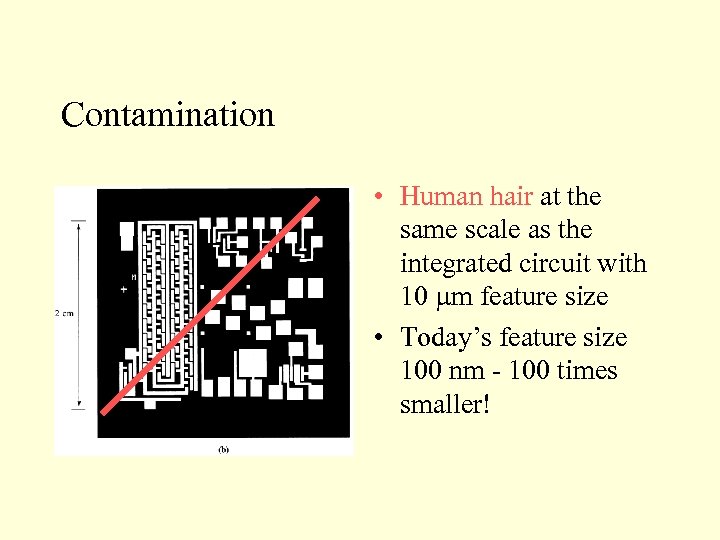 Contamination • Human hair at the same scale as the integrated circuit with 10 mm feature size • Today’s feature size 100 nm - 100 times smaller!
 Clean Room Specifications
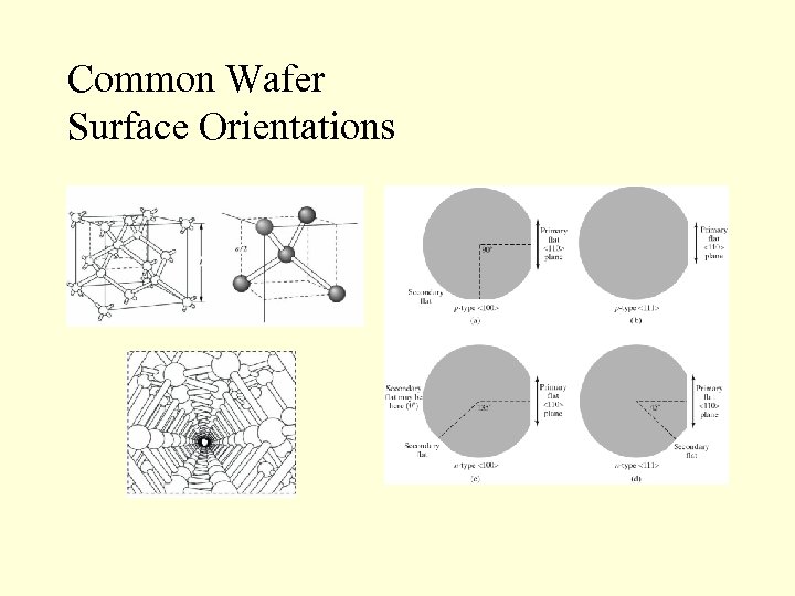 Common Wafer Surface Orientations
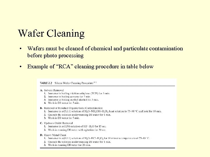 Wafer Cleaning • Wafers must be cleaned of chemical and particulate contamination before photo processing • Example of “RCA” cleaning procedure in table below
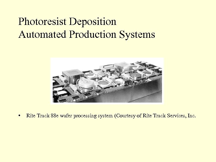 Photoresist Deposition Automated Production Systems • Rite Track 88 e wafer processing system (Courtesy of Rite Track Services, Inc.
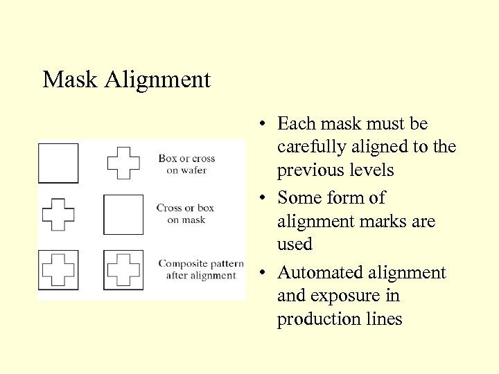 Mask Alignment • Each mask must be carefully aligned to the previous levels • Some form of alignment marks are used • Automated alignment and exposure in production lines
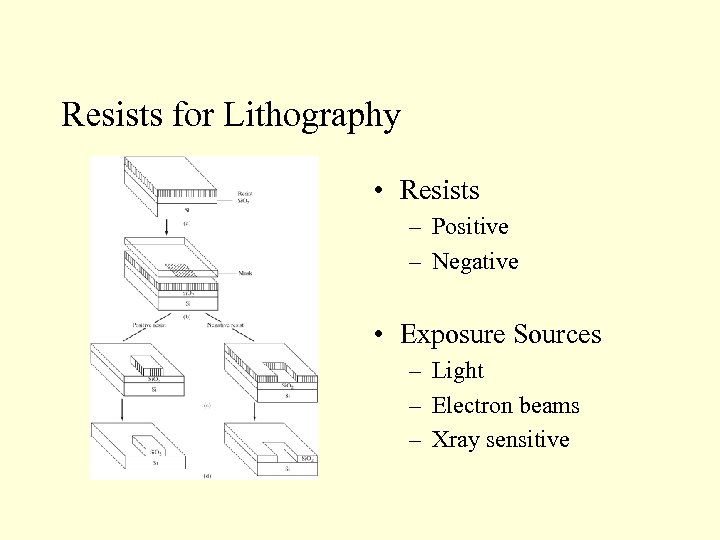 Resists for Lithography • Resists – Positive – Negative • Exposure Sources – Light – Electron beams – Xray sensitive
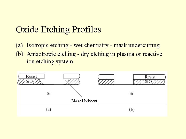 Oxide Etching Profiles (a) Isotropic etching - wet chemistry - mask undercutting (b) Anisotropic etching - dry etching in plasma or reactive ion etching system Mask Undercut
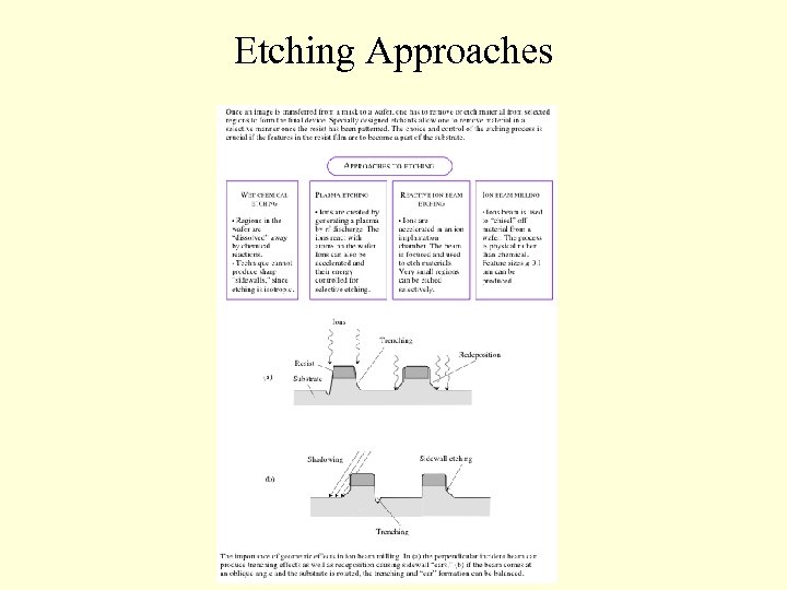 Etching Approaches
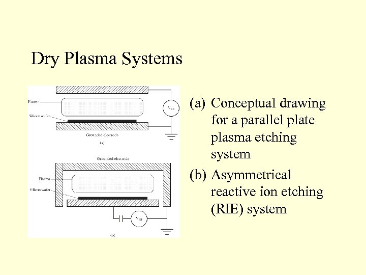 Dry Plasma Systems (a) Conceptual drawing for a parallel plate plasma etching system (b) Asymmetrical reactive ion etching (RIE) system
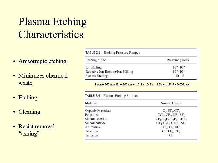 Plasma Etching Characteristics • Anisotropic etching • Minimizes chemical waste • Etching • Cleaning • Resist removal “ashing” 1 atm = 760 mm Hg = 760 torr = 1. 013 x 105 Pa 1 Pa = 1 N/m 2 = 0. 0075 torr
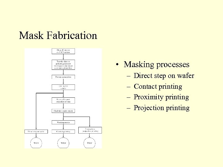 Mask Fabrication • Masking processes – – Direct step on wafer Contact printing Proximity printing Projection printing
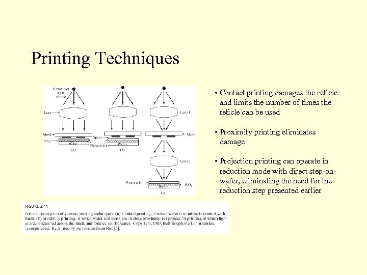 Printing Techniques • Contact printing damages the reticle and limits the number of times the reticle can be used • Proximity printing eliminates damage • Projection printing can operate in reduction mode with direct step-onwafer, eliminating the need for the reduction step presented earlier
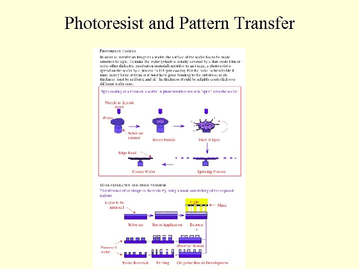 Photoresist and Pattern Transfer
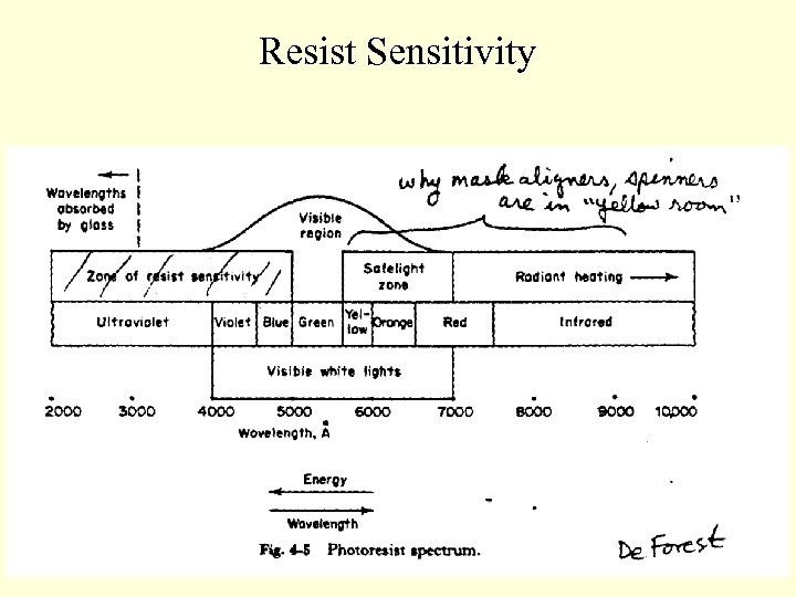 Resist Sensitivity
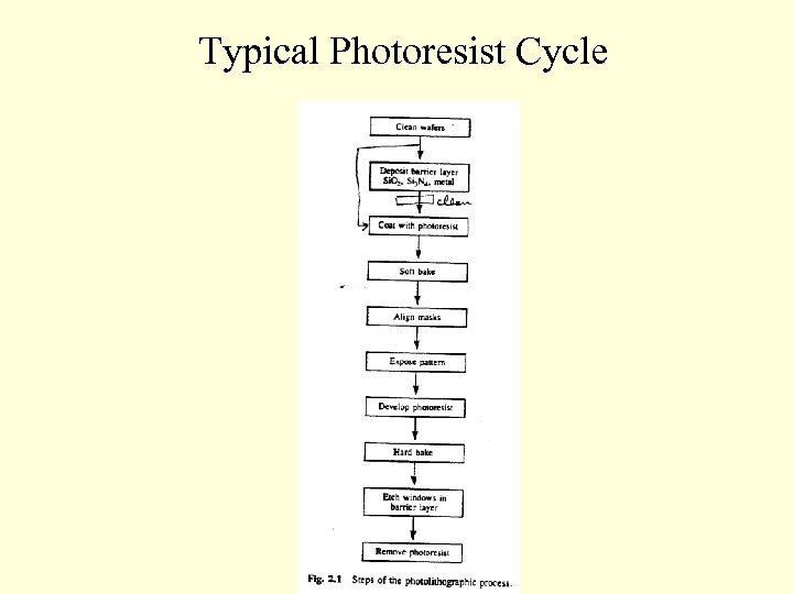 Typical Photoresist Cycle
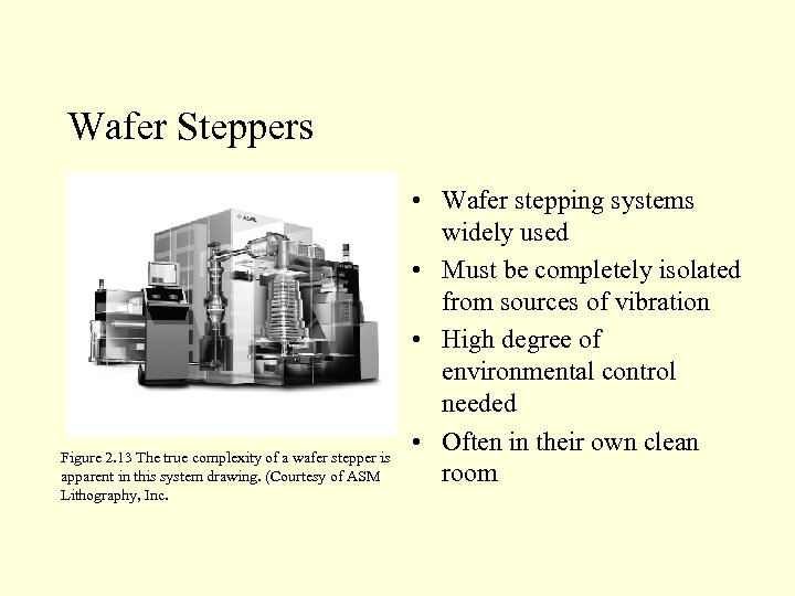 Wafer Steppers Figure 2. 13 The true complexity of a wafer stepper is apparent in this system drawing. (Courtesy of ASM Lithography, Inc. • Wafer stepping systems widely used • Must be completely isolated from sources of vibration • High degree of environmental control needed • Often in their own clean room
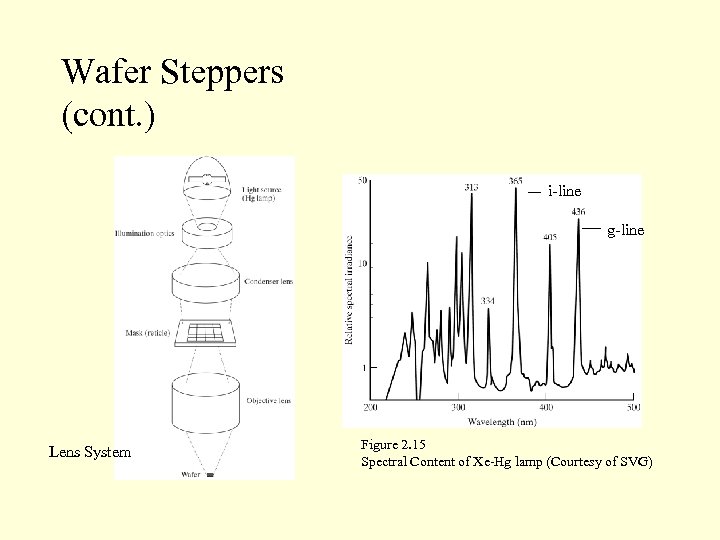 Wafer Steppers (cont. ) i-line g-line Lens System Figure 2. 15 Spectral Content of Xe-Hg lamp (Courtesy of SVG)
 Minimum Feature Size and Depth of Field
 ITRS Lithography Projections
 End of Lithography Slides for EE 3311
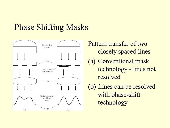 Phase Shifting Masks Pattern transfer of two closely spaced lines (a) Conventional mask technology - lines not resolved (b) Lines can be resolved with phase-shift technology
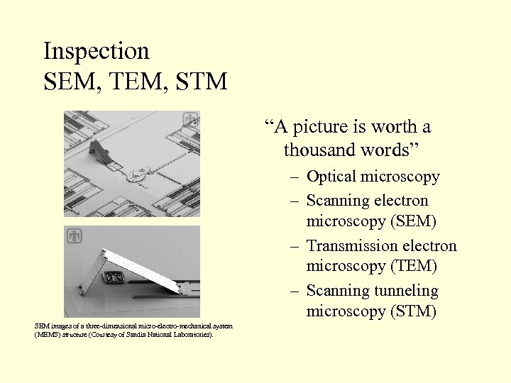 Inspection SEM, TEM, STM “A picture is worth a thousand words” – Optical microscopy – Scanning electron microscopy (SEM) – Transmission electron microscopy (TEM) – Scanning tunneling microscopy (STM) SEM images of a three-dimensional micro-electro-mechanical system (MEMS) structure (Courtesy of Sandia National Laboratories).
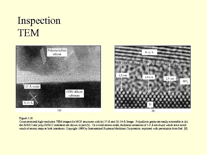 Inspection TEM Figure 2. 18 Cross-sectional high-resolution TEM images for MOS structures with (a) 27 -Å and (b) 24 -Å Image. Polysilicon grains are easily noticeable in (a); the Si/Si. O 2 and poly-Si/Si. O 2 interfaces are shown in part (b). On a local atomic scale, thickness variations of 2 -3 Å are found which are a direct result of atomic steps at both interfaces. Copyright 1969 by International Business Machines Corporation; reprinted with permission from Ref. [9].
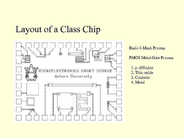 Layout of a Class Chip Basic 4 -Mask Process PMOS Metal-Gate Process 1. p-diffusion 2. Thin oxide 3. Contacts 4. Metal
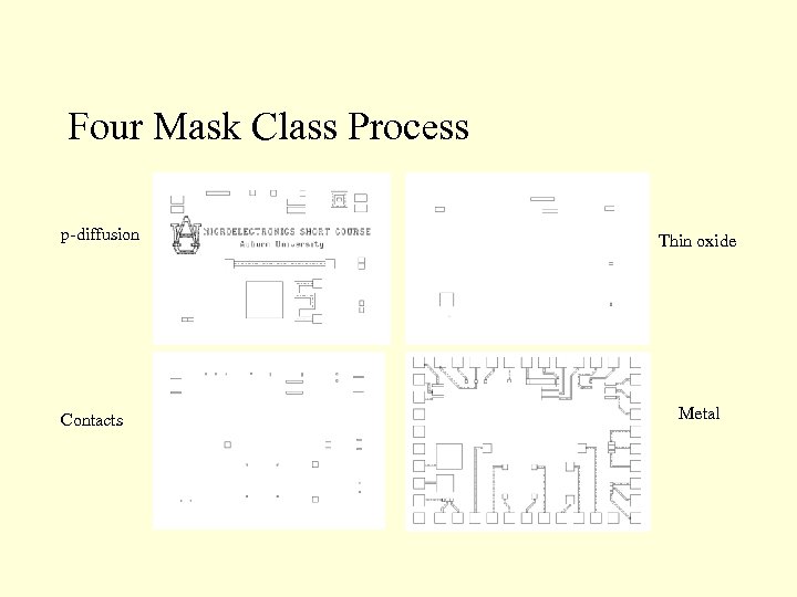 Four Mask Class Process p-diffusion Contacts Thin oxide Metal
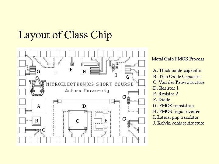 Layout of Class Chip Metal Gate PMOS Process G J F H I G G A D B C G E G A. Thick oxide capacitor B. Thin Oxide Capacitor C. Van der Pauw structure D. Resistor 1 E. Resistor 2 F. Diode G. PMOS transistors H. PMOS logic inverter I. Lateral pnp transistor J. Kelvin contact structure
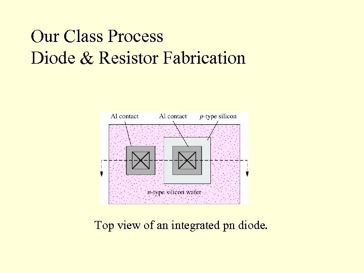 Our Class Process Diode & Resistor Fabrication Top view of an integrated pn diode.
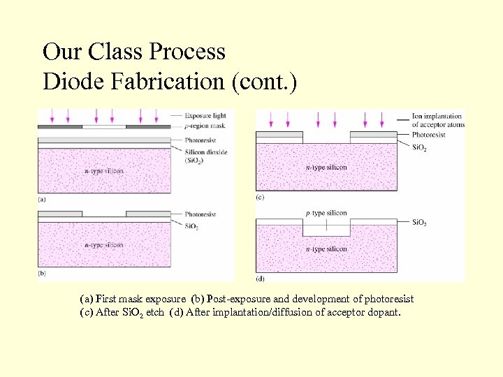 Our Class Process Diode Fabrication (cont. ) (a) First mask exposure (b) Post-exposure and development of photoresist (c) After Si. O 2 etch (d) After implantation/diffusion of acceptor dopant.
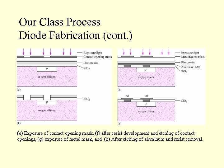 Our Class Process Diode Fabrication (cont. ) (e) Exposure of contact opening mask, (f) after resist development and etching of contact openings, (g) exposure of metal mask, and (h) After etching of aluminum and resist removal.
 Layout of Class Chip Metal Gate PMOS Process G J F H I G G A D B C G E G A. Thick oxide capacitor B. Thin Oxide Capacitor C. Van der Pauw structure D. Resistor 1 E. Resistor 2 F. Diode G. PMOS transistors H. PMOS logic inverter I. Lateral pnp transistor J. Kelvin contact structure
 References
 End of Lithography Section


