eed813358acbdc311f4877982855e496.ppt
- Количество слайдов: 40
 SME Initiative Critical processes related to electronic materials ESA SME Initiative Course D: Materials Ton de Rooij Principal Metallurgist Materials and Processes Division Product Assurance and Safety Department Materials and Processes Division ESA/ESTEC/TOS-QM 1
 SME Initiative Content of presentation • • • specifications pcb’s manufacturing soldering processes crimping wire wrapping Repair and modification of PCB assemblies cleaning quality evaluations good solderjoints failure modes Materials and Processes Division ESA/ESTEC/TOS-QM 2
 SME Initiative Specifications • ECSS-Q-70 -08 A – • ECSS-Q-70 -28 Space product assurance - manual soldering of high-reliability electrical connections • ECSS-Q-70 -10 – Space product assurance - qualification and procurement of multilayer printed circuit boards (gold plated or tin-lead finish) - to be published ( now ESA PSS-01 -710) • ESA PSS-01 -718 – Space product assurance - repair and modification of printed circuit board assemblies - to be published (now ESA PSS-01 -728) • ECSS-Q-70 -30 A – Space product assurance - wire-wrapping of highreliability electrical connections • ECSS-Q-70 -38 – the preparation, assembly and mounting of RF coaxial cables • ECSS-Q-70 -26 – – Space product assurance - high-reliability soldering for surface mount and mixed technology printed circuit boards - to be published (now ESA PSS-01738) Space product assurance - the crimping of highreliability electrical connections -to be published (now ESA PSS-01 -726) Materials and Processes Division ESA/ESTEC/TOS-QM 3
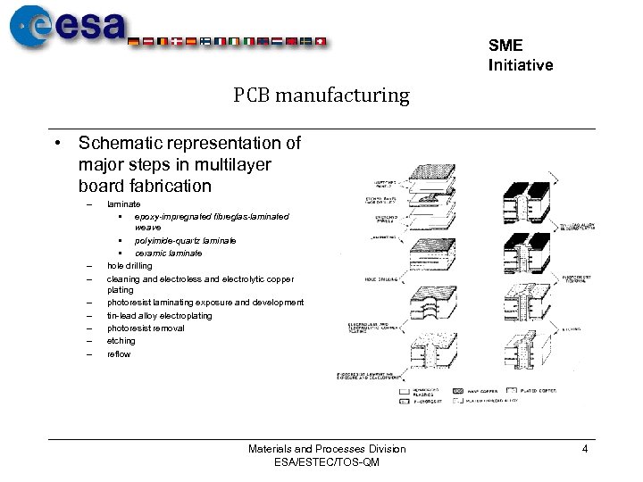 SME Initiative PCB manufacturing • Schematic representation of major steps in multilayer board fabrication – – – – laminate • epoxy-impregnated fibreglas-laminated weave • polyimide-quartz laminate • ceramic laminate hole drilling cleaning and electroless and electrolytic copper plating photoresist laminating exposure and development tin-lead alloy electroplating photoresist removal etching reflow Materials and Processes Division ESA/ESTEC/TOS-QM 4
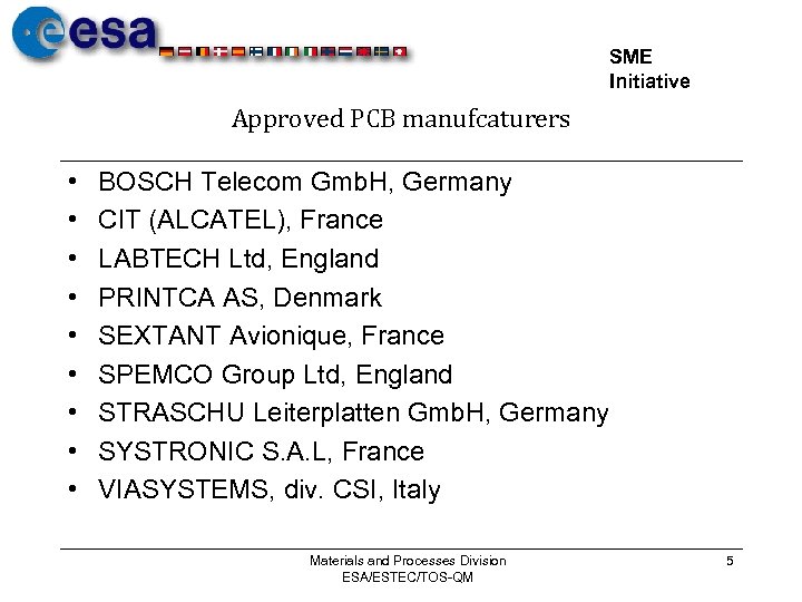 SME Initiative Approved PCB manufcaturers • • • BOSCH Telecom Gmb. H, Germany CIT (ALCATEL), France LABTECH Ltd, England PRINTCA AS, Denmark SEXTANT Avionique, France SPEMCO Group Ltd, England STRASCHU Leiterplatten Gmb. H, Germany SYSTRONIC S. A. L, France VIASYSTEMS, div. CSI, Italy Materials and Processes Division ESA/ESTEC/TOS-QM 5
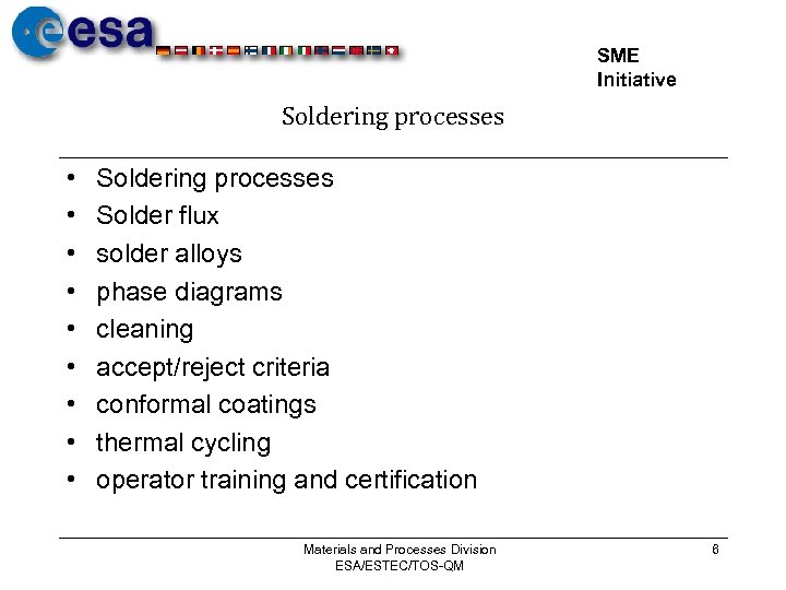 SME Initiative Soldering processes • • • Soldering processes Solder flux solder alloys phase diagrams cleaning accept/reject criteria conformal coatings thermal cycling operator training and certification Materials and Processes Division ESA/ESTEC/TOS-QM 6
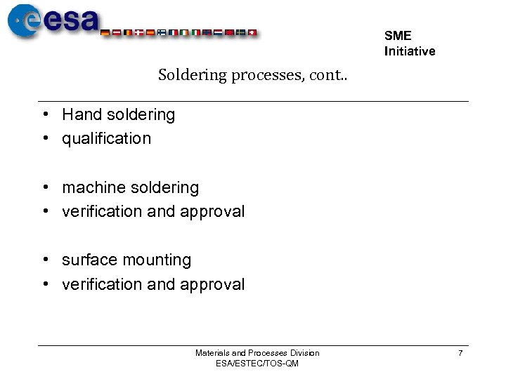 SME Initiative Soldering processes, cont. . • Hand soldering • qualification • machine soldering • verification and approval • surface mounting • verification and approval Materials and Processes Division ESA/ESTEC/TOS-QM 7
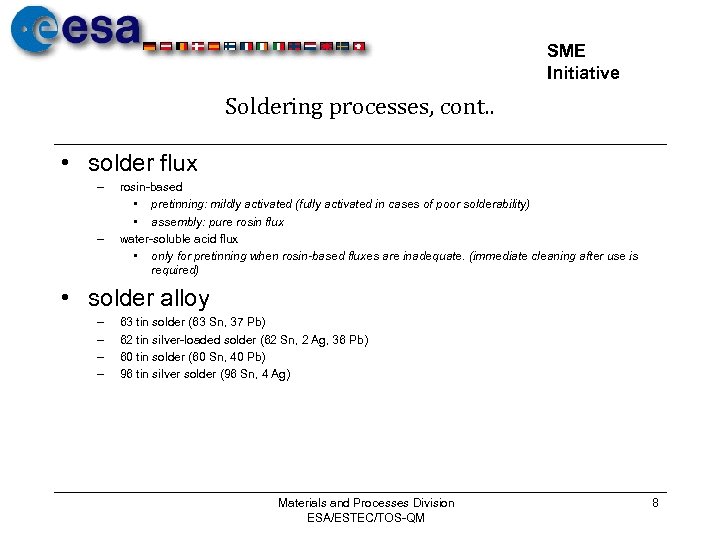 SME Initiative Soldering processes, cont. . • solder flux – – rosin-based • pretinning: mildly activated (fully activated in cases of poor solderability) • assembly: pure rosin flux water-soluble acid flux • only for pretinning when rosin-based fluxes are inadequate. (immediate cleaning after use is required) • solder alloy – – 63 tin solder (63 Sn, 37 Pb) 62 tin silver-loaded solder (62 Sn, 2 Ag, 36 Pb) 60 tin solder (60 Sn, 40 Pb) 96 tin silver solder (96 Sn, 4 Ag) Materials and Processes Division ESA/ESTEC/TOS-QM 8
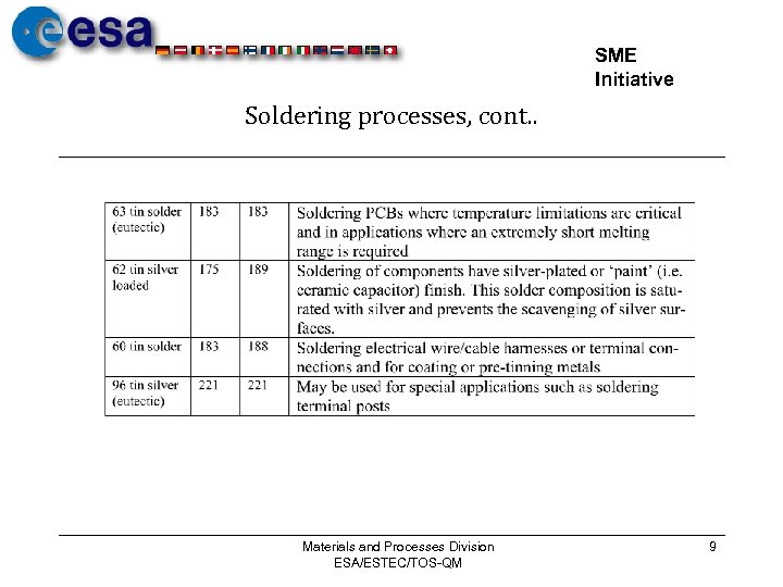 SME Initiative Soldering processes, cont. . Materials and Processes Division ESA/ESTEC/TOS-QM 9
 SME Initiative Soldering processes, cont. . • Cleaning – solvents shall be non-corrosive and non-conductive and shall not degrade parts or materials. • Acceptable solvents are: – – ethyl alcohol (99. 5% or 95% pure by volume) isopropyl alcohol (best commercial grade, 99% pure) deionized water at 40 o. C maximum for certain fluxes (dry after use) any mixture of the above Materials and Processes Division ESA/ESTEC/TOS-QM 10
 SME Initiative Principles of reliable soldered connections • Reliable soldered connections result from proper design, control of tools, materials and work environments, and careful workmanship • basic deign concepts: – – – stress relief shall be inherent in the design where adequate stress relief is not possible, solder-joint reinforcement is necessary materials shall be so selected that the mismatch of thermal expansion coefficient is minimal materials and processes which the formation of brittle intermetallic shall be avoided the design shall permit inspection of the soldered joints Materials and Processes Division ESA/ESTEC/TOS-QM 11
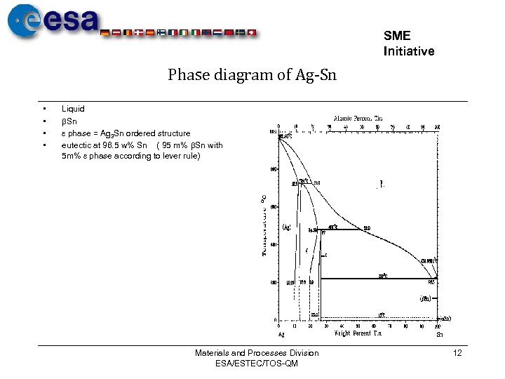 SME Initiative Phase diagram of Ag-Sn • • Liquid Sn phase = Ag 3 Sn ordered structure eutectic at 96. 5 w% Sn ( 95 m% Sn with 5 m% phase according to lever rule) Materials and Processes Division ESA/ESTEC/TOS-QM 12
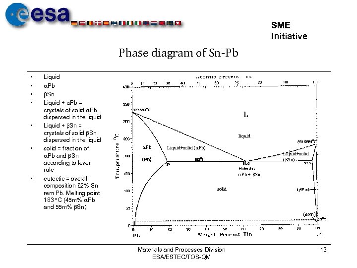 SME Initiative Phase diagram of Sn-Pb • • Liquid Pb Sn Liquid + Pb = crystals of solid Pb dispersed in the liquid Liquid + Sn = crystals of solid Sn dispersed in the liquid solid = fraction of Pb and Sn according to lever rule eutectic = overall composition 62% Sn rem Pb. Melting point 183 o. C (45 m% Pb and 55 m% Sn) liquid Pb Liquid+solid ( Pb) Liquid+solid ( Sn) Eutectic Pb + Sn solid Materials and Processes Division ESA/ESTEC/TOS-QM 13
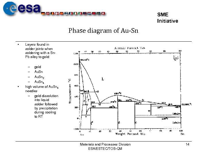 SME Initiative Phase diagram of Au-Sn • • Layers found in solder joints when soldering with a Sn. Pb alloy to gold: – gold – Au. Sn 2 – Au. Sn 4 high volume of Au. Sn 4 needles – gold dissolution into liquid solder followed by precipitation during cooling to RT Materials and Processes Division ESA/ESTEC/TOS-QM 14
 SME Initiative Acceptance criteria • Clean, smooth, bright undisturbed surface • solder fillets between conductor and termination areas as illustrated • contour of wire sufficiently visible to determine presence of wire • complete wetting as evidenced by a low contact angle • proper amount and distribution of solder • absence of defects as mentioned in the next sheet Materials and Processes Division ESA/ESTEC/TOS-QM 15
 SME Initiative Rejection criteria – – – – – Charred, burned, or melted insulation of parts conductor pattern separation for board burns on base material discoloration which is continuous between two conductors excessive solder (peaks, bridging) flux residue, solder spatter, or other foreign matter dewetting insufficient solder pits, holes or voids, or exposed base metal in the solder connection granular or disturbed solder joints – – – – fractured or cracked solder connections cut, nicked, gouged, or scraped conductors or conductor pattern improper conductor length or direction of clinch and lap termination repaired or damaged conductor pattern(rework if applicable) bare copper or base metal (except end of cut wire or leads) soldered joints made directly to gold-plated terminals and conductors cold solder joints component moulding with solder fillet Materials and Processes Division ESA/ESTEC/TOS-QM 16
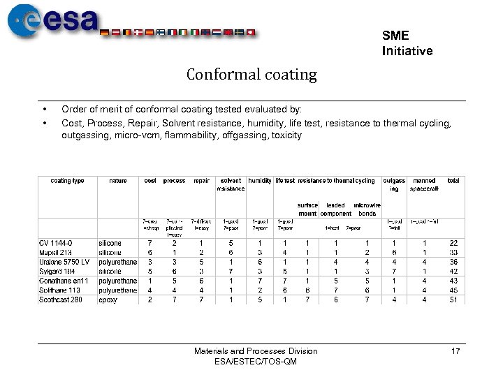 SME Initiative Conformal coating • • Order of merit of conformal coating tested evaluated by: Cost, Process, Repair, Solvent resistance, humidity, life test, resistance to thermal cycling, outgassing, micro-vcm, flammability, offgassing, toxicity Materials and Processes Division ESA/ESTEC/TOS-QM 17
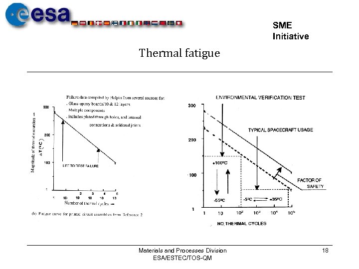 SME Initiative Thermal fatigue Materials and Processes Division ESA/ESTEC/TOS-QM 18
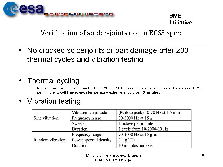 SME Initiative Verification of solder-joints not in ECSS spec. • No cracked solderjoints or part damage after 200 thermal cycles and vibration testing • Thermal cycling – temperature cycling in air from RT to -55 o. C to +100 o. C and back to RT at a rate not to exceed 10 o. C per minute. Dwell time at each temperature extreme should be 15 minutes. • Vibration testing Materials and Processes Division ESA/ESTEC/TOS-QM 19
 SME Initiative Operator and inspector training and certification • Trained and competent personnel shall be employed for all soldering operations and inspections • Trained personnel performing soldering operations and inspection shall be certified at a soldering school – – – ZVE, Oberpfaffenhofen, Germany Highbury College, Portsmouth, England Italian Institute of welding (IIS), Genova, Italy IFE, Oberpfaffenhofen, Germany Hytek, Aalborg, Denmark Institute de soudure, Paris, France Materials and Processes Division ESA/ESTEC/TOS-QM 20
 SME Initiative Training programmes • • Hand soldering to ESA PSS-01 -708 inspection of solder joints repair and modification of pcb’s to ESA PSS-01 -728 RF cable assembly to ESA PSS-01 -718 crimping and wire wrapping to ESA PSS-01 -726/730 surface mounting techn. Ass. To ESA PSS-01 -738 Instructor cat 1 to ESA PSS-01 -748 fiber optic terminations to ESA-draft/NASA-std-8739. 5 Materials and Processes Division ESA/ESTEC/TOS-QM 21
 SME Initiative Soldering of surface mount devices to pcb’s ESA PSS-01 -738 • Request for verification • technology sample • process identification document and process control sheet • audit of assembly line • verification programme • smd assembly approval Materials and Processes Division ESA/ESTEC/TOS-QM 22
 SME Initiative Soldering of surface mount devices to pcb’s, cont. . • Request for verification – The verification of any SMD assembly line will be restricted to those companies which have been selected for the fabrication of ESA sponsored projects. • Technology sample – the contractor will supply one sample from his SMD assembly process to ESTEC. This sample will be examined at ESTEC or a recognised test house • no conformal coating • workmanship • cleanliness • metallography of soldered interconnections • Audit of assembly process line – – following acceptance of the technology sample the manufacturing facility will be audited by ESA findings of the audit remain as confidential to ESA Materials and Processes Division ESA/ESTEC/TOS-QM 23
 SME Initiative Soldering of surface mount devices to pcb’s, cont. . • Verification programme – – Details of verification programme will be discussed at the time of the audit • acc. To ESA PSS-01 -738 • thermal cycling (500: -55 to +100 o. C) • vibration • visual, electrical test, cleanliness test, microsection control the verification programme shall be established and approved by ESA the verification programme shall be funded and performed by the contractor or one or more independent test houses (test house require approval by ESA) summary table for SMD verified to ESA PSS-01 -738 shall be compiled • SMD assembly approval – – following the successful completion of the verification programme a letter of approval will be issued by ESA project approval by means of Project Declared Process List The summary table for SMD’s will be attached to this letter The validation period is indefinite until change to PID history of supply, manufacturing defects and unauthorised change of materials and or manufacturing methods will require new verification Materials and Processes Division ESA/ESTEC/TOS-QM 24
 SME Initiative Automatic machine wave soldering • ECSS-Q-70 -07 A • verification tests to establish confidence in all automatic machine soldering lines • technology samples – – technology samples, cleanliness, documentation examination by recognised test house • line audit • verification testing – – – testing according to ECSS-Q-70 -70 A: visual inspection, electrical tests, thermal cycling, vibration when design deviates from ECSS-Q-70 -08 microsectioning pull testing of leads on board surface Materials and Processes Division ESA/ESTEC/TOS-QM 25
 SME Initiative high-reliability electrical connections • CRIMPING – Forms of crimps – Crimping optimisation – Workmanship examples • WIRE WRAPPING – – wire types recommended insulations terminal posts examples Materials and Processes Division ESA/ESTEC/TOS-QM 26
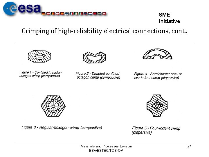 SME Initiative Crimping of high-reliability electrical connections, cont. . Materials and Processes Division ESA/ESTEC/TOS-QM 27
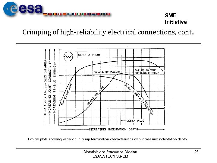 SME Initiative Crimping of high-reliability electrical connections, cont. . Typical plots showing variation in crimp termination characteristics with increasing indentation depth Materials and Processes Division ESA/ESTEC/TOS-QM 28
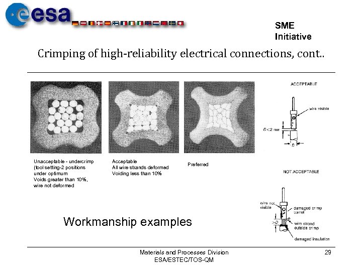 SME Initiative Crimping of high-reliability electrical connections, cont. . Unacceptable - undercrimp (tool setting-2 positions under optimum Voids greater than 10%, wire not deformed Acceptable All wire strands deformed Voiding less than 10% Preferred Workmanship examples Materials and Processes Division ESA/ESTEC/TOS-QM 29
 SME Initiative Wire-wrapping of high-rel. electrical connections • Wire used for wrapped connections shall conform to ESA/SCC No. 3903 or other approved national wire specification intended for wire wrapping – – – the wire shall be a single solid round conductor. Stranded conductors shall not be used Conductor size shall be between AWG 24 and AWG 30 • soft annealed high-conductivity copper for AWG 28 and AWG 30 • high strength high-conductivity copper for wire gauges AWG 28 and AWG 30 copper shall be silver plated (>2 micron) • Recommended wire insulations – – outgassing according to ECSS-Q-70 -02 ETFE (Tefzel), PFA (Perfluoroalkoxy), PVDF (Kynar), and Kapton poluimide over extruded PTFE • Terminal post – – suitable grades of copper or nickel alloys (Copper-Zinc, Phosphor-bronze, copper-nickel-zinc, beryllium-copper, nickel-copper(Monel) and nickel-cclad copper(Kulgrid) 1 to 3 microns of Gold over min. 1 micron of copper or nickel (barrier plating). No Silver undeplating Materials and Processes Division ESA/ESTEC/TOS-QM 30
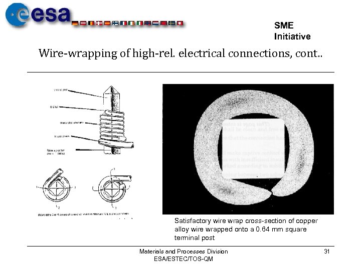 SME Initiative Wire-wrapping of high-rel. electrical connections, cont. . Satisfactory wire wrap cross-section of copper alloy wire wrapped onto a 0. 64 mm square terminal post Materials and Processes Division ESA/ESTEC/TOS-QM 31
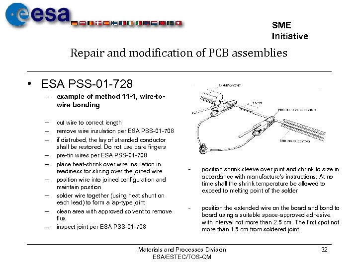 SME Initiative Repair and modification of PCB assemblies • ESA PSS-01 -728 – example of method 11 -1, wire-towire bonding – – – – – cut wire to correct length remove wire insulation per ESA PSS-01 -708 if distrubed, the lay of stranded conductor shall be restored. Do not use bare fingers pre-tin wires per ESA PSS-01 -708 place heat-shrink over wire insulation in readiness for slicing over the joined wire position wire into joined configuration and maintain position solder wire together (using heat shunt on each lead) to form a lap-type joint clean area with approved solvent to remove flux inspect joint per ESA PSS-01 -708 - position shrink sleeve over joint and shrink to size in accordance with manufacture’s instructions. At no time shall the shrink temperature be allowed to exceed to melting point of the solder - position the extended wire on the board and bond to board using a suitable space-approved adhesive, with interval not more than 2. 5 cm. The first spot not more than 1. 5 cm from soldered joint Materials and Processes Division ESA/ESTEC/TOS-QM 32
 SME Initiative Examples of solderjoints • • • Good quality solderjoints Good quality SMT solderjoints Cross section of smd devices soldering to gold No pretinning After thermal cycling • whisker growth on Tin-plated brass Materials and Processes Division ESA/ESTEC/TOS-QM 33
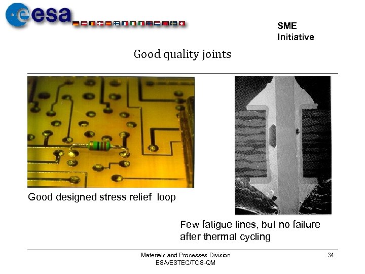 SME Initiative Good quality joints Good designed stress relief loop Few fatigue lines, but no failure after thermal cycling Materials and Processes Division ESA/ESTEC/TOS-QM 34
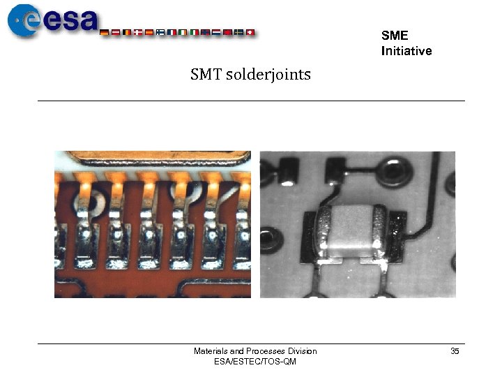 SME Initiative SMT solderjoints Materials and Processes Division ESA/ESTEC/TOS-QM 35
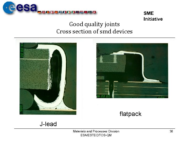 Good quality joints Cross section of smd devices SME Initiative flatpack J-lead Materials and Processes Division ESA/ESTEC/TOS-QM 36
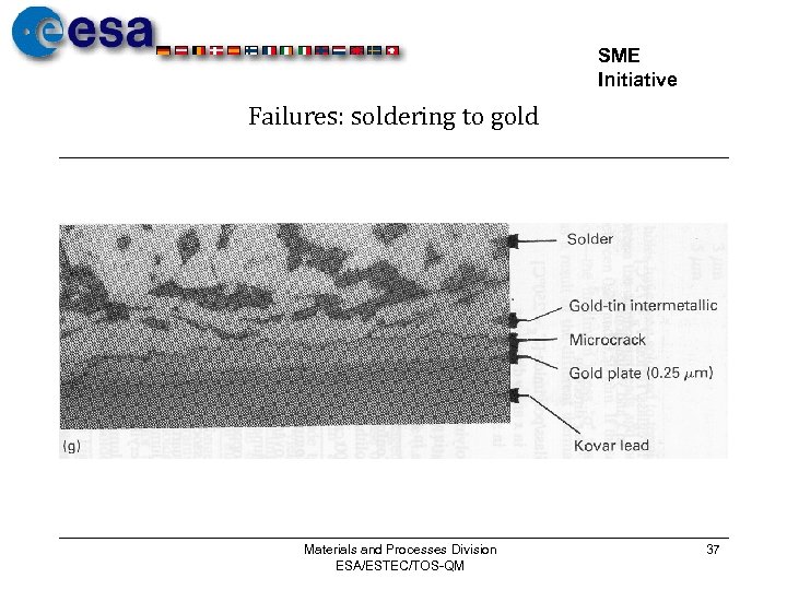 SME Initiative Failures: soldering to gold Materials and Processes Division ESA/ESTEC/TOS-QM 37
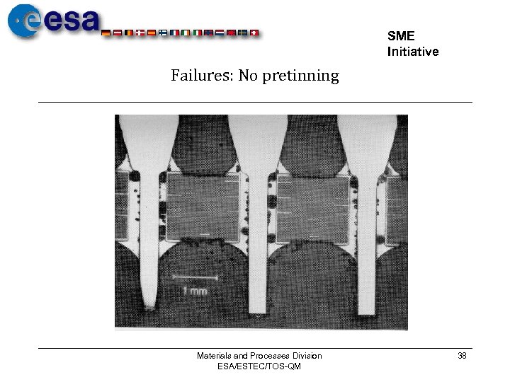 SME Initiative Failures: No pretinning Materials and Processes Division ESA/ESTEC/TOS-QM 38
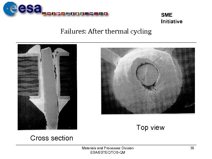 SME Initiative Failures: After thermal cycling Top view Cross section Materials and Processes Division ESA/ESTEC/TOS-QM 39
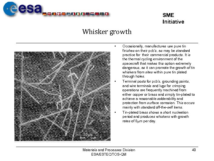 SME Initiative Whisker growth • • • Occasionally, manufactures use pure tin finishes on their pcb’s, as may be standard practice for their commercial products. It is thermal cycling environment of the spacecraft that makes this option extremely dangerous, as it can promote the growth of tin whiskers from sites within pure tin plated through holes. Terminal posts for pcb’s, grounding points, and wire terminals and lugs for crimping operations are frequently machined from either copper or brass and simply tin-plated to achieve a reasonable solderability and protection from surface corrosion. This occurs mainly with standard off-the-self items. Tin-plated brass shows a short nucleation period and produces whiskers with growth rates of 8 m per day. Materials and Processes Division ESA/ESTEC/TOS-QM 40


