fa2c9ba9c699d9d3cb4c6aa343fa3c3f.ppt
- Количество слайдов: 22
SHAPES: a tiled scalable Software Hardware Architecture Platform for Embedded Systems HW overview P. S. Paolucci (INFN and Atmel Roma) for the SHAPES Consortium Coordinator of the European Project Permanent Staff Researcher (part time) Istituto Nazionale di Fisica Nucleare Roma – Italy 4 generations of APE Massive Parallel Processors based on custom VLIW DSP (part time) Technology Director and Founder ATMEL Roma, corporate design center of ATMEL for Advanced DSP 2 generations of RISC + custom m. Agic VLIW DSP MPSo. C Pier Stanislao Paolucci - Atmel Roma and INFN Roma - SHAPES HW Overview 1
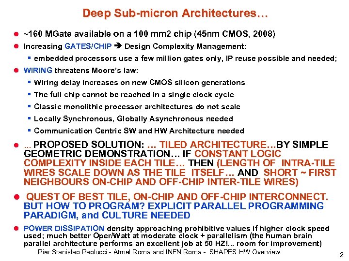
Deep Sub-micron Architectures… l ~160 MGate available on a 100 mm 2 chip (45 nm CMOS, 2008) l Increasing GATES/CHIP Design Complexity Management: § embedded processors use a few million gates only, IP reuse possible and needed; l WIRING threatens Moore’s law: § Wiring delay increases on new CMOS silicon generations § The full chip cannot be reached in a single clock cycle § Classic monolithic processor architectures do not scale § Locally Synchronous, Globally Asynchronous needed § Communication Centric SW and HW Architecture needed l … PROPOSED SOLUTION: … TILED ARCHITECTURE…BY SIMPLE GEOMETRIC DEMONSTRATION… IF CONSTANT LOGIC COMPLEXITY INSIDE EACH TILE… THEN (LENGTH OF INTRA-TILE WIRES SCALE DOWN AS THE TILE ITSELF… AND SHORT ~ FIRST NEIGHBOURS ON-CHIP AND OFF-CHIP INTER-TILE WIRES) l QUEST OF BEST TILE, ON-CHIP AND OFF-CHIP INTERCONNECT. BUT HOW TO PROGRAM? EXPLICIT PARALLEL PROGRAMMING PARADIGM, and CULTURE NEEDED l POWER DISSIPATION density approaching prohibitive values if higher clock speed used; much better Oper/Watt at moderate clock + parallelism (the human brain parallel architecture performs an excellent job at 50 HZ!. . . room for improvement) Pier Stanislao Paolucci - Atmel Roma and INFN Roma - SHAPES HW Overview 2
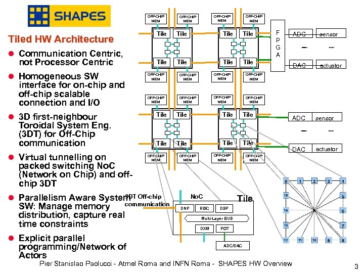
OFF-CHIP MEM Tile Tiled HW Architecture Tile l Communication Centric, not Processor Centric l Homogeneous SW interface for on-chip and off-chip scalable connection and I/O OFF-CHIP MEM OFF-CHIP MEM l Virtual tunnelling on packed switching No. C (Network on Chip) and offchip 3 DT Tile Tile DAC Tile OFF-CHIP MEM communication OFF-CHIP MEM 3 DT l Parallelism Aware System Off-chip SW: Manage memory distribution, capture real time constraints sensor actuator OFF-CHIP MEM Tile Toroidal System Eng. (3 DT) for Off-Chip communication ADC OFF-CHIP MEM Tile l 3 D first-neighbour F P G A No. C DNP RISC ADC sensor DAC actuator OFF-CHIP MEM Tile DSP Multi-Layer BUS DXM POT l Explicit parallel programming/Network of Actors ADC/DAC Pier Stanislao Paolucci - Atmel Roma and INFN Roma - SHAPES HW Overview 3
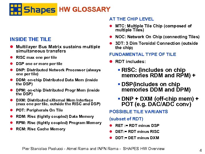
HW GLOSSARY AT THE CHIP LEVEL l MTC: Multiple Tile Chip (composed of multiple Tiles) INSIDE THE TILE l Multilayer Bus Matrix sustains multiple simultaneous transfers l RISC max one per tile l DSP one or more per tile l DNP: Distributed Network Processor (always one per tile) l DDM: on-chip Distributed Data Mem (inside the DSP) l DPM: on-chip Distributed Progr Mem (inside the DSP) l DXM: Distributed e. Xternal Mem Interface (max one per tile, outside the RISC and DSP) l POT: Peripherals On Tile l RDM: Risc (tightly coupled) Data Memory l RPM: Risc (tightly coupled) Program Memory l RCM: Risc Cache Memory l NOC: Network On Chip (connecting Tiles) l 3 DT: 3 Dim Toroidal Connection (outside the chip) FUNDAMENTAL TYPE OF TILE l RDT includes: § RISC: (includes on chip memories RDM and RPM) + § DSP(includes on chip memories DDM and DPM) § DNP + DXM (off-chip mem) + POT (e. g. DAC/ADC conv) POSSIBLE TILE VARIANTS (subset of RDT) l RET : = RDT minus DSP l DET: = RDT minus RISC l DDT: = DET minus DXM Pier Stanislao Paolucci - Atmel Roma and INFN Roma - SHAPES HW Overview 4
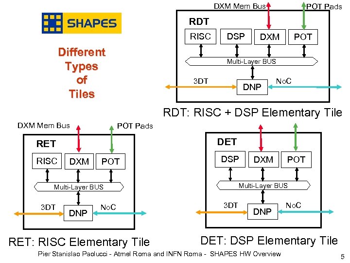
DXM Mem Bus POT Pads RDT RISC Different Types of Tiles DSP DXM POT Multi-Layer BUS 3 DT DNP No. C RDT: RISC + DSP Elementary Tile DXM Mem Bus POT Pads DET RISC DXM POT DSP DNP No. C RET: RISC Elementary Tile POT Multi-Layer BUS 3 DT DXM 3 DT DNP No. C DET: DSP Elementary Tile Pier Stanislao Paolucci - Atmel Roma and INFN Roma - SHAPES HW Overview 5
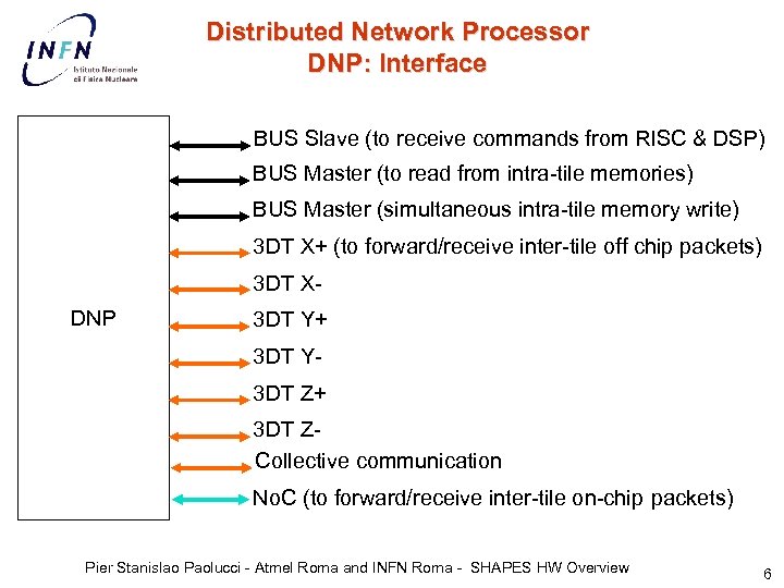
Distributed Network Processor DNP: Interface BUS Slave (to receive commands from RISC & DSP) BUS Master (to read from intra-tile memories) BUS Master (simultaneous intra-tile memory write) 3 DT X+ (to forward/receive inter-tile off chip packets) 3 DT XDNP 3 DT Y+ 3 DT Y 3 DT Z+ 3 DT ZCollective communication No. C (to forward/receive inter-tile on-chip packets) Pier Stanislao Paolucci - Atmel Roma and INFN Roma - SHAPES HW Overview 6
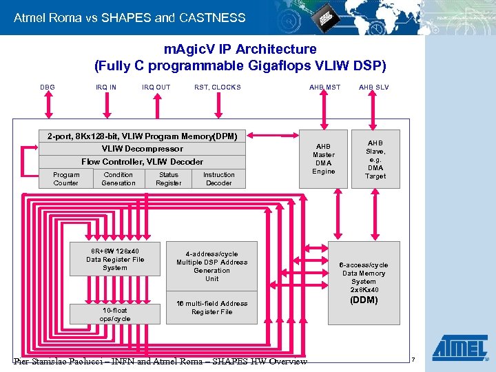
Atmel Roma vs SHAPES and CASTNESS m. Agic. V IP Architecture (Fully C programmable Gigaflops VLIW DSP) DBG IRQ IN IRQ OUT RST, CLOCKS AHB MST AHB SLV AHB Master DMA Engine AHB Slave, e. g. DMA Target 2 -port, 8 Kx 128 -bit, VLIW Program Memory(DPM) VLIW Decompressor Flow Controller, VLIW Decoder Program Counter Condition Generation 8 R+8 W 128 x 40 Data Register File System 10 -float ops/cycle Status Register Instruction Decoder 4 -address/cycle Multiple DSP Address Generation Unit 16 multi-field Address Register File Pier Stanislao Paolucci – INFN and Atmel Roma – SHAPES HW Overview 6 -access/cycle Data Memory System 2 x 8 Kx 40 (DDM) 7
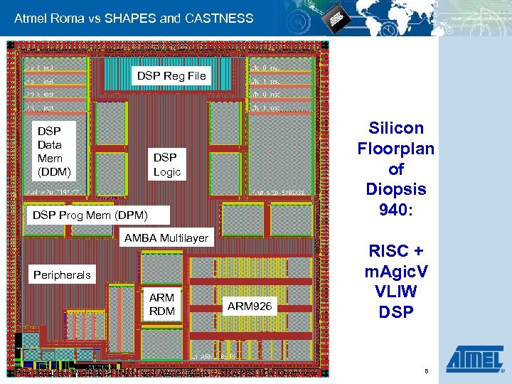
Atmel Roma vs SHAPES and CASTNESS DSP Reg File DSP Data Mem (DDM) Silicon Floorplan of Diopsis 940: DSP Logic DSP Prog Mem (DPM) AMBA Multilayer Peripherals ARM RDM ARM 926 Pier Stanislao Paolucci – INFN and Atmel Roma – SHAPES HW Overview RISC + m. Agic. V VLIW DSP 8
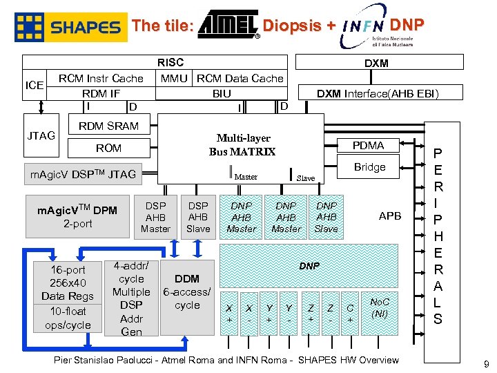
RCM Instr Cache RDM IF I D ICE JTAG DNP Diopsis + The tile: RISC MMU RCM Data Cache BIU D I DXM Interface(AHB EBI) RDM SRAM Multi-layer Bus MATRIX ROM m. Agic. V DSPTM JTAG m. Agic. VTM DPM 2 -port 16 -port 256 x 40 Data Regs 10 -float ops/cycle PDMA Bridge Master DSP AHB Master 4 -addr/ cycle Multiple DSP Addr Gen DSP AHB Slave DNP AHB Master APB DNP DDM 6 -access/ cycle X + X - Y + Y - Z + Z - C + No. C (NI) Pier Stanislao Paolucci - Atmel Roma and INFN Roma - SHAPES HW Overview P E R I P H E R A L S 9
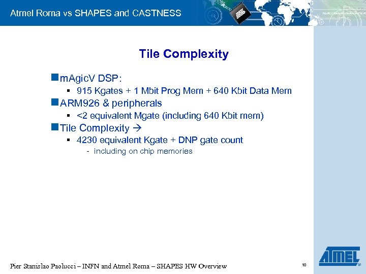
Atmel Roma vs SHAPES and CASTNESS Tile Complexity n m. Agic. V DSP: § 915 Kgates + 1 Mbit Prog Mem + 640 Kbit Data Mem n ARM 926 & peripherals § <2 equivalent Mgate (including 640 Kbit mem) n Tile Complexity § 4230 equivalent Kgate + DNP gate count - including on chip memories Pier Stanislao Paolucci – INFN and Atmel Roma – SHAPES HW Overview 10
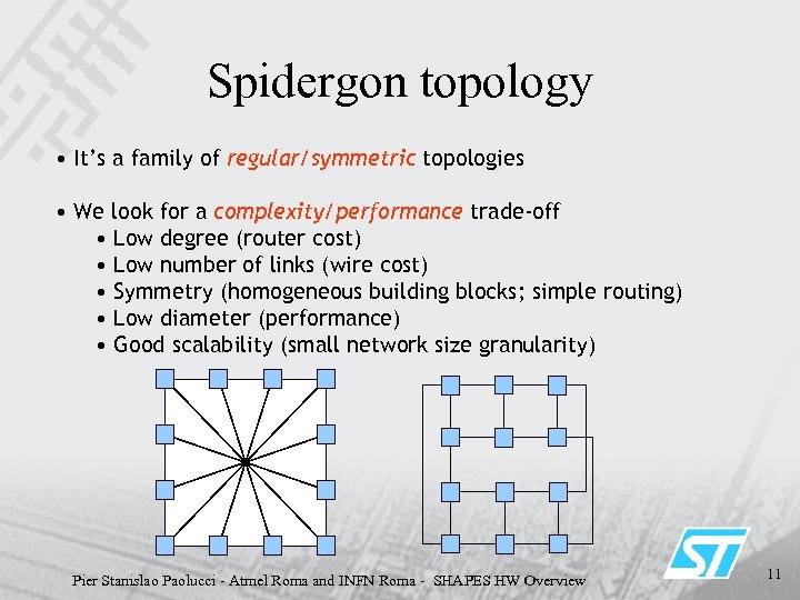
Spidergon topology • It’s a family of regular/symmetric topologies • We look for a complexity/performance trade-off • Low degree (router cost) • Low number of links (wire cost) • Symmetry (homogeneous building blocks; simple routing) • Low diameter (performance) • Good scalability (small network size granularity) Pier Stanislao Paolucci - Atmel Roma and INFN Roma - SHAPES HW Overview 11
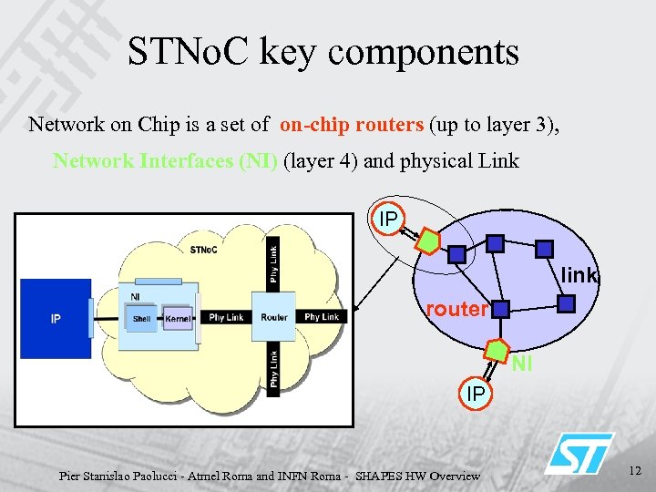
STNo. C key components Network on Chip is a set of on-chip routers (up to layer 3), Network Interfaces (NI) (layer 4) and physical Link IP link router NI IP Pier Stanislao Paolucci - Atmel Roma and INFN Roma - SHAPES HW Overview 12
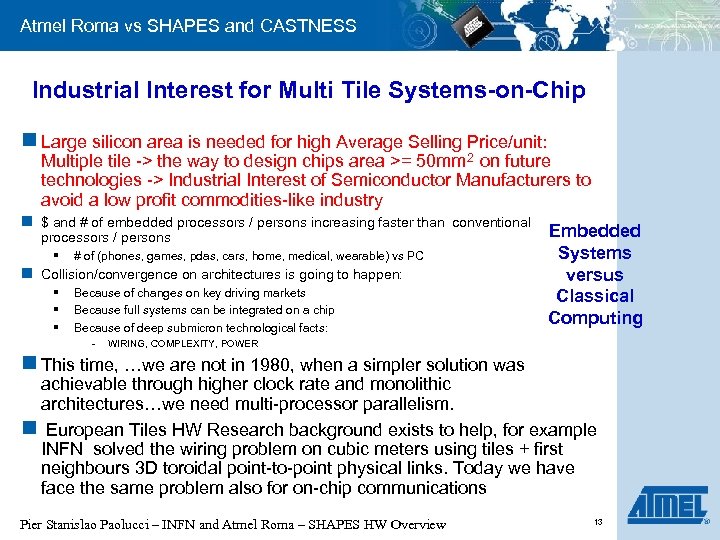
Atmel Roma vs SHAPES and CASTNESS Industrial Interest for Multi Tile Systems-on-Chip n Large silicon area is needed for high Average Selling Price/unit: Multiple tile -> the way to design chips area >= 50 mm 2 on future technologies -> Industrial Interest of Semiconductor Manufacturers to avoid a low profit commodities-like industry n $ and # of embedded processors / persons increasing faster than conventional processors / persons § # of (phones, games, pdas, cars, home, medical, wearable) vs PC n Collision/convergence on architectures is going to happen: § § § Because of changes on key driving markets Because full systems can be integrated on a chip Because of deep submicron technological facts: - Embedded Systems versus Classical Computing WIRING, COMPLEXITY, POWER n This time, …we are not in 1980, when a simpler solution was achievable through higher clock rate and monolithic architectures…we need multi-processor parallelism. n European Tiles HW Research background exists to help, for example INFN solved the wiring problem on cubic meters using tiles + first neighbours 3 D toroidal point-to-point physical links. Today we have face the same problem also for on-chip communications Pier Stanislao Paolucci – INFN and Atmel Roma – SHAPES HW Overview 13
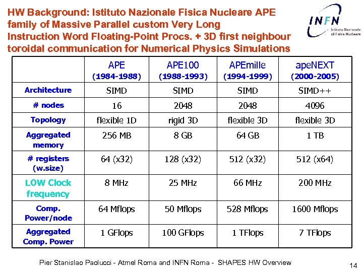
HW Background: Istituto Nazionale Fisica Nucleare APE family of Massive Parallel custom Very Long Instruction Word Floating-Point Procs. + 3 D first neighbour toroidal communication for Numerical Physics Simulations APE 100 APEmille ape. NEXT (1984 -1988) (1988 -1993) (1994 -1999) (2000 -2005) Architecture SIMD++ # nodes 16 2048 4096 Topology flexible 1 D rigid 3 D flexible 3 D Aggregated memory 256 MB 8 GB 64 GB 1 TB # registers (w. size) 64 (x 32) 128 (x 32) 512 (x 64) LOW Clock frequency 8 MHz 25 MHz 66 MHz 200 MHz Comp. Power/node 64 Mflops 50 Mflops 528 Mflops 1600 Mflops Aggregated Comp. Power 1 GFlops 100 GFlops 1 TFlops 7 TFlops Pier Stanislao Paolucci - Atmel Roma and INFN Roma - SHAPES HW Overview 14
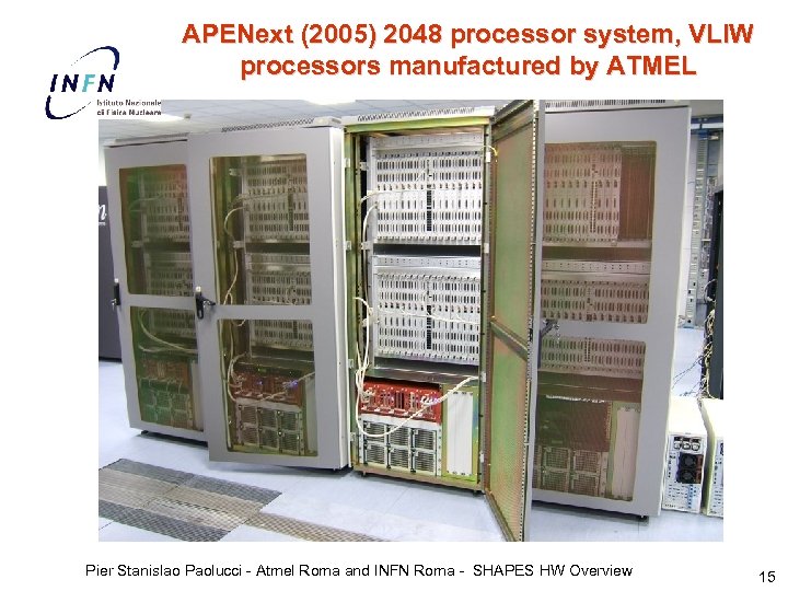
APENext (2005) 2048 processor system, VLIW processors manufactured by ATMEL Pier Stanislao Paolucci - Atmel Roma and INFN Roma - SHAPES HW Overview 15
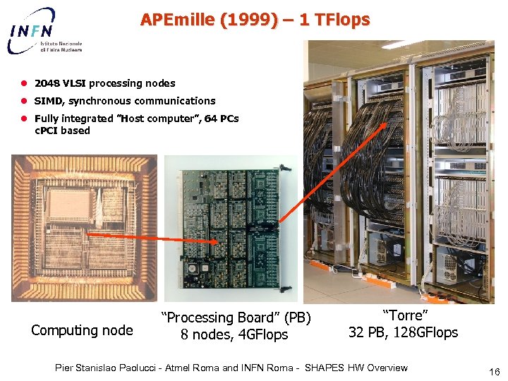
APEmille (1999) – 1 TFlops l 2048 VLSI processing nodes l SIMD, synchronous communications l Fully integrated ”Host computer”, 64 PCs c. PCI based Computing node “Processing Board” (PB) 8 nodes, 4 GFlops “Torre” 32 PB, 128 GFlops Pier Stanislao Paolucci - Atmel Roma and INFN Roma - SHAPES HW Overview 16
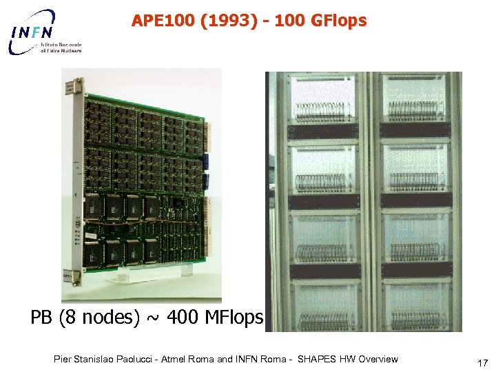
APE 100 (1993) - 100 GFlops PB (8 nodes) ~ 400 MFlops Pier Stanislao Paolucci - Atmel Roma and INFN Roma - SHAPES HW Overview 17
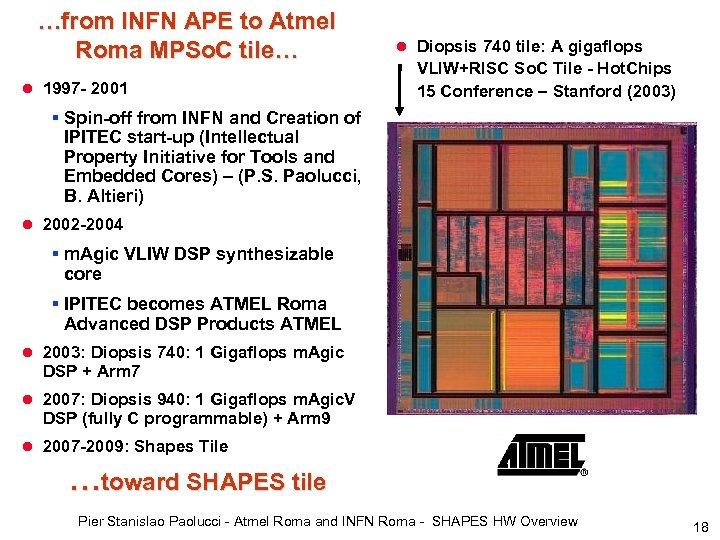
…from INFN APE to Atmel Roma MPSo. C tile… l 1997 - 2001 l Diopsis 740 tile: A gigaflops VLIW+RISC So. C Tile - Hot. Chips 15 Conference – Stanford (2003) § Spin-off from INFN and Creation of IPITEC start-up (Intellectual Property Initiative for Tools and Embedded Cores) – (P. S. Paolucci, B. Altieri) l 2002 -2004 § m. Agic VLIW DSP synthesizable core § IPITEC becomes ATMEL Roma Advanced DSP Products ATMEL l 2003: Diopsis 740: 1 Gigaflops m. Agic DSP + Arm 7 l 2007: Diopsis 940: 1 Gigaflops m. Agic. V DSP (fully C programmable) + Arm 9 l 2007 -2009: Shapes Tile …toward SHAPES tile Pier Stanislao Paolucci - Atmel Roma and INFN Roma - SHAPES HW Overview 18
SW challenges from Tiled Architectures l Facilitate expression of parallelism: e. g. Network of Actors l Express real time constraints in a formal manner, feature missing in classical languages. This is a key cultural point!!! l Avoid destroying information about available algorithm parallelism l Compilation chain must fully aware of key architectural parameters: bandwidth, computational power, pipeline and latencies l Exploit memory locality – efficient management of Distributed Memories – get rid of classical chaches l Manage Long delays between distant tiles l Reduce Hot Spots in communications l Reduce RTOS overhead (time and memory footprint) - Networked RTOS? Minimal RTOS on each tile? l Introduce Hardware dependent Software and Hardware Abstraction Layers l Capture scalability in a library of characterized SW/HW components l Support for (semi)-automation of iterative design over HW, SW, Appl l Monitor quality and real-time constraints on real HW and Simulators l Simulation speed of multi-tiled architectures Pier Stanislao Paolucci - Atmel Roma and INFN Roma - SHAPES HW Overview 19
Research Lines Scalable Software Hardware Architecture Platform for Embedded Systems (2006 -2009) FP 6 -IST – Future Emerging Technologies. Advanced Computer Architecture Project System SW • ETH Zurich - Distributed Operation Layer; manage application parallelism • RWTH Aachen Univ. - Simulation of Heterogeneous Multi Proc. Systems • TIMA Lab and THALES - Hardware dependent Software Layer and RTOS • TARGET Compiler Tech. - Retargetable VLIW Compilers System HW • ATMEL Roma - Tile: – Evolution of (Diopsis. TM: m. Agic. V VLIW DSPTM + RISC) + INFN DNPTM • INFN Roma – DNPTM Distributed Network Processor + 3 D Toroidal Eng. : – Evolution of APE Massive Parallel Processors • STMicrolectronics + Univ. of Cagliari and Pisa – – Evolution of Spidergon. TM Packet Switching Network on Chip Parallel application benchmarking • Fraunhofer IDMT, IGD - Audio Wave Field Synthesis and Graphic Algorithm • PIE, Med. Com - Ultrasound scanner • INFN - Physical Modelling Pier Stanislao Paolucci - Atmel Roma and INFN Roma - SHAPES HW Overview 20
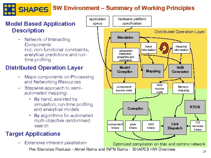
SW Environment – Summary of Working Principles Model Based Application Description application specs – Network of Interacting Components incl. non-functional constraints, analytical predictions and runtime profiling Distributed Operation Layer – Maps components on Processing and Networking Resources – Stepwise approach to semiautomated mapping: • By hand, assisted by simulation, run-time profiling and analytical models • By algorithms for automated multi-objective randomised search Target Applications – Extensive inherent parallelism hardware platform specification Distributed Operation Layer Simulator component interaction, properties and constraints trace information Model Compiler Mapping Hd. S source code component source code mapping information Hd. S Generator Memory mapping RTOS Compiler component binary glue binary Hd. S binary Link Dispatch OS services binary Optimised compilation on tiles and comms network Pier Stanislao Paolucci - Atmel Roma and INFN Roma - SHAPES HW Overview 21
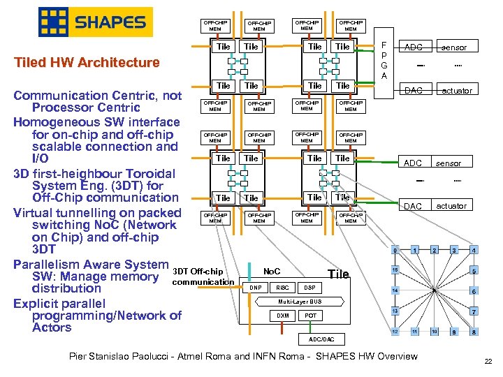
OFF-CHIP MEM Tile Tile Tiled HW Architecture Communication Centric, not Processor Centric Homogeneous SW interface for on-chip and off-chip scalable connection and Tile I/O 3 D first-heighbour Toroidal System Eng. (3 DT) for Tile Off-Chip communication Virtual tunnelling on packed switching No. C (Network on Chip) and off-chip 3 DT Parallelism Aware System 3 DT Off-chip SW: Manage memory communication distribution Explicit parallel programming/Network of Actors OFF-CHIP MEM OFF-CHIP MEM ADC sensor DAC actuator OFF-CHIP MEM F P G A OFF-CHIP MEM Tile Tile OFF-CHIP MEM No. C DNP RISC ADC sensor DAC actuator OFF-CHIP MEM Tile DSP Multi-Layer BUS DXM POT ADC/DAC Pier Stanislao Paolucci - Atmel Roma and INFN Roma - SHAPES HW Overview 22
fa2c9ba9c699d9d3cb4c6aa343fa3c3f.ppt