60cc00ab19afdd9424863ced33d5bf3a.ppt
- Количество слайдов: 34
Serial IO
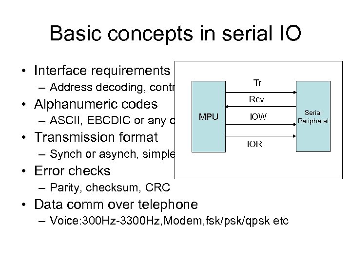
Basic concepts in serial IO • Interface requirements Tr – Address decoding, control signal generation Rcv • Alphanumeric codes MPU – ASCII, EBCDIC or any other coding • Transmission format IOW IOR Serial Peripheral – Synch or asynch, simplex/duplex, rate of transmission • Error checks – Parity, checksum, CRC • Data comm over telephone – Voice: 300 Hz-3300 Hz, Modem, fsk/psk/qpsk etc
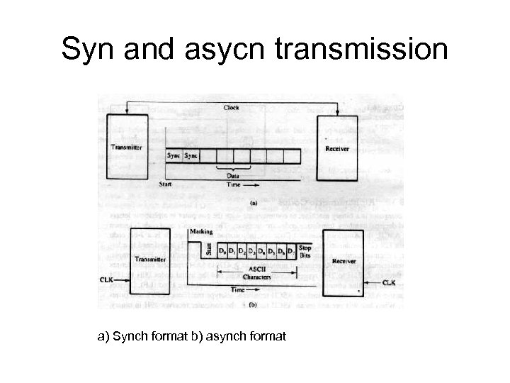
Syn and asycn transmission a) Synch format b) asynch format
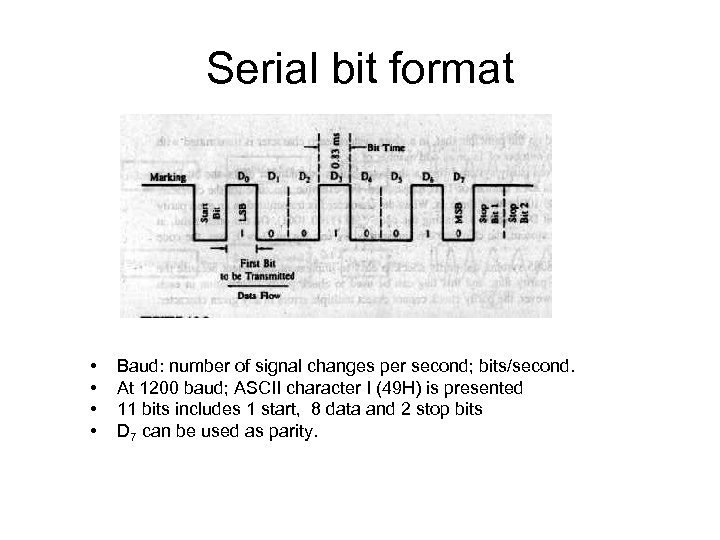
Serial bit format • • Baud: number of signal changes per second; bits/second. At 1200 baud; ASCII character I (49 H) is presented 11 bits includes 1 start, 8 data and 2 stop bits D 7 can be used as parity.
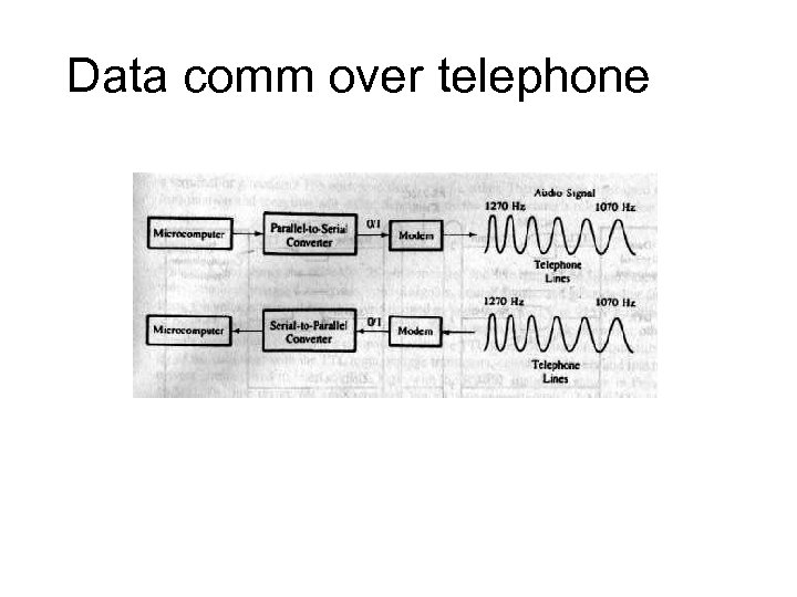
Data comm over telephone
Serial I/O standards • Commonly used to interface terminal, printer or modem. • Standard is a common specification that all the manufacturer have agreed upon. – Assigment of pin position for signal, voltage levels, speed, length of cables and mechanical specs. • Current loop – 20 m. A or 60 m. A, signals relatively noise free and suitable over a long distance. • voltage level – RS 232 C, most commonly used method – DTE, DCE
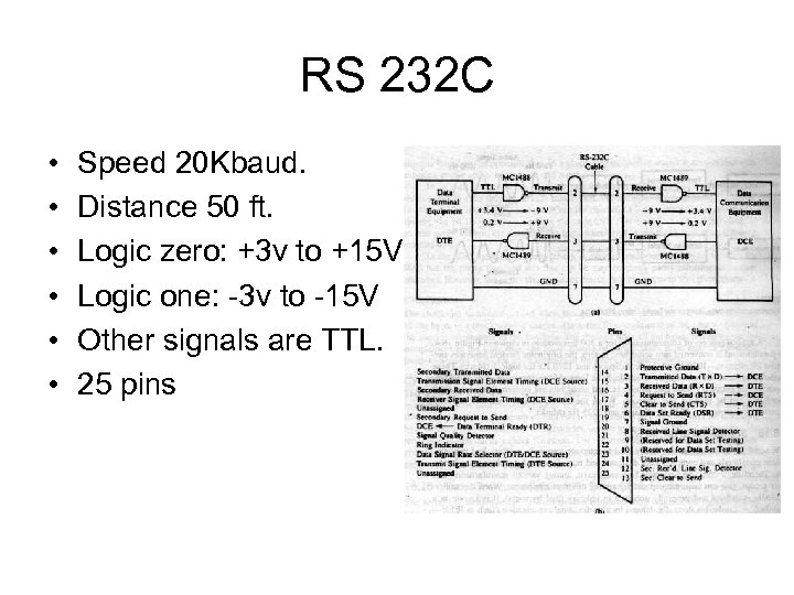
RS 232 C • • • Speed 20 Kbaud. Distance 50 ft. Logic zero: +3 v to +15 V Logic one: -3 v to -15 V Other signals are TTL. 25 pins
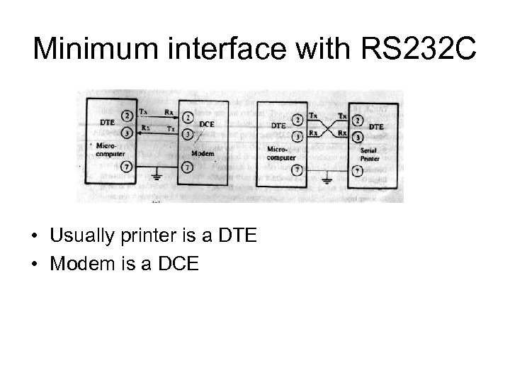
Minimum interface with RS 232 C • Usually printer is a DTE • Modem is a DCE
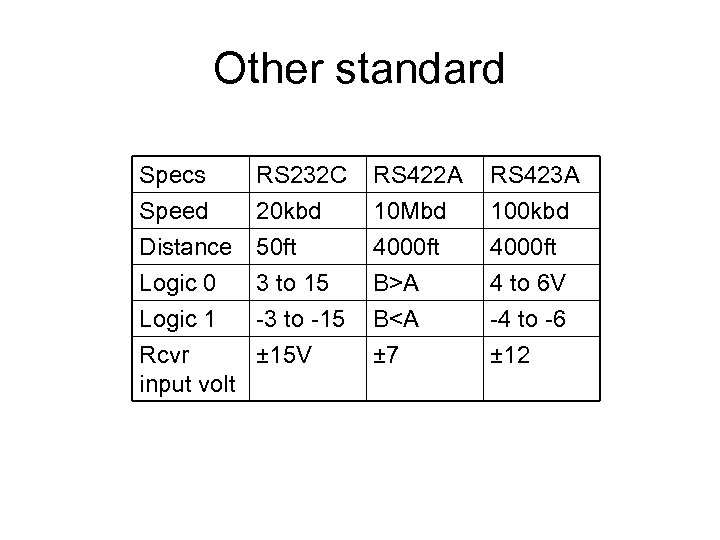
Other standard Specs Speed Distance Logic 0 RS 232 C 20 kbd 50 ft 3 to 15 Logic 1 -3 to -15 Rcvr ± 15 V input volt RS 422 A 10 Mbd 4000 ft B>A RS 423 A 100 kbd 4000 ft 4 to 6 V B<A ± 7 -4 to -6 ± 12

Software controlled Asycn serial I/O • Output start bit • Convert chara into serial stream with appr delay. • Add parity • Output stop bits.
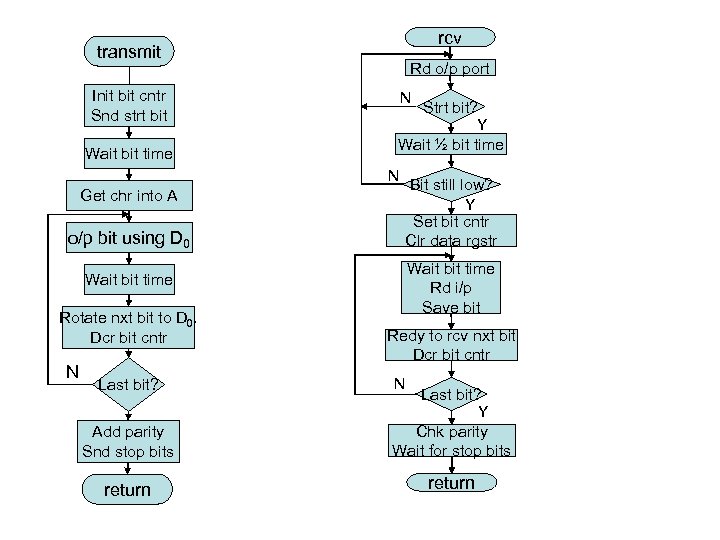
rcv transmit Init bit cntr Snd strt bit Wait bit time Rd o/p port N Strt bit? Y Wait ½ bit time N Get chr into A o/p bit using D 0 Bit still low? Y Set bit cntr Clr data rgstr Wait bit time Rd i/p Save bit Wait bit time Rotate nxt bit to D 0. Dcr bit cntr N Last bit? Redy to rcv nxt bit Dcr bit cntr N Add parity Snd stop bits Last bit? Y Chk parity Wait for stop bits return
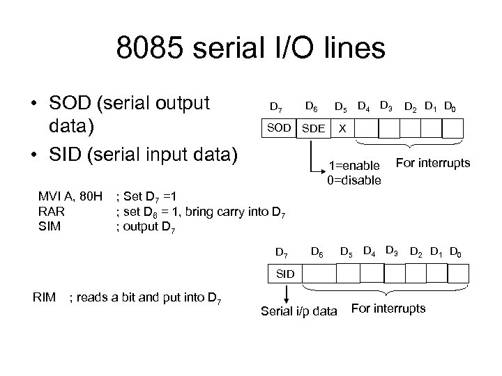
8085 serial I/O lines • SOD (serial output data) • SID (serial input data) MVI A, 80 H RAR SIM D 7 D 6 D 5 D 4 D 3 SOD SDE D 2 D 1 D 0 X 1=enable 0=disable For interrupts ; Set D 7 =1 ; set D 6 = 1, bring carry into D 7 ; output D 7 D 6 D 5 D 4 D 3 D 2 D 1 D 0 SID RIM ; reads a bit and put into D 7 Serial i/p data For interrupts
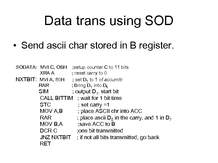
Data trans using SOD • Send ascii char stored in B register. SODATA: MVI C, OBH ; setup counter C to 11 bits XRA A ; reset carry to 0 NXTBIT: MVI A, 80 H ; set D 7 to 1 of accumltr RAR ; Bring D 7 into D 6 SIM ; output D 7; start bit CALL BITTIM ; wait for 1 bit time STC ; set carry =1 MOV A, B ; place ASCII chr into ACC RAR ; place ascii D 0 in the carry, and 1 in D 7 MOV B, A ; save ACC to B DCR C ; one bit transmitted JNZ NXTBIT ; if not all bits transmitted, go back RET

(B) = 47 H 0 1 0 0 0 1 1 1 CY D 7 D 6 D 5 D 4 D 3 D 2 D 1 D 0 XRA A MVI A, 80 H RAR 0 0 1 0 0 0 0 0 0 SIM STC MOV A, B outputs 0 as stop bit 1 0 1 0 0 0 0 0 1 0 1 RAR MOV B, A DCR C JNZ NXTBIT RAR. 1 B= C= 1 0 0 0 0 0 1 1 1 0 0 0 0 1 1 1 0 0 0 0 When ascii D 7 is sent out, register B will have all 1 s from D 0 to D 7. In the last two iterations logic 1 s are sent out as stop bits.
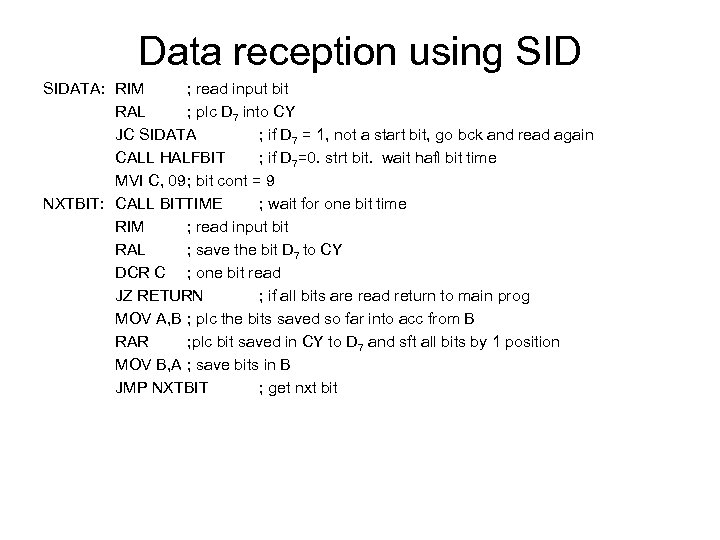
Data reception using SIDATA: RIM ; read input bit RAL ; plc D 7 into CY JC SIDATA ; if D 7 = 1, not a start bit, go bck and read again CALL HALFBIT ; if D 7=0. strt bit. wait hafl bit time MVI C, 09; bit cont = 9 NXTBIT: CALL BITTIME ; wait for one bit time RIM ; read input bit RAL ; save the bit D 7 to CY DCR C ; one bit read JZ RETURN ; if all bits are read return to main prog MOV A, B ; plc the bits saved so far into acc from B RAR ; plc bit saved in CY to D 7 and sft all bits by 1 position MOV B, A ; save bits in B JMP NXTBIT ; get nxt bit
HW controlled serial I/O • SW control has following requirements: – An input port and an output port are req for interfacing. – In transmission, MPU converts parallel data into serial bits. – In reception, MPU converts bits from serial to parallel. – Trans and rec must match the time delay. • In HW control has serial IO, all these features are incorporated in one chip, like 8251 A (USART).
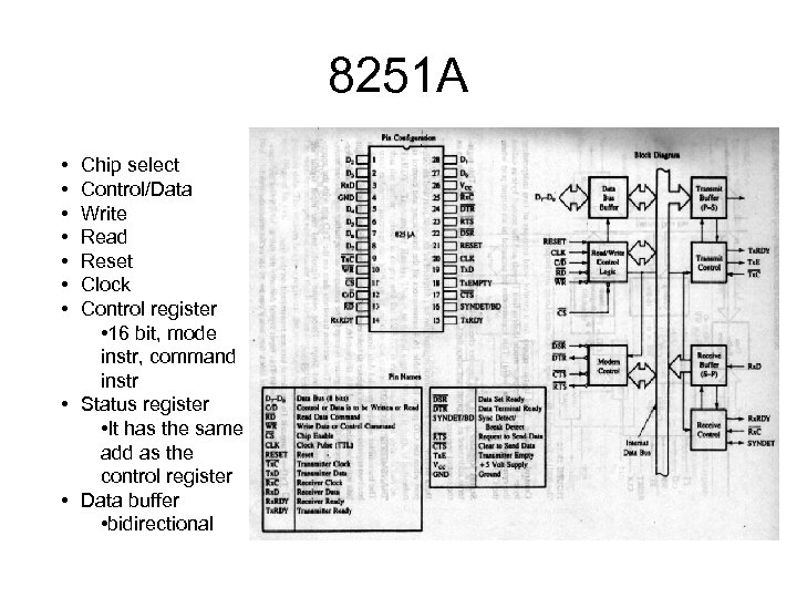
8251 A • • Chip select Control/Data Write Read Reset Clock Control register • 16 bit, mode instr, command instr • Status register • It has the same add as the control register • Data buffer • bidirectional
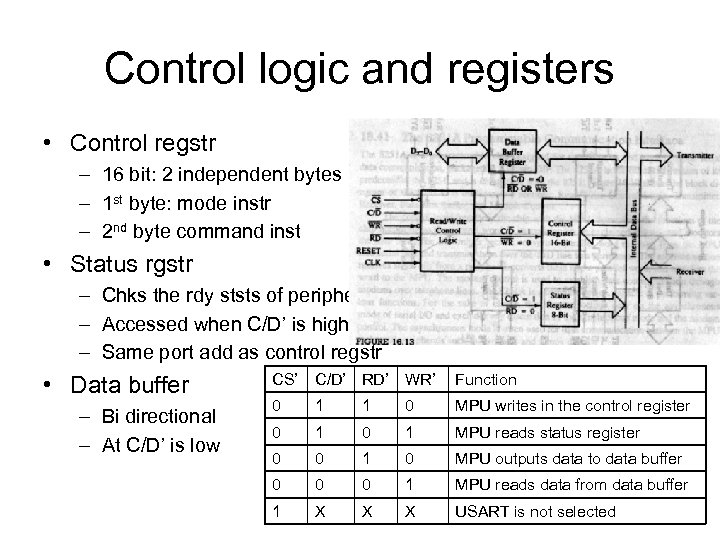
Control logic and registers • Control regstr – 16 bit: 2 independent bytes – 1 st byte: mode instr – 2 nd byte command inst • Status rgstr – Chks the rdy ststs of peripheral – Accessed when C/D’ is high – Same port add as control regstr • Data buffer – Bi directional – At C/D’ is low CS’ C/D’ RD’ WR’ Function 0 1 1 0 MPU writes in the control register 0 1 MPU reads status register 0 0 1 0 MPU outputs data to data buffer 0 0 0 1 MPU reads data from data buffer 1 X X X USART is not selected
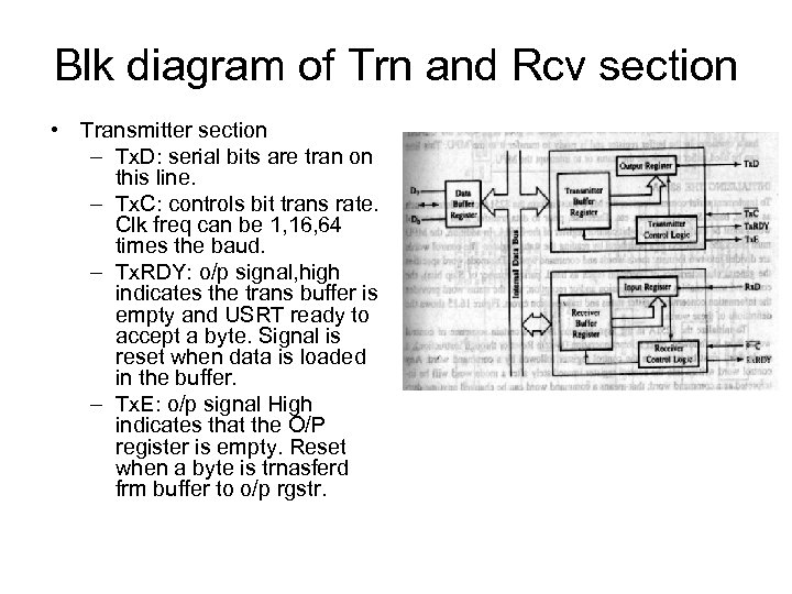
Blk diagram of Trn and Rcv section • Transmitter section – Tx. D: serial bits are tran on this line. – Tx. C: controls bit trans rate. Clk freq can be 1, 16, 64 times the baud. – Tx. RDY: o/p signal, high indicates the trans buffer is empty and USRT ready to accept a byte. Signal is reset when data is loaded in the buffer. – Tx. E: o/p signal High indicates that the O/P register is empty. Reset when a byte is trnasferd frm buffer to o/p rgstr.
Receiver section • Rx. D: bits are rcvd serially on this line • Rx. C: controls the rate at which bits are rcvd by USART. In asych mode, it can be 1, 16 or 64 times the baud. • Rx. RDY: it goes high when USART has a char on the input buffer register and ready to transfer it to MPU. Can be used either to indicate the status or to interrupt MPU.
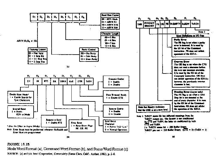
Initializing 8251 A • Mode, baud, stop bits, parity, etc. • Control word: a) mode word b) command word • After a reset operation, a mode word must be written in the control register followed by a command word. Command word can be changed at any time during operation, but mode can only be changed only after a reset operation. It can be reset using internal reset bit (D 6) in the command word.
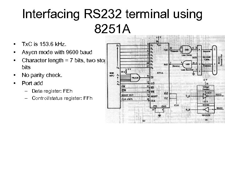
Interfacing RS 232 terminal using 8251 A • • • Tx. C is 153. 6 k. Hz. Asycn mode with 9600 baud Character length = 7 bits, two stop bits No parity check. Port add – Data register: FEh – Control/status register: FFh
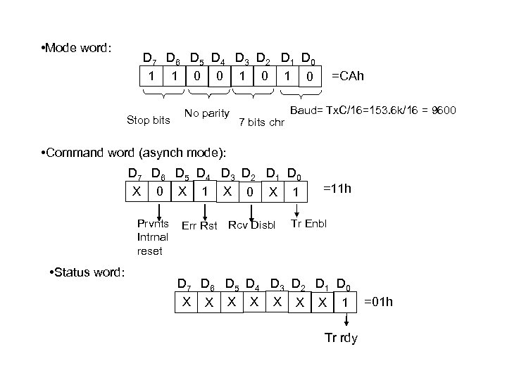
• Mode word: D 7 D 6 D 5 D 4 D 3 D 2 D 1 D 0 1 1 0 0 1 0 Stop bits No parity 7 bits chr =CAh Baud= Tx. C/16=153. 6 k/16 = 9600 • Command word (asynch mode): D 7 D 6 D 5 D 4 D 3 D 2 D 1 D 0 X 1 X 0 X 1 Prvnts Intrnal reset • Status word: Err Rst Rcv Disbl =11 h Tr Enbl D 7 D 6 D 5 D 4 D 3 D 2 D 1 D 0 X X X X 1 Tr rdy =01 h
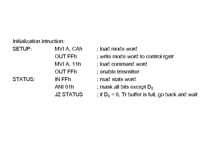
Initialization intruction: SETUP: MVI A, CAh OUT FFh MVI A, 11 h OUT FFh STATUS: IN FFh ANI 01 h JZ STATUS ; load mode word ; write mode word to control rgstr ; load command word ; enable trnsmitter ; read stats word ; mask all bits except D 0 ; if D 0 = 0, Tr buffer is full, go back and wait
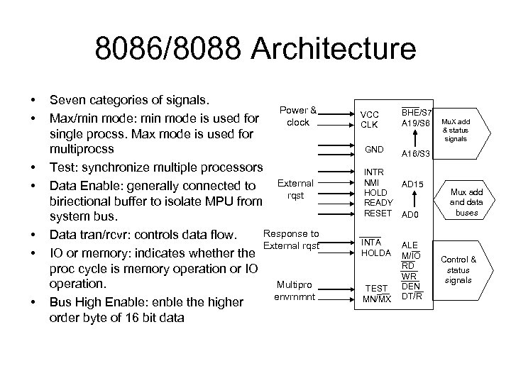
8086/8088 Architecture • • Seven categories of signals. Power & Max/min mode: min mode is used for clock single procss. Max mode is used for multiprocss Test: synchronize multiple processors External Data Enable: generally connected to rqst biriectional buffer to isolate MPU from system bus. Response to Data tran/rcvr: controls data flow. External rqst IO or memory: indicates whether the proc cycle is memory operation or IO Multipro operation. envrnmnt Bus High Enable: enble the higher order byte of 16 bit data VCC CLK GND INTR NMI HOLD READY RESET INTA HOLDA TEST MN/MX BHE/S 7 A 19/S 6 Mu. X add & status signals A 16/S 3 AD 15 AD 0 ALE M/IO RD WR DEN DT/R Mux add and data buses Control & status signals
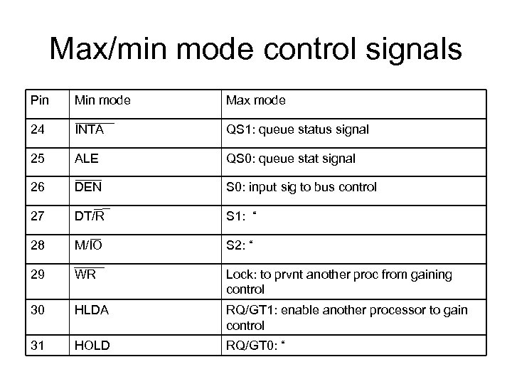
Max/min mode control signals Pin Min mode Max mode 24 INTA QS 1: queue status signal 25 ALE QS 0: queue stat signal 26 DEN S 0: input sig to bus control 27 DT/R S 1: “ 28 M/IO S 2: “ 29 WR Lock: to prvnt another proc from gaining control 30 HLDA RQ/GT 1: enable another processor to gain control 31 HOLD RQ/GT 0: “
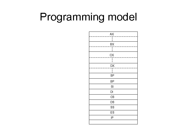
Programming model AX BX CX DX SP BP SI DI CS DS SS ES IP
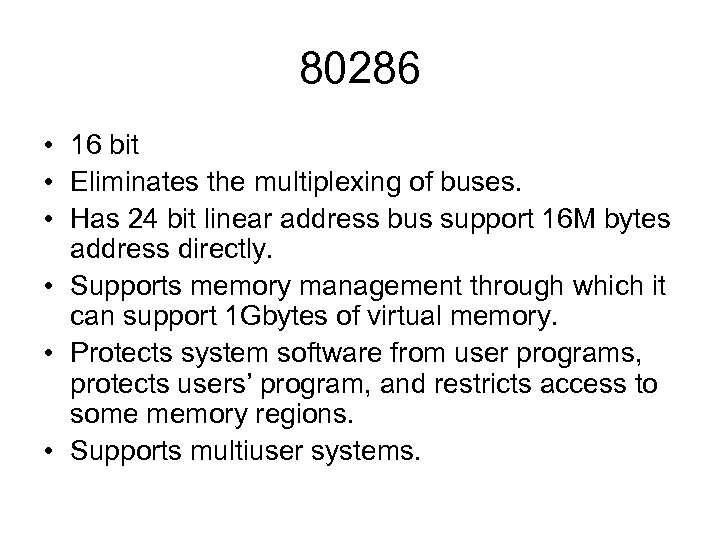
80286 • 16 bit • Eliminates the multiplexing of buses. • Has 24 bit linear address bus support 16 M bytes address directly. • Supports memory management through which it can support 1 Gbytes of virtual memory. • Protects system software from user programs, protects users’ program, and restricts access to some memory regions. • Supports multiuser systems.
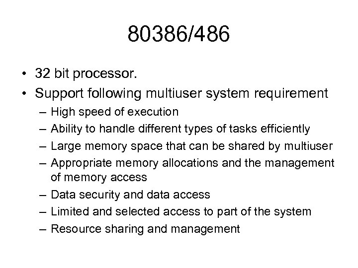
80386/486 • 32 bit processor. • Support following multiuser system requirement – – High speed of execution Ability to handle different types of tasks efficiently Large memory space that can be shared by multiuser Appropriate memory allocations and the management of memory access – Data security and data access – Limited and selected access to part of the system – Resource sharing and management
• 32 bit non-multiplexed address bus • Can address 4 G physical memory and through a memory management unit 64 (246) terabytes of virtual memory. • Two modes: real mode, and protected mode. • Execution is highly pipelined.
Functional signal groups
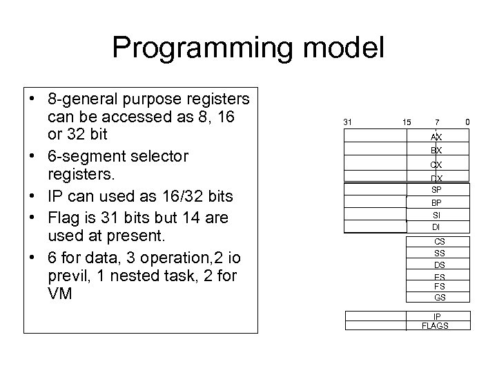
Programming model • 8 -general purpose registers can be accessed as 8, 16 or 32 bit • 6 -segment selector registers. • IP can used as 16/32 bits • Flag is 31 bits but 14 are used at present. • 6 for data, 3 operation, 2 io previl, 1 nested task, 2 for VM 31 15 7 AX BX CX DX SP BP SI DI CS SS DS ES FS GS IP FLAGS 0

60cc00ab19afdd9424863ced33d5bf3a.ppt