SEM_KZ.ppt
- Количество слайдов: 50
 SEM Scanning Electron Microscopy construction, operation and application : Prof. dr habil. ing. Włodzimierz Dudziński
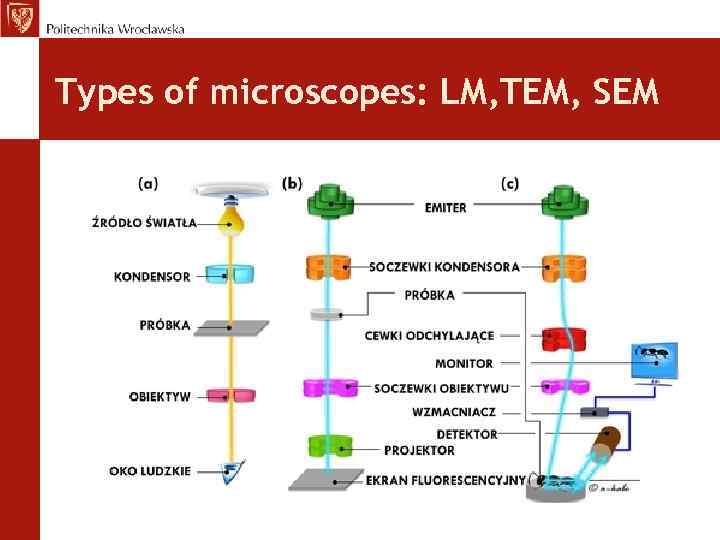 Types of microscopes: LM, TEM, SEM
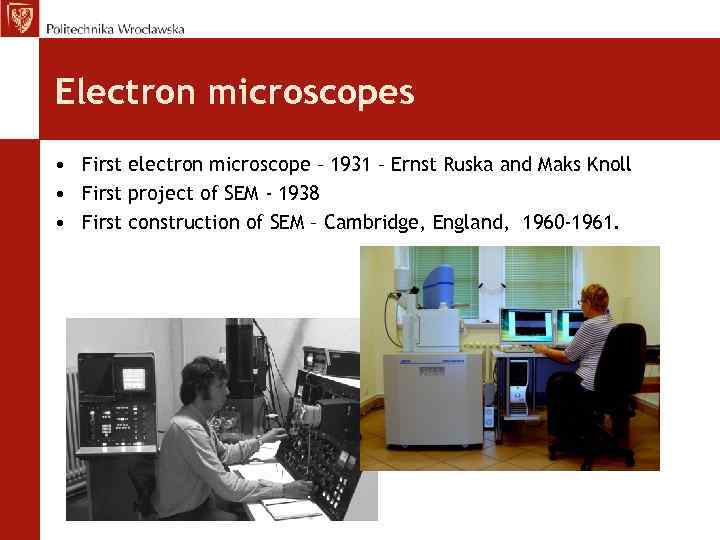 Electron microscopes • First electron microscope – 1931 – Ernst Ruska and Maks Knoll • First project of SEM - 1938 • First construction of SEM – Cambridge, England, 1960 -1961.
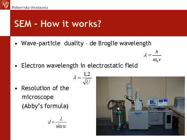 SEM – How it works? • Wave-particle duality – de Broglie wavelength • Electron wavelength in electrostatic field • Resolution of the microscope (Abby’s formula)
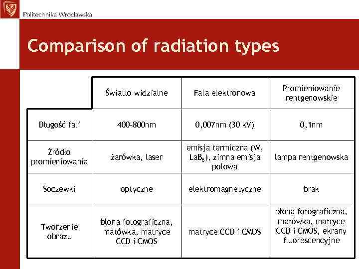 Comparison of radiation types Światło widzialne Fala elektronowa Promieniowanie rentgenowskie 400 -800 nm 0, 007 nm (30 k. V) 0, 1 nm Źródło promieniowania żarówka, laser emisja termiczna (W, La. B 6), zimna emisja polowa lampa rentgenowska Soczewki optyczne elektromagnetyczne brak Długość fali Tworzenie obrazu błona fotograficzna, matówka, matryce CCD i CMOS, ekrany fluorescencyjne
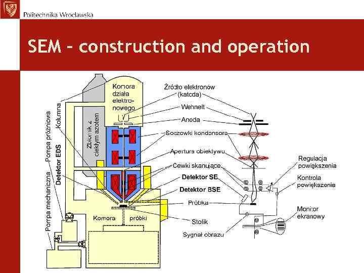 SEM – construction and operation
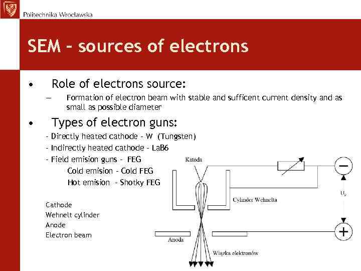 SEM – sources of electrons • Role of electrons source: — • Formation of electron beam with stable and sufficent current density and as small as possible diameter Types of electron guns: - Directly heated cathode – W (Tungsten) - Indirectly heated cathode – La. B 6 - Field emision guns - FEG Cold emision – Cold FEG Hot emision - Shotky FEG Cathode Wehnelt cylinder Anode Electron beam
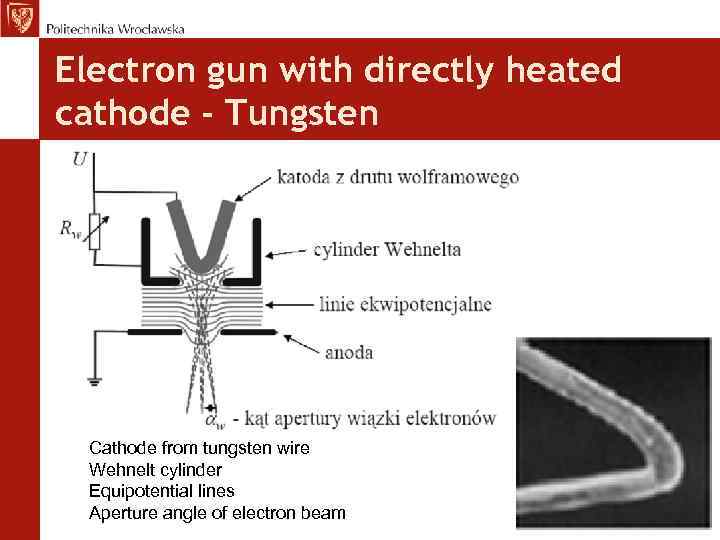 Electron gun with directly heated cathode - Tungsten Cathode from tungsten wire Wehnelt cylinder Equipotential lines Aperture angle of electron beam
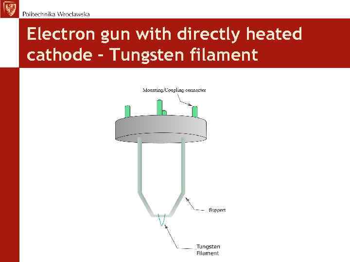 Electron gun with directly heated cathode – Tungsten filament
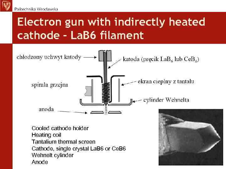 Electron gun with indirectly heated cathode – La. B 6 filament Cooled cathode holder Heating coil Tantalium thermal screen Cathode, single crystal La. B 6 or Ce. B 6 Wehnelt cylinder Anode
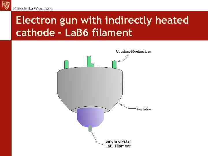 Electron gun with indirectly heated cathode – La. B 6 filament
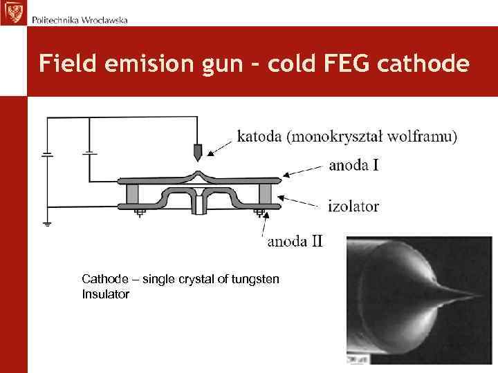 Field emision gun – cold FEG cathode Cathode – single crystal of tungsten Insulator
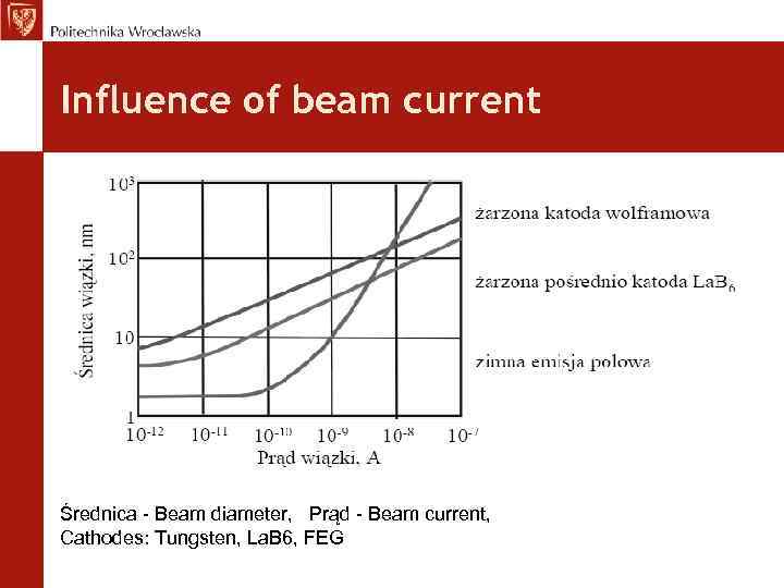 Influence of beam current Średnica - Beam diameter, Prąd - Beam current, Cathodes: Tungsten, La. B 6, FEG
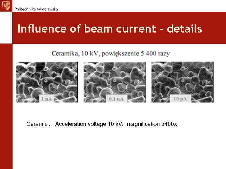 Influence of beam current - details Ceramic , Acceleration voltage 10 k. V, magnification 5400 x
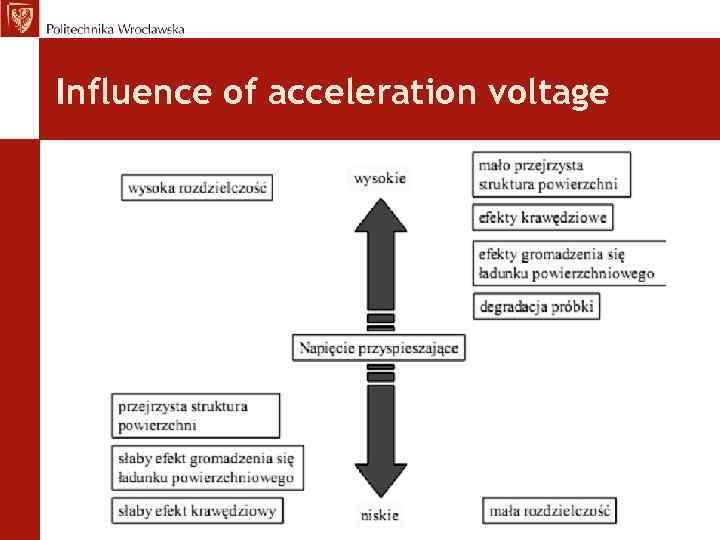 Influence of acceleration voltage
 Influence of acceleration voltage • High Acc. Voltage: high resolution, lack of surface transparency, strong effect of edge, influence of surface charge collection, strong degradation of specimen structure • Low Acc. Voltage: low resolution, transparent surface structure, low influence of surface charge collection, low effect of edge,
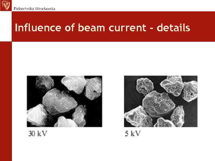 Influence of beam current - details
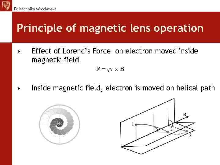 Principle of magnetic lens operation • Effect of Lorenc’s Force on electron moved inside magnetic field • Inside magnetic field, electron is moved on helical path
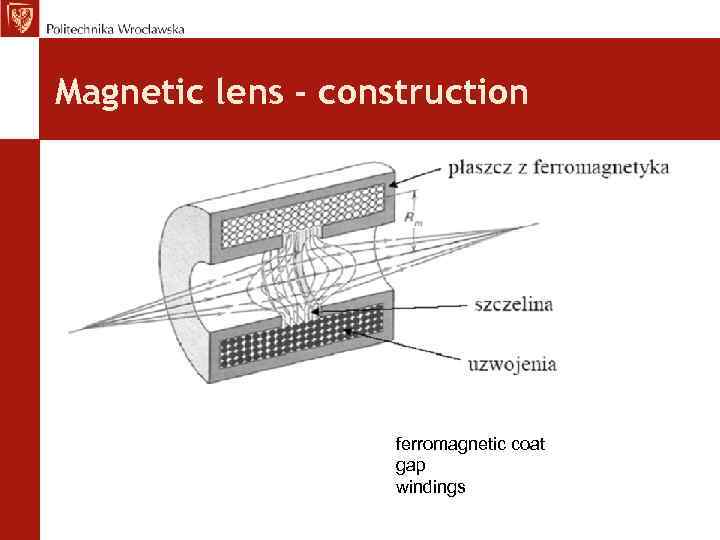 Magnetic lens - construction ferromagnetic coat gap windings
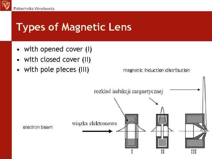 Types of Magnetic Lens • with opened cover (I) • with closed cover (II) • with pole pieces (III) electron beam magnetic induction distribution
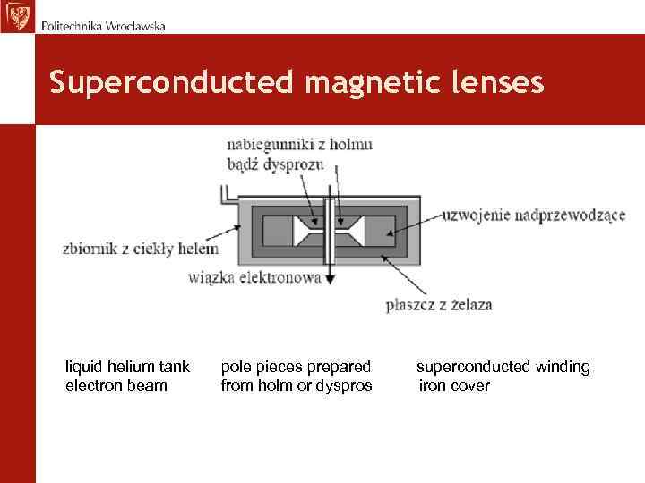 Superconducted magnetic lenses liquid helium tank pole pieces prepared superconducted winding electron beam from holm or dyspros iron cover
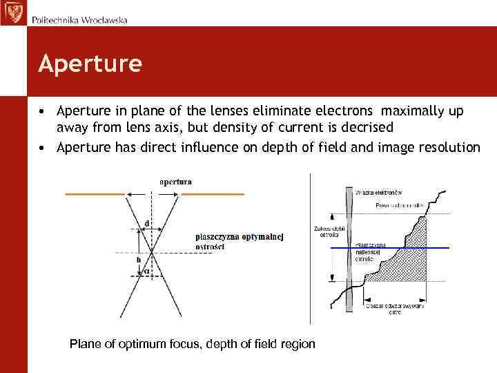 Aperture • Aperture in plane of the lenses eliminate electrons maximally up away from lens axis, but density of current is decrised • Aperture has direct influence on depth of field and image resolution Plane of optimum focus, depth of field region
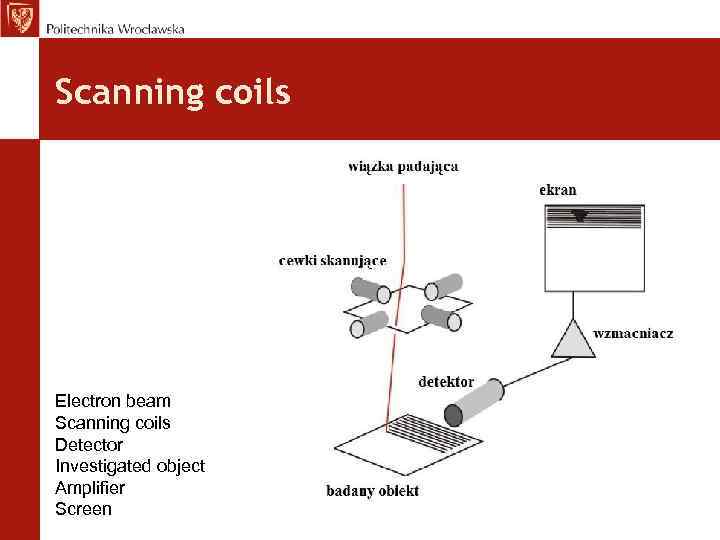 Scanning coils Electron beam Scanning coils Detector Investigated object Amplifier Screen
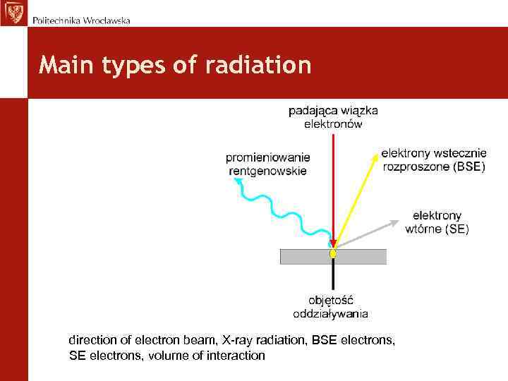 Main types of radiation direction of electron beam, X-ray radiation, BSE electrons, volume of interaction
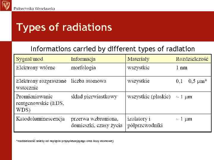 Types of radiations Informations carried by different types of radiation *rozdzielczość zależy od napięcia przyspieszającego oraz liczy atomowej
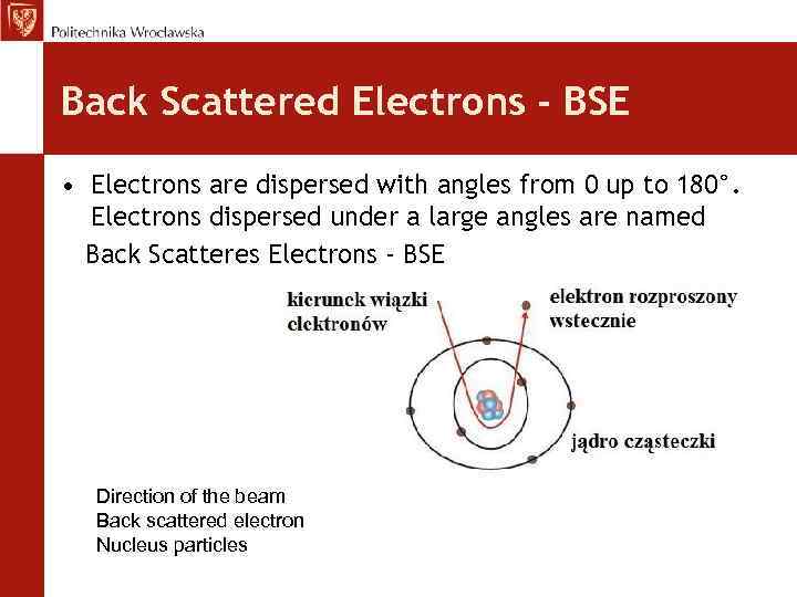 Back Scattered Electrons - BSE • Electrons are dispersed with angles from 0 up to 180°. Electrons dispersed under a large angles are named Back Scatteres Electrons - BSE Direction of the beam Back scattered electron Nucleus particles
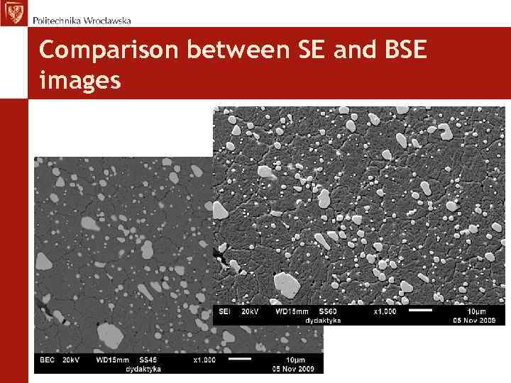 Comparison between SE and BSE images
 Absorbed Electrons - AE • Regions richer with heavy elements looks like dark • Regions contained light elements looks like brighter
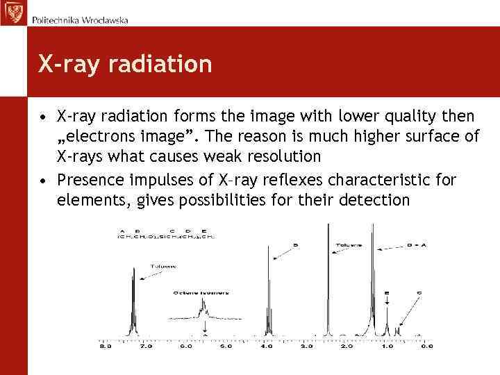 X-ray radiation • X-ray radiation forms the image with lower quality then „electrons image”. The reason is much higher surface of X-rays what causes weak resolution • Presence impulses of X–ray reflexes characteristic for elements, gives possibilities for their detection
 Cathodoluminescence • Emission of the visible light emited by solids/rocks caused by electron beam excitation • With the aid of this phenomen it is possible to make observations of rocks properties which are not visible under ordinary petrographic/polarised microscope
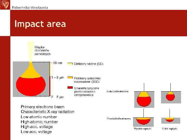 Impact area Primary electrons beam Characteristic X-ray radiation Low atomic number High acc. voltage Low acc. voltage
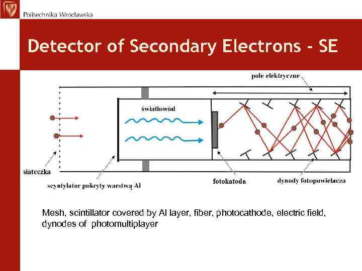 Detector of Secondary Electrons - SE Mesh, scintillator covered by Al layer, fiber, photocathode, electric field, dynodes of photomultiplayer
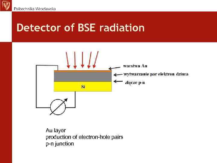 Detector of BSE radiation Au layer production of electron-hole pairs p-n junction
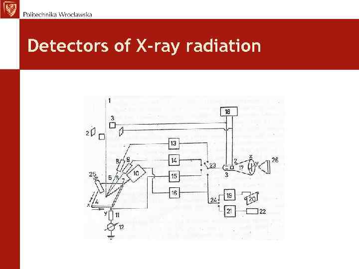 Detectors of X-ray radiation
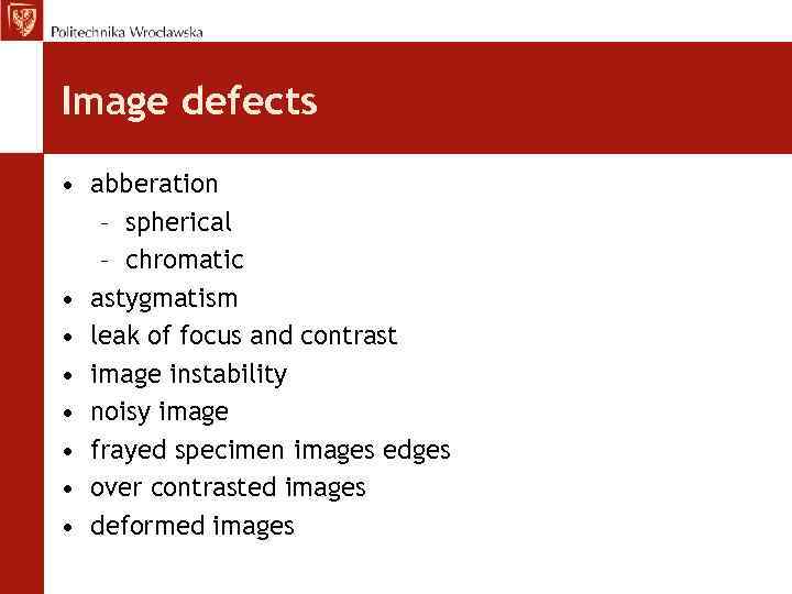 Image defects • abberation – spherical – chromatic • astygmatism • leak of focus and contrast • image instability • noisy image • frayed specimen images edges • over contrasted images • deformed images
 Main possibilities of SEM microscope • Resolution much higher then application by light microscope (up to 5 nm with magnification 105 times) • Possibilities investigation of specimen with very different topography • From the reason of small angle aperture, depth of focus it is up to 300 times higher compared with light microscopes working with identical magnification • Possibility to install detectors EDS or WDS for chemical analyse or EBSD detectors for crystallographic analyse
 Main types of materials investigated by SEM methods • Insulators - materials non conducted electrical current • Conductors – materials conducted electrical current • Semi conductors
 Rules of specimens preparation for SEM investigation • Adjustement of specimen size corresponding to the microscope holder/or specimen table dimension • Cleaning of specimen surface/ultrasonic washing • Covering of non conductive specimen surface, by vaporized or sputered elements like: C, Au, Pt, Cu.
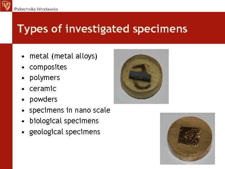 Types of investigated specimens • • metal (metal alloys) composites polymers ceramic powders specimens in nano scale biological specimens geological specimens
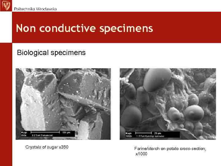 Non conductive specimens Biological specimens Crystals of sugar x 350 Farine/storch on potato cross-section, x 1000
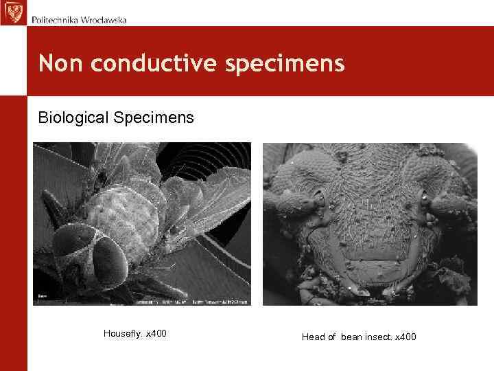 Non conductive specimens Biological Specimens Housefly. x 400 Head of bean insect. x 400
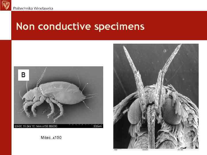 Non conductive specimens Mites. x 150
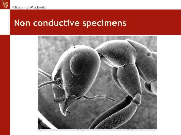 Non conductive specimens
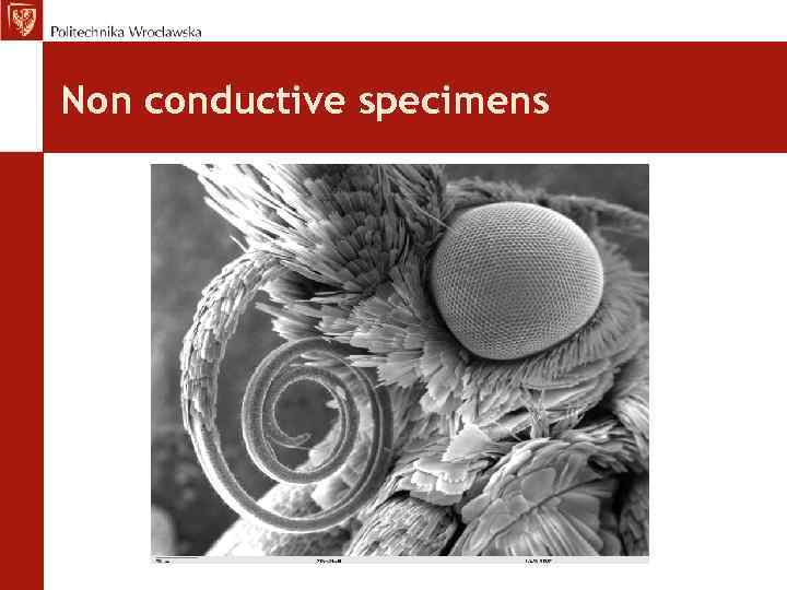 Non conductive specimens
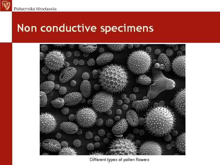 Non conductive specimens Different types of pollen flowers
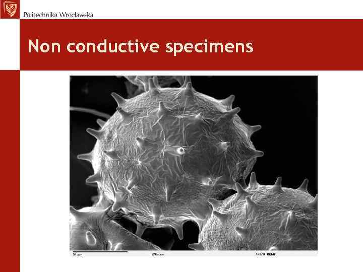 Non conductive specimens
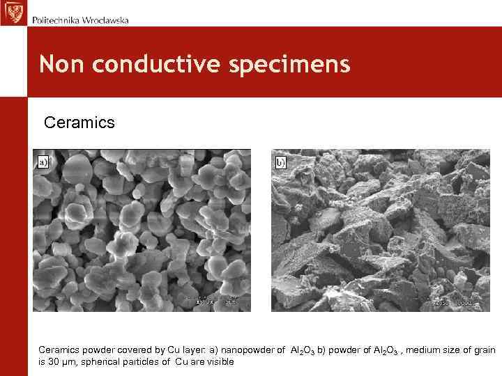 Non conductive specimens Ceramics powder covered by Cu layer: a) nanopowder of Al 2 O 3 b) powder of Al 2 O 3 , medium size of grain is 30 μm, spherical particles of Cu are visible
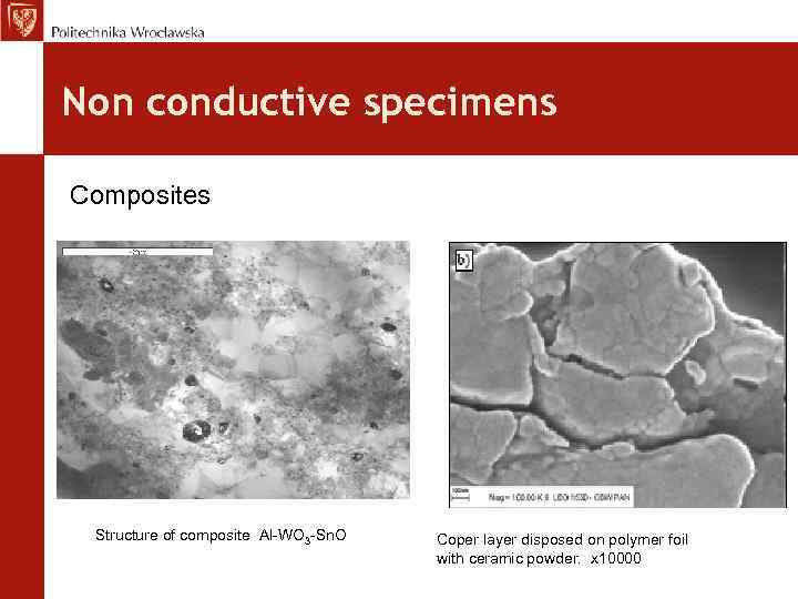 Non conductive specimens Composites Structure of composite Al-WO 3 -Sn. O Coper layer disposed on polymer foil with ceramic powder. x 10000
 Bibliography • • • Reimer – Scaning electron microscopy http: //www. kgmip. wnoz. us. edu. pl/ http: //www. sgml. pwr. wroc. pl/ http: //www. biolog. pl/ http: //www. chemia. uj. edu. pl/ http: //pl. wikipedia. org/wiki/
 Thank You for Your attention


