806827b458c6940435a53206e714ea7a.ppt
- Количество слайдов: 37
SEM Magnification Calibration
Magnification Errors • Proper calibration of the SEM scans (magnification) is primary to metrology. • SEM Magnification requires calibration – Standards needed • Instrument has inherent systematic problems – k. V compensation – Working distance compensation • Operator Errors – Working distance
Magnification Calibration • SEM magnification calibration is generally based on the measurement of the pitch (displacement) between two structures. – Pitch will be discussed later • All traceable SEM magnification calibration is based on the measurement of a pitch.
SEM Magnification Calibration • Procedures vary with instrument manufacturer. • All require user supplied calibration sample. • Most common sample for laboratory instruments is a copper grid. • NIST SRM 484 is a sample with accurate pitch dimensions for SEM magnification calibration.
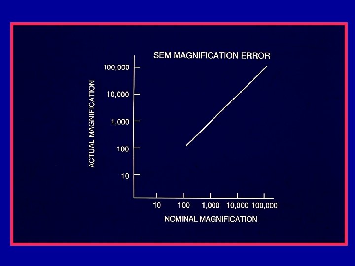
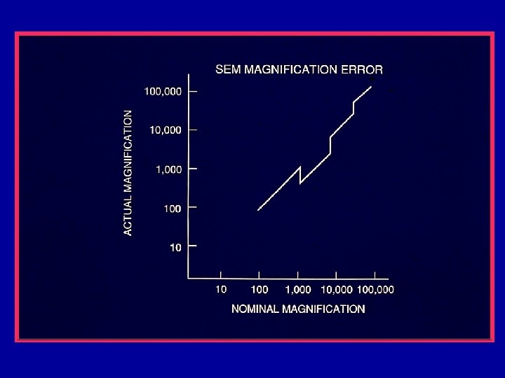
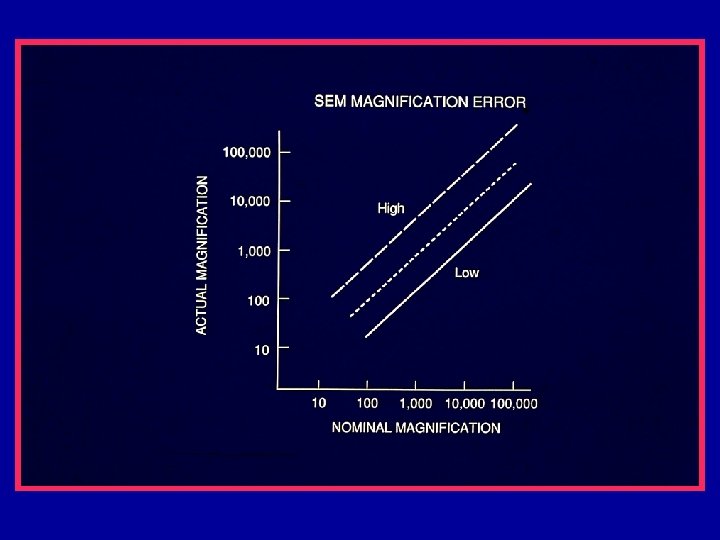

SEM Instrumentation • Vast array of instruments in the field. • Performance and capabilities vary substantially. – lab instruments – production line instruments • Universally useful NIST sample preferred because of time and cost involved.
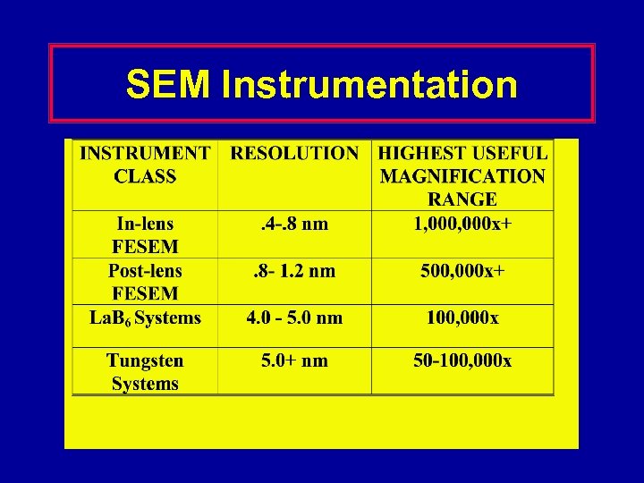
SEM Instrumentation

Independent of Accelerating Voltage
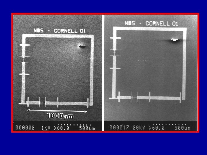
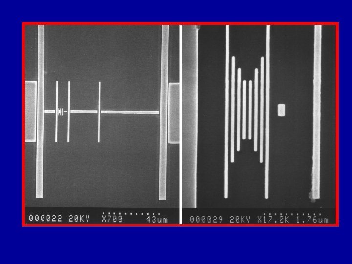
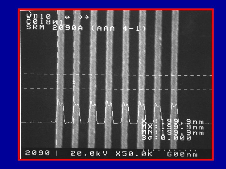

Calibration Based on Pitch
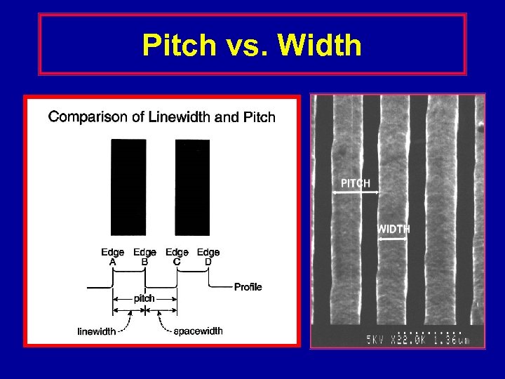
Pitch vs. Width
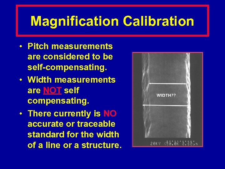
Magnification Calibration • Pitch measurements are considered to be self-compensating. • Width measurements are NOT self compensating. • There currently is NO accurate or traceable standard for the width of a line or a structure.
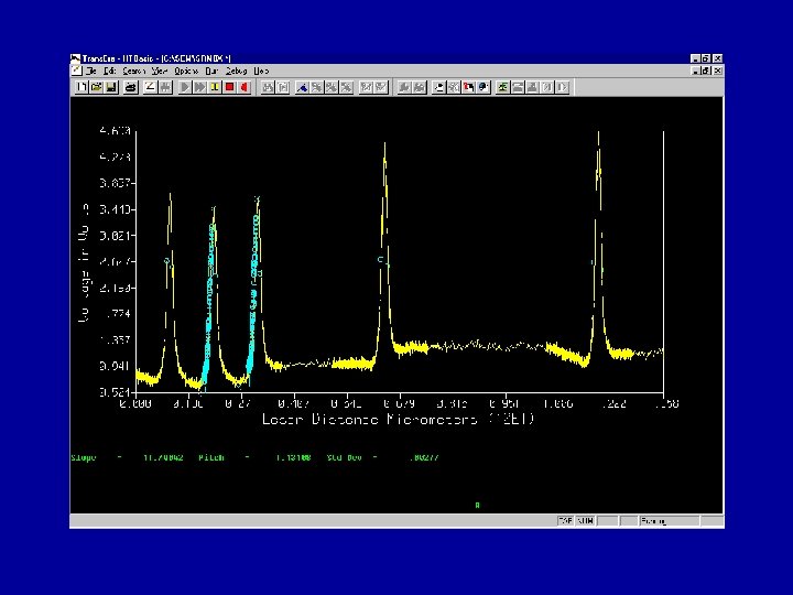
Pitch Measurements • Electron beam modeling is not needed for pitch measurements or calculations based on pitch • Pitch Measurements are self compensating • But - the rules must be followed. – The edges measured must be the same

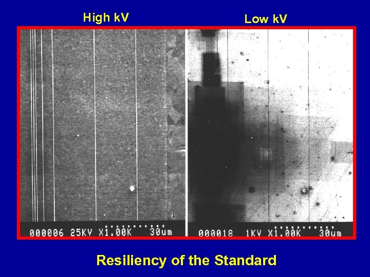
High k. V Low k. V Resiliency of the Standard
SEM Magnification Calibration Samples • Instrument Manufacturer – Hitachi – Biorad • In-house standards – Company standards laboratory • NIST Traceable Standards
NIST Traceable Standards • SRM 484 – Traditional SEM magnification standard • RM 8090 • RM 8820 • Reference material currently available • ~$400 -500 • MRS-2/MRS-3 (Geller Micro. Analytical) • VLSI Standards
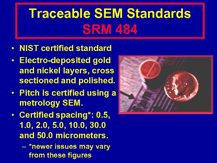
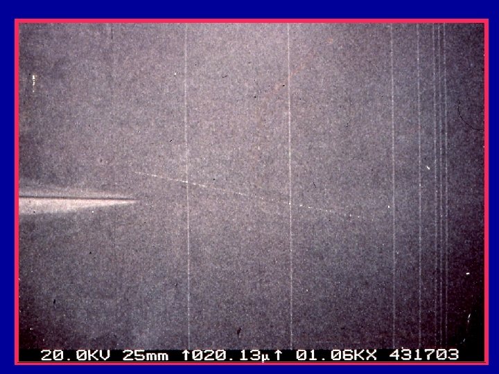
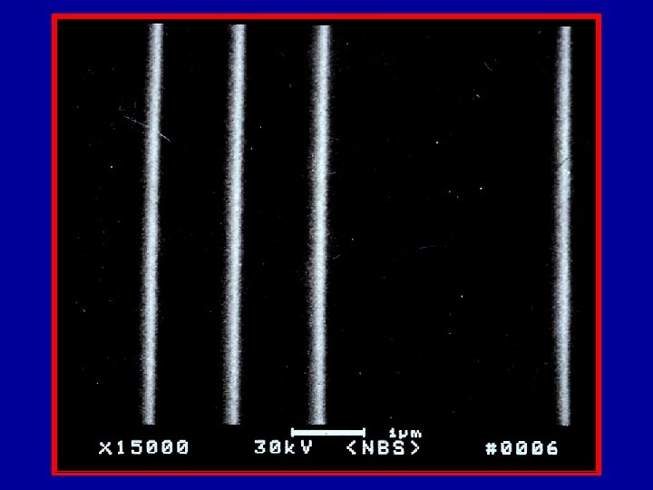
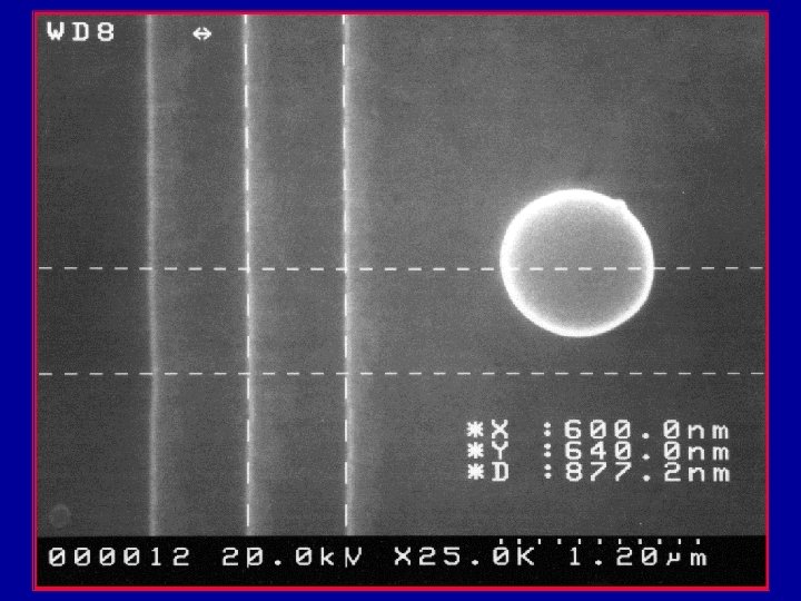
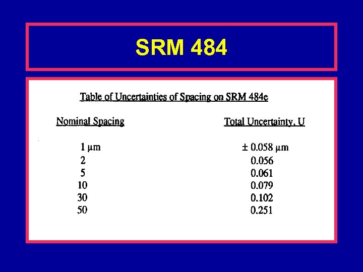
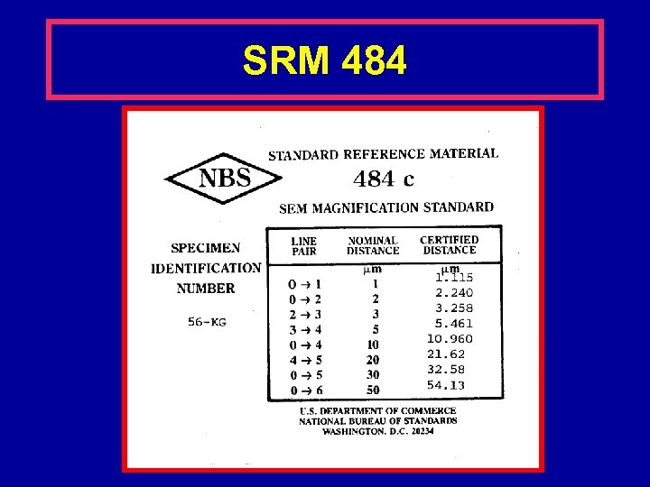
Traceable SEM Standards SRM 484 • NIST certified standard • Electro-deposited gold and nickel layers, cross sectioned and polished. • Pitch is certified using a metrology SEM. • Certified spacing*: 0. 5, 1. 0, 2. 0, 5. 0, 10. 0, 30. 0 and 50. 0 micrometers. – *newer issues may vary from these figures
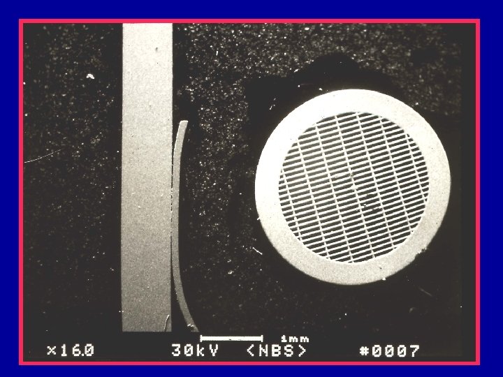
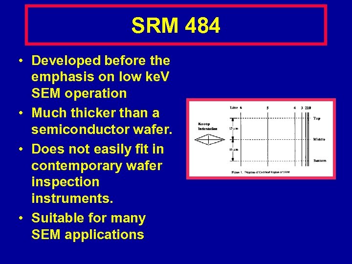
SRM 484 • Developed before the emphasis on low ke. V SEM operation • Much thicker than a semiconductor wafer. • Does not easily fit in contemporary wafer inspection instruments. • Suitable for many SEM applications
SRM 484
SRM 484
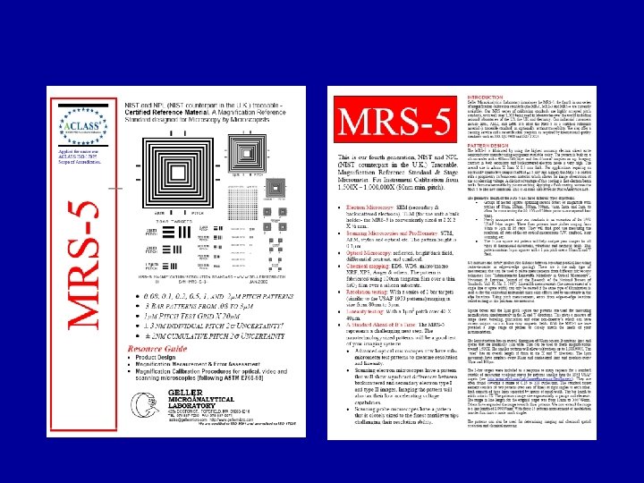
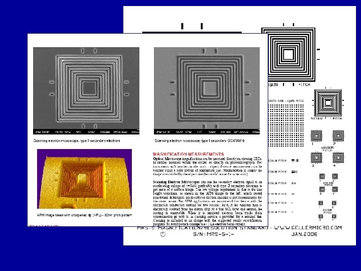
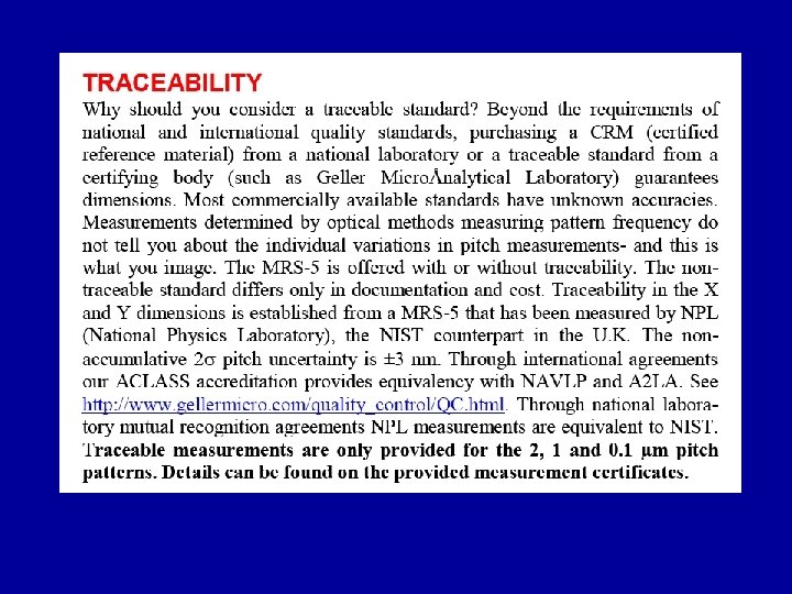
Traceable SEM Standards MRS-5 • NIST traceable standard commercially available. • Accessory structures for distortion measurements and astigmatism correction are present.
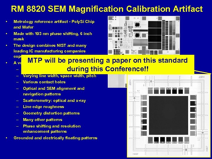
RM 8820 SEM Magnification Calibration Artifact • Metrology reference artifact - Poly. Si Chip and Wafer • Made with 193 nm phase shifting, 6 inch mask • The design combines NIST and many leading IC manufacturing companies experts’ dimensional metrology patterns • A very large variety of patterns: – MTP will be presenting a paper on this standard Isolated and dense lines and spaces during this Conference!! – Varying line width, space width, pitch – Various contact holes – Optical and SEM alignment and navigation patterns – Scatterometry: optical and x-ray – Line edge roughness – Geometry distortion patterns – Many other patterns – Phase shifting and resolution enhancement patterns • Grounded and electrically floating patterns
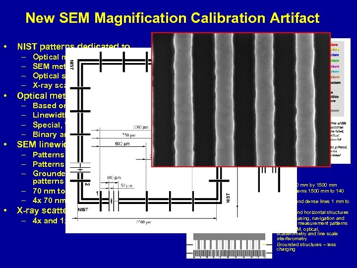
New SEM Magnification Calibration Artifact SEM pitch calibration metrology patterns • NIST patterns dedicated to – – • Optical metrology section – – • Optical metrology SEM metrology Optical scatterometry X-ray scatterometry Based on the NIST SRM 2059 design Linewidth model comparison features Special, “noisy” scatterometry patterns Binary and phase shifting patterns SEM linewidth metrology – Patterns sized for mask measurements – Patterns sized for wafer measurements – Grounded and electrically floating patterns – 70 nm to 1000 nm patterns – 4 x 70 nm to 4 x 1000 nm patterns • X-ray scatterometry – 4 x and 1 x dense structures • • Size 1500 mm by 1500 mm Pitch patterns 1500 mm to 140 nm Isolated and dense lines 1 mm to 70 nm Vertical and horizontal structures Beam focusing, navigation and distortion measurement patterns SEM, SPM, optical, scatterometry and line scale interferometry Grounded structures – less charging
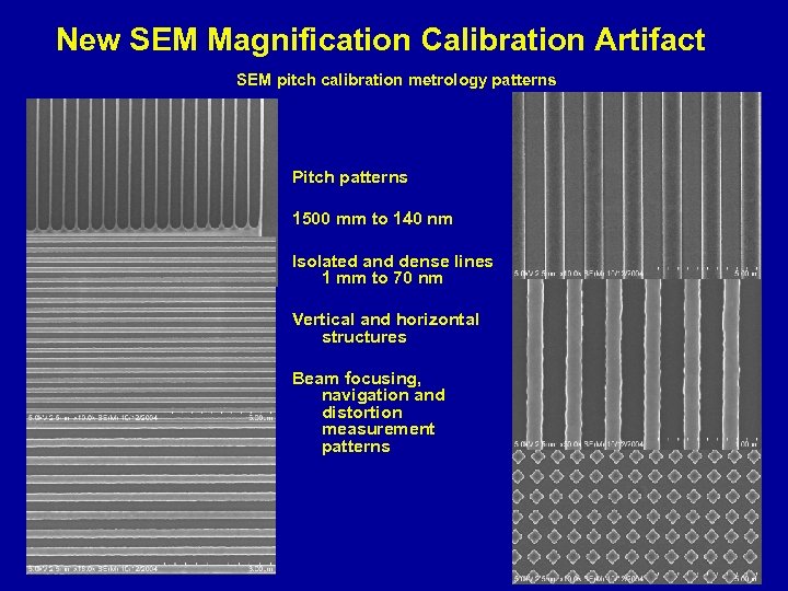
New SEM Magnification Calibration Artifact SEM pitch calibration metrology patterns Pitch patterns 1500 mm to 140 nm Isolated and dense lines 1 mm to 70 nm Vertical and horizontal structures Beam focusing, navigation and distortion measurement patterns
806827b458c6940435a53206e714ea7a.ppt