srs #1 nanodis..pptx
- Количество слайдов: 16
 SCANNING ELECTRON MICROSCOPE
 A scanning electron microscope (SEM) is a type of electron microscope that produces images of a sample by scanning it with a focused beam of electrons. The electrons interact with atoms in the sample, producing various signals that can be detected and that contain information about the sample's surface topography and composition. The electron beam is generally scanned in a raster scan pattern, and the beam's position is combined with the detected signal to produce an image. SEM can achieve resolution better than 1 nanometer. Specimens can be observed in high vacuum, in low vacuum, in wet conditions (in environmental SEM), and at a wide range of cryogenic or elevated temperatures.
 HISTORY An account of the early history of SEM has been presented by Mc. Mullan. Although Max Knoll produced a photo with a 50 mm object-field-width showing channeling contrast by the use of an electron beam scanner, it was Manfred von Ardenne who in 1937 invented a true microscope with high magnification by scanning a very small raster with a demagnified and finely focused electron beam. Ardenne applied the scanning principle not only to achieve magnification but also to purposefully eliminate the chromatic aberration otherwise inherent in the electron microscope. Further work was reported by Zworykin's group, followed by the Cambridge groups in the 1950 s and early 1960 s headed by Charles Oatley, all of which finally led to the marketing of the first commercial instrument by. Cambridge Scientific Instrument Company as the "Stereoscan" in 1965
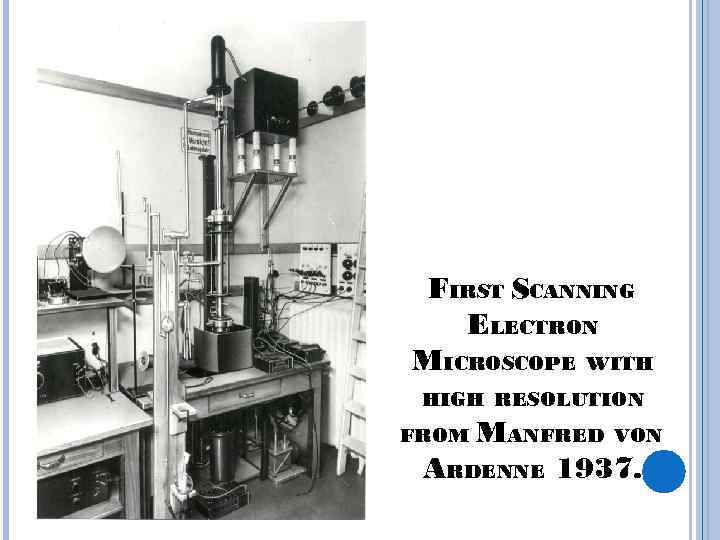 FIRST SCANNING ELECTRON MICROSCOPE WITH HIGH RESOLUTION MANFRED VON ARDENNE 1937. FROM
 PRINCIPLES AND CAPACITIES The types of signals produced by a SEM include secondary electrons (SE), back-scattered electrons (BSE), characteristic Xrays, light (cathodoluminescence) (CL), specimen current and transmitted electrons. Secondary electron detectors are standard equipment in all SEMs, but it is rare that a single machine would have detectors for all possible signals. The signals result from interactions of the electron beam with atoms at or near the surface of the sample. In the most common or standard detection mode, secondary electron imaging or SEI, the SEM can produce very high-resolution images of a sample surface, revealing details less than 1 nm in size. Due to the very narrow electron beam, SEM micrographs have a large depth of field yielding a characteristic three-dimensional appearance useful for understanding the surface structure of a sample. A wide range of magnifications is possible, from about 10 times (about equivalent to that of a powerful hand-lens) to more than 500, 000 times, about 250 times the magnification limit of the best light microscopes.
 PRINCIPLES AND CAPACITIES Back-scattered electrons (BSE) are beam electrons that are reflected from the sample by elastic scattering. BSE are often used in analytical SEM along with the spectra made from the characteristic X-rays, because the intensity of the BSE signal is strongly related to the atomic number (Z) of the specimen. BSE images can provide information about the distribution of different elements in the sample. For the same reason, BSE imaging can image colloidal gold immuno-labels of 5 or 10 nm diameter, which would otherwise be difficult or impossible to detect in secondary electron images in biological specimens. Characteristic X-rays are emitted when the electron beam removes an inner shell electron from the sample, causing a higher-energy electron to fill the shell and release energy. These characteristic X-rays are used to identify the composition and measure the abundance of elements in the sample.
 THESE POLLEN GRAINS TAKEN ON AN SEM SHOW THE CHARACTERISTIC DEPTH OF FIELD OF SEM MICROGRAPHS.
 SAMPLE PREPARATION All samples must be of an appropriate size to fit in the specimen chamber and are generally mounted rigidly on a specimen holder called a specimen stub. Several models of SEM can examine any part of a 6 -inch (15 cm) semiconductor wafer, and some can tilt an object of that size to 45°. For conventional imaging in the SEM, specimens must be electrically conductive, at least at the surface, and electrically grounded to prevent the accumulation of electrostatic charge at the surface. Metal objects require little special preparation for SEM except for cleaning and mounting on a specimen stub. Nonconductive specimens tend to charge when scanned by the electron beam, and especially in secondary electron imaging mode, this causes scanning faults and other image artifacts. They are therefore usually coated with an ultrathin coating of electrically conducting material, deposited on the sample either by low-vacuum sputter coating or by high-vacuum evaporation
 SAMPLE PREPARATION Conductive materials in current use for specimen coating include gold, gold/palladium alloy, platinum, osmium, iridium, tungsten, chromium, and graphite. Additionally, coating with heavy metals may increase signal/noise ratio for samples of low atomic number (Z). The improvement arises because secondary electron emission for high -Z materials is enhanced. An alternative to coating for some biological samples is to increase the bulk conductivity of the material by impregnation with osmium using variants of the OTO staining method (O-osmium, T-thiocarbohydrazide, Oosmium). Nonconducting specimens may be imaged uncoated using environmental SEM (ESEM) or low-voltage mode of SEM operation. Environmental SEM instruments place the specimen in a relatively high-pressure chamber where the working distance is short and the electron optical column is differentially pumped to keep vacuum adequately low at the electron gun.
 SAMPLE PREPARATION The high-pressure region around the sample in the ESEM neutralizes charge and provides an amplification of the secondary electron signal. Low-voltage SEM is typically conducted in an FEG-SEM because the field emission guns (FEG) is capable of producing high primary electron brightness and small spot size even at low accelerating potentials. Operating conditions to prevent charging of non-conductive specimens must be adjusted such that the incoming beam current was equal to sum of outcoming secondary and backscattered electrons currents. It usually occurs at accelerating voltages of 0. 3– 4 k. V. Embedding in a resin with further polishing to a mirror-like finish can be used for both biological and materials specimens when imaging in backscattered electrons or when doing quantitative X-ray microanalysis. The main preparation techniques are not required in the environmental SEM outlined below, but some biological specimens can benefit from fixation.
 SCANNING PROCESS AND IMAGE FORMATION In a typical SEM, an electron beam is thermionically emitted from an electron gun fitted with a tungsten filament cathode. Tungsten is normally used in thermionic electron guns because it has the highest melting point and lowest vapour pressure of all metals, thereby allowing it to be heated for electron emission, and because of its low cost. Other types of electron emitters include lanthanum hexaboride (La. B 6) cathodes, which can be used in a standard tungsten filament SEM if the vacuum system is upgraded and FEG, which may be of the cold-cathode type using tungsten single crystal emitters or thermally assisted Schottky type, using emitters of zirconium oxide. The electron beam, which typically has an energy ranging from 0. 2 ke. V to 40 ke. V, is focused by one or two condenser lenses to a spot about 0. 4 nm to 5 nm in diameter.
 SCANNING PROCESS AND IMAGE FORMATION The beam passes through pairs of scanning coils or pairs of deflector plates in the electron column, typically in the final lens, which deflect the beam in the x and y axes so that it scans in a raster fashion over a rectangular area of the sample surface. When the primary electron beam interacts with the sample, the electrons lose energy by repeated random scattering and absorption within a teardrop-shaped volume of the specimen known as the interaction volume, which extends from less than 100 nm to approximately 5 µm into the surface. The size of the interaction volume depends on the electron's landing energy, the atomic number of the specimen and the specimen's density. The energy exchange between the electron beam and the sample results in the reflection of high-energy electrons by elastic scattering, emission of secondary electrons by inelastic scattering and the emission of electromagnetic radiation, each of which can be detected by specialized detectors.
 SCANNING PROCESS AND IMAGE FORMATION The beam current absorbed by the specimen can also be detected and used to create images of the distribution of specimen current. Electronic amplifiers of various types are used to amplify the signals, which are displayed as variations in brightness on a computer monitor (or, for vintage models, on a cathode ray tube). Each pixel of computer videomemory is synchronized with the position of the beam on the specimen in the microscope, and the resulting image is therefore a distribution map of the intensity of the signal being emitted from the scanned area of the specimen. In older microscopes image may be captured by photography from a high-resolution cathode ray tube, but in modern machines image is saved to a computer data storage.
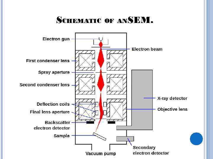 SCHEMATIC OF ANSEM.
 SEM ADVANTAGES Advantages of a Scanning Electron Microscope include its wide-array of applications, the detailed three-dimensional and topographical imaging and the versatile information garnered from different detectors. SEMs are also easy to operate with the proper training and advances in computer technology and associated software make operation user-friendly. This instrument works fast, often completing SEI, BSE and EDS analyses in less than five minutes. In addition, the technological advances in modern SEMs allow for the generation of data in digital form. Although all samples must be prepared before placed in the vacuum chamber, most SEM samples require minimal preparation actions.
 SEM DISADVANTAGES The disadvantages of a Scanning Electron Microscope start with the size and cost. SEMs are expensive, large and must be housed in an area free of any possible electric, magnetic or vibration interference. Maintenance involves keeping a steady voltage, currents to electromagnetic coils and circulation of cool water. Special training is required to operate an SEM as well as prepare samples. The preparation of samples can result in artifacts. The negative impact can be minimized with knowledgeable experience researchers being able to identify artifacts from actual data as well as preparation skill. There is no absolute way to eliminate or identify all potential artifacts. In addition, SEMs are limited to solid, inorganic samples small enough to fit inside the vacuum chamber that can handle moderate vacuum pressure. Finally, SEMs carry a small risk of radiation exposure associated with the electrons that scatter from beneath the sample surface. The sample chamber is designed to prevent any electrical and magnetic interference, which should eliminate the chance of radiation escaping the chamber. Even though the risk is minimal, SEM operators and researchers are advised to observe safety precautions.


