39aab218757f05a6bf5f0ac037266d4d.ppt
- Количество слайдов: 31
 RTU 1 A-5 A 25 GHz 3. 3 d. B NF Low Noise Amplifier based upon Slow Wave Transmission Lines and the 0. 18 μm CMOS Technology A. Sayag(1), S. Levin(2), D. Regev(2), D. Zfira(2), S. Shapira(2), D. Goren(3) and D. Ritter(1) Department of Electrical Engineering, Technion, Haifa, Israel (2) Tower Semiconductors inc. , Migdal Ha. Emek, Israel (3) IBM Haifa Research Laboratories, Haifa, Israel
 Outline • Low Noise Amplifier design methodology • New semi-analytic model for slow wave transmission lines • LNA performance
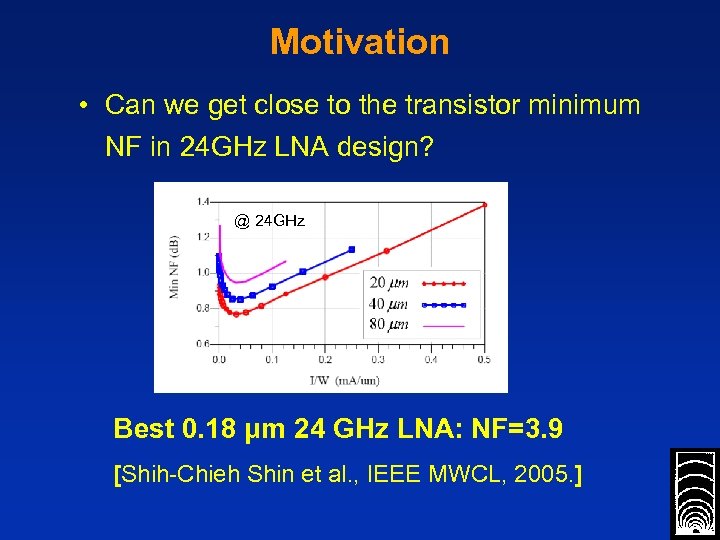 Motivation • Can we get close to the transistor minimum NF in 24 GHz LNA design? @ 24 GHz Best 0. 18 μm 24 GHz LNA: NF=3. 9 [Shih-Chieh Shin et al. , IEEE MWCL, 2005. ]
 LNA Design Methodology 1. Determine the optimal current density 2. Determine critical circuit element values 3. Choose the transistor width
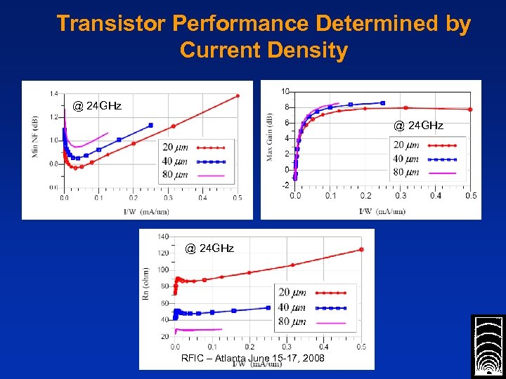 Transistor Performance Determined by Current Density @ 24 GHz RFIC – Atlanta June 15 -17, 2008
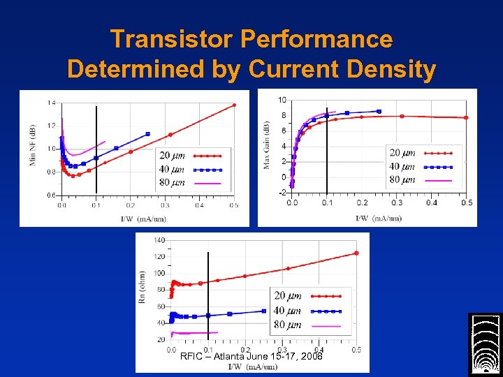 Transistor Performance Determined by Current Density RFIC – Atlanta June 15 -17, 2008
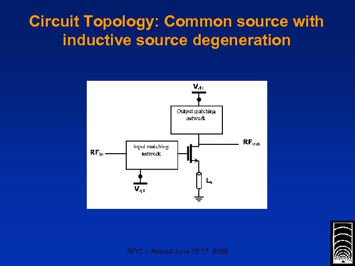 Circuit Topology: Common source with inductive source degeneration RFIC – Atlanta June 15 -17, 2008
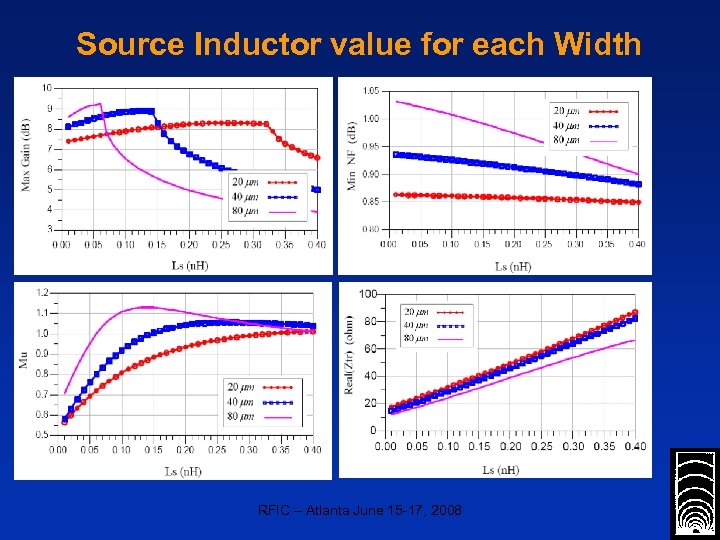 Source Inductor value for each Width RFIC – Atlanta June 15 -17, 2008
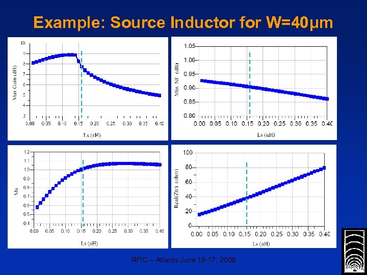 Example: Source Inductor for W=40μm RFIC – Atlanta June 15 -17, 2008
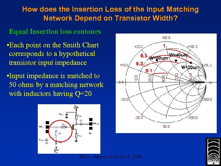 How does the Insertion Loss of the Input Matching Network Depend on Transistor Width? Equal Insertion loss contours • Each point on the Smith Chart corresponds to a hypothetical transistor input impedance • Input impedance is matched to 50 ohms by a matching network with inductors having Q=20 RFIC – Atlanta June 15 -17, 2008
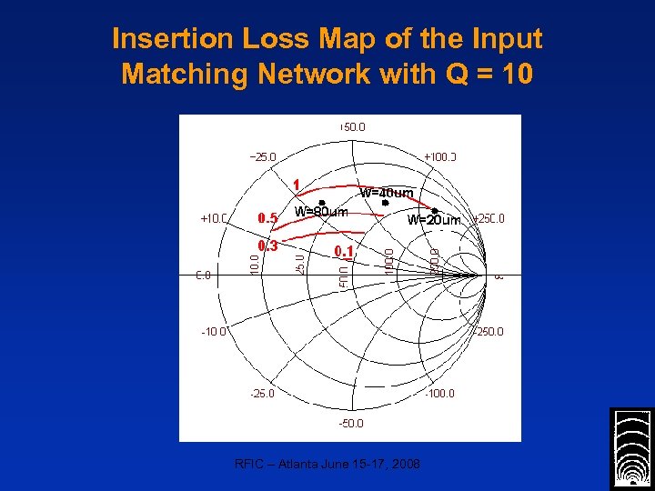 Insertion Loss Map of the Input Matching Network with Q = 10 RFIC – Atlanta June 15 -17, 2008
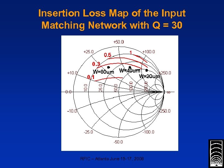 Insertion Loss Map of the Input Matching Network with Q = 30 RFIC – Atlanta June 15 -17, 2008
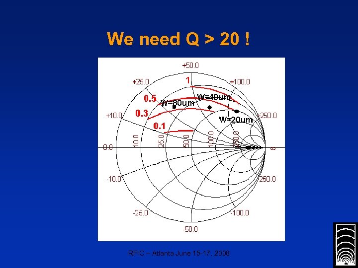 We need Q > 20 ! RFIC – Atlanta June 15 -17, 2008
![Choosing the Transistor Widths (assuming a two identical stage amplifier) W [um] Transistor Max Choosing the Transistor Widths (assuming a two identical stage amplifier) W [um] Transistor Max](https://present5.com/presentation/39aab218757f05a6bf5f0ac037266d4d/image-14.jpg) Choosing the Transistor Widths (assuming a two identical stage amplifier) W [um] Transistor Max Min NF [d. B] gs [d. B] NF total [d. B] Gain [d. B] 20 7. 2 0. 82 0. 3 1. 2 40 8 0. 9 0. 8 1. 3 80 8. 2 1 1. 44 1. 6 * g. S - normalized source gain factor RFIC – Atlanta June 15 -17, 2008
Choosing the Transistor Widths (assuming a two identical stage amplifier) W [um] Transistor Max Min NF [d. B] gs [d. B] NF total [d. B] Gain [d. B] 20 7. 2 0. 82 0. 3 1. 2 40 8 0. 9 0. 8 1. 3 80 8. 2 1 1. 44 1. 6 * g. S - normalized source gain factor RFIC – Atlanta June 15 -17, 2008
![Choosing the Transistor Widths (assuming a two identical stage amplifier) W [um] Max Gain Choosing the Transistor Widths (assuming a two identical stage amplifier) W [um] Max Gain](https://present5.com/presentation/39aab218757f05a6bf5f0ac037266d4d/image-15.jpg) Choosing the Transistor Widths (assuming a two identical stage amplifier) W [um] Max Gain Min NF [d. B] gs [d. B] NF total [d. B] 20 7. 2 0. 82 0. 3 1. 2 40 8 0. 9 0. 8 1. 3 80 8. 2 1 1. 44 1. 6 RFIC – Atlanta June 15 -17, 2008
Choosing the Transistor Widths (assuming a two identical stage amplifier) W [um] Max Gain Min NF [d. B] gs [d. B] NF total [d. B] 20 7. 2 0. 82 0. 3 1. 2 40 8 0. 9 0. 8 1. 3 80 8. 2 1 1. 44 1. 6 RFIC – Atlanta June 15 -17, 2008
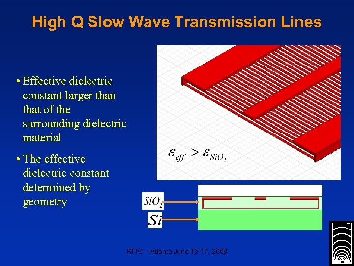 High Q Slow Wave Transmission Lines • Effective dielectric constant larger than that of the surrounding dielectric material • The effective dielectric constant determined by geometry RFIC – Atlanta June 15 -17, 2008
 Properties of Slow Wave TL • Isolation from the lossy silicon substrate • Shorter wavelength shorter matching networks • Lower loss per wave length higher Q of resonators • Smaller die area • Higher characteristic impedance • Complicated EM simulations • Complicated layout RFIC – Atlanta June 15 -17, 2008
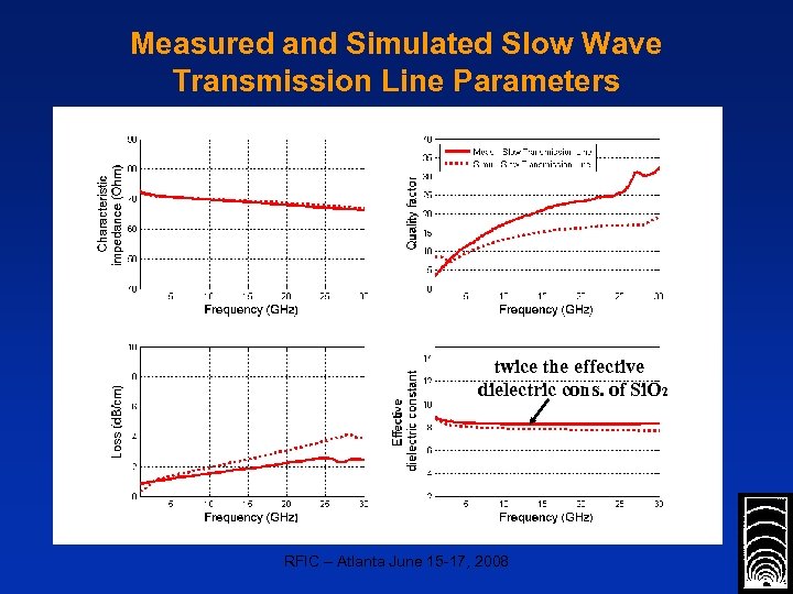 Measured and Simulated Slow Wave Transmission Line Parameters twice the effective dielectric cons. of Si. O 2 RFIC – Atlanta June 15 -17, 2008
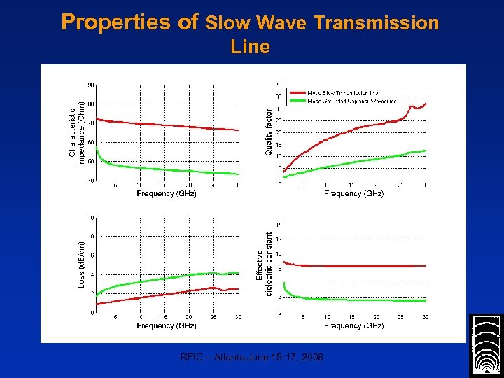 Properties of Slow Wave Transmission Line RFIC – Atlanta June 15 -17, 2008
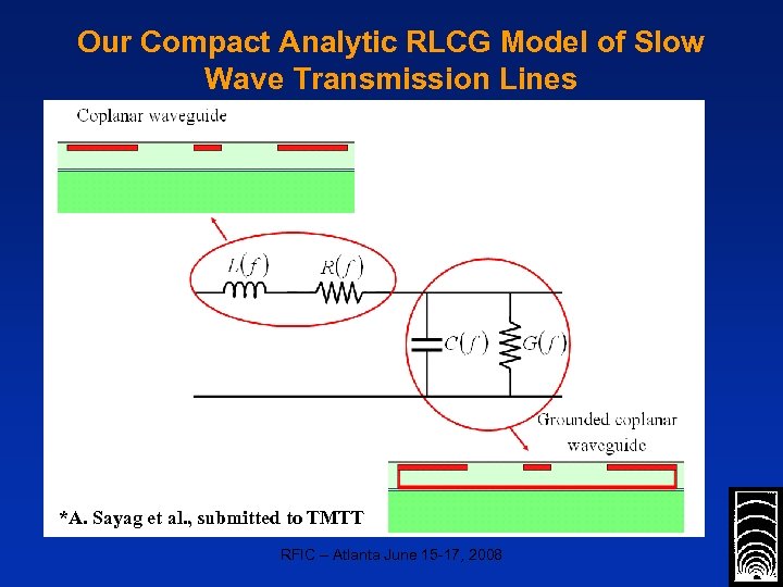 Our Compact Analytic RLCG Model of Slow Wave Transmission Lines *A. Sayag et al. , submitted to TMTT RFIC – Atlanta June 15 -17, 2008
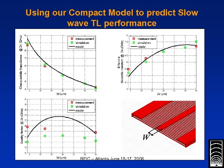 Using our Compact Model to predict Slow wave TL performance RFIC – Atlanta June 15 -17, 2008
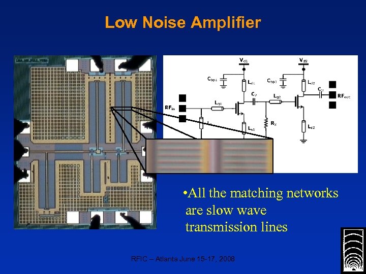 Low Noise Amplifier • All the matching networks are slow wave transmission lines RFIC – Atlanta June 15 -17, 2008
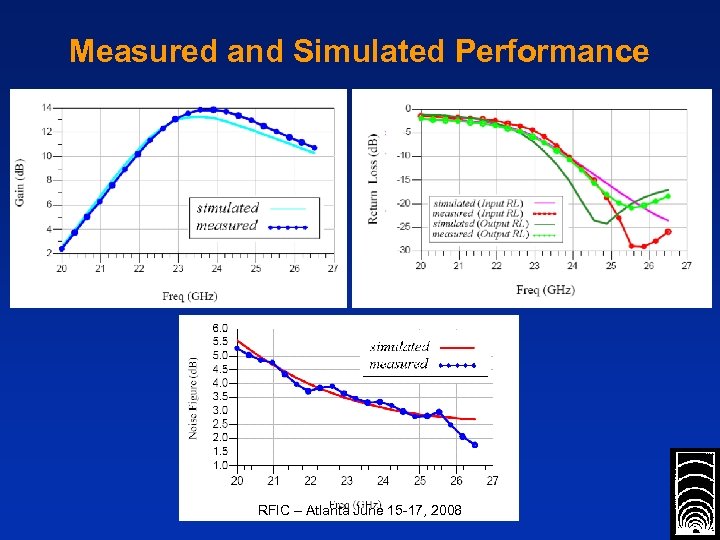 Measured and Simulated Performance RFIC – Atlanta June 15 -17, 2008
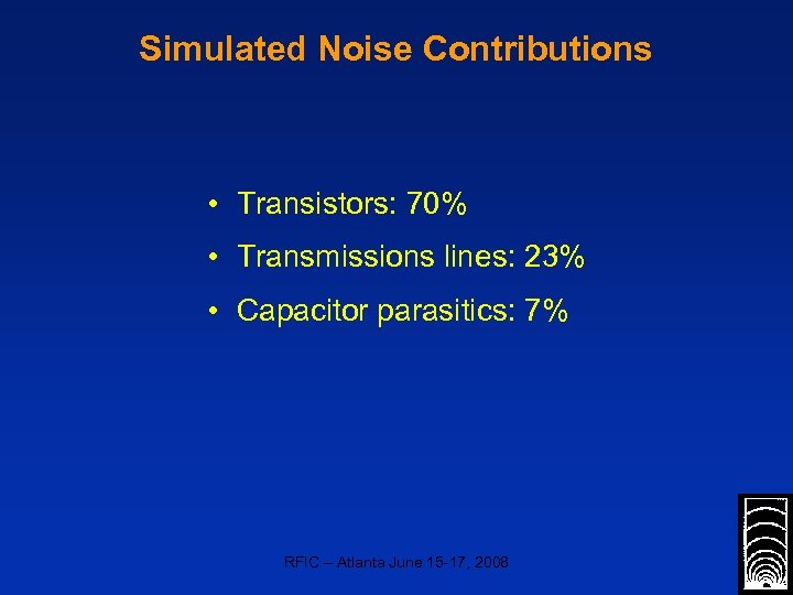 Simulated Noise Contributions • Transistors: 70% • Transmissions lines: 23% • Capacitor parasitics: 7% RFIC – Atlanta June 15 -17, 2008
![Comparison with State of the Art LNAs [1] [2] Shih-Chieh. Shin et al. , Comparison with State of the Art LNAs [1] [2] Shih-Chieh. Shin et al. ,](https://present5.com/presentation/39aab218757f05a6bf5f0ac037266d4d/image-25.jpg) Comparison with State of the Art LNAs [1] [2] Shih-Chieh. Shin et al. , IEEE Microwave and Wireless Component Letters, July, 2005. E. Adabi et al. , " RFIC Symposium, June 3 -5, 2007, Honolulu, Hawaii. RFIC – Atlanta June 15 -17, 2008
Comparison with State of the Art LNAs [1] [2] Shih-Chieh. Shin et al. , IEEE Microwave and Wireless Component Letters, July, 2005. E. Adabi et al. , " RFIC Symposium, June 3 -5, 2007, Honolulu, Hawaii. RFIC – Atlanta June 15 -17, 2008
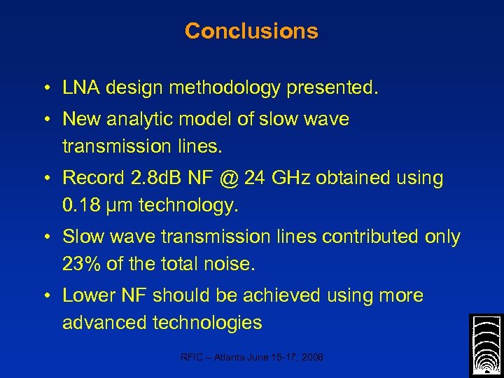 Conclusions • LNA design methodology presented. • New analytic model of slow wave transmission lines. • Record 2. 8 d. B NF @ 24 GHz obtained using 0. 18 μm technology. • Slow wave transmission lines contributed only 23% of the total noise. • Lower NF should be achieved using more advanced technologies RFIC – Atlanta June 15 -17, 2008
 Thank You! RFIC – Atlanta June 15 -17, 2008
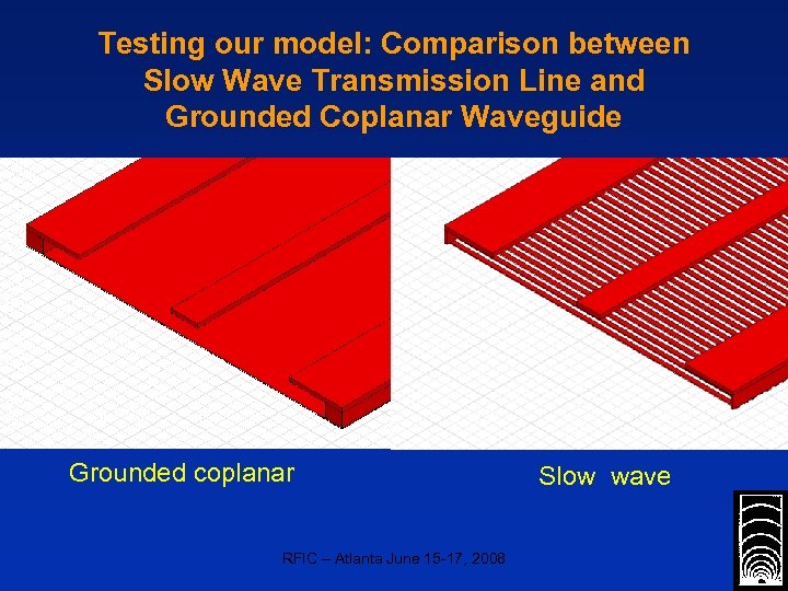 Testing our model: Comparison between Slow Wave Transmission Line and Grounded Coplanar Waveguide Grounded coplanar RFIC – Atlanta June 15 -17, 2008 Slow wave
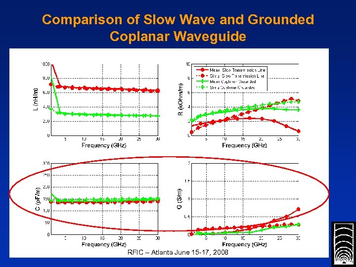 Comparison of Slow Wave and Grounded Coplanar Waveguide RFIC – Atlanta June 15 -17, 2008
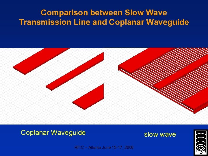 Comparison between Slow Wave Transmission Line and Coplanar Waveguide RFIC – Atlanta June 15 -17, 2008 slow wave
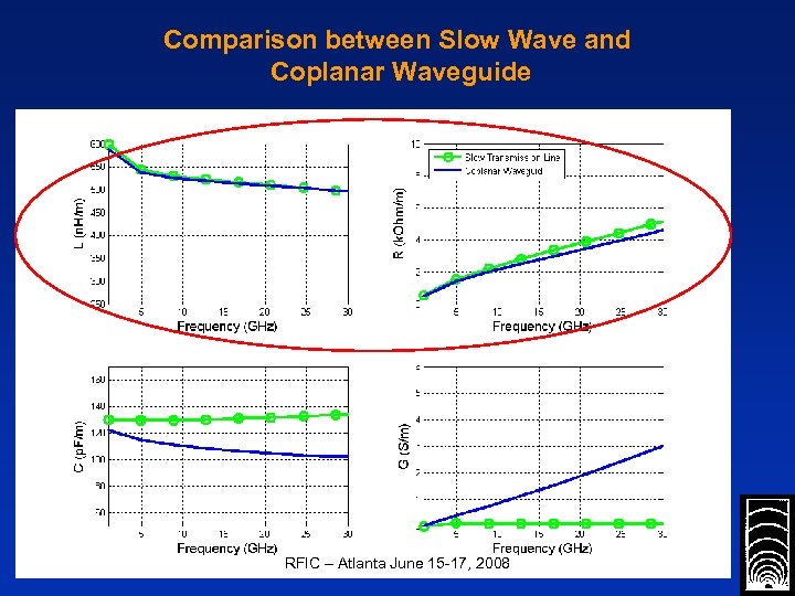 Comparison between Slow Wave and Coplanar Waveguide RFIC – Atlanta June 15 -17, 2008


