cb46495e6450acd7942f8124cc2987c0.ppt
- Количество слайдов: 17
 RPC Electronics Status • Overall system • TDC – Digitizing frequency issue • (determine the bin size of the TDC value) • Discriminator test result • Trigger module status • Fabrication
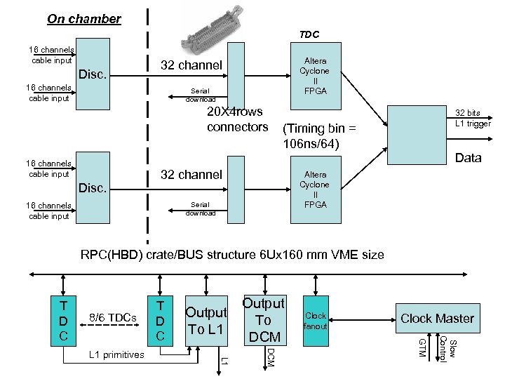 On chamber TDC 16 channels cable input Disc. Altera Cyclone II FPGA 32 channel 16 channels cable input Serial download 20 X 4 rows connectors 32 bits L 1 trigger (Timing bin = 106 ns/64) Data 16 channels cable input Disc. 32 channel Altera Cyclone II FPGA Serial download 16 channels cable input RPC(HBD) crate/BUS structure 6 Ux 160 mm VME size 8/6 TDCs Output To DCM Clock fanout Clock Master DCM Slow Control Output To L 1 L 1 primitives T D C GTM T D C
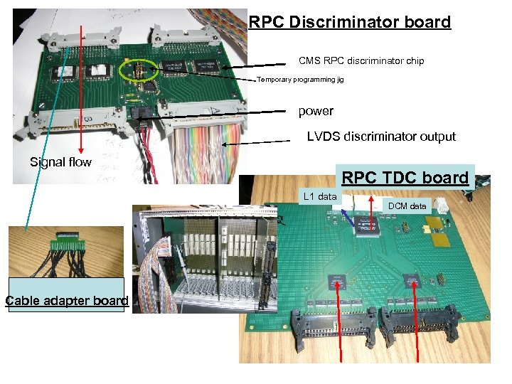 RPC Discriminator board CMS RPC discriminator chip Temporary programming jig power LVDS discriminator output Signal flow RPC TDC board L 1 data Cable adapter board DCM data
 TDC digitizing frequency issue • The FPGA uses 4 x beam clock to generating the digitizing frequency. This frequency drive a counter. Discriminator pulse stop the counter. => TDC value • Original idea is have use both edges of 320 MHz, 8*40 MHz, as TDC counter clock. One set per channel. 32 channel per chip – The circuit associate with positive and negative edges of the clock are routed as independent circuits. • The circuits associate with the positive and negative clock edges has slightly different delay than ½ clock cycle. • The two counters need to be aligned within 1. 65 ns to be useful. Otherwise one can not aligned the counters between positive and negative edge. • As an backup solution, we use 44* beam clock frequency as the clock for TDC counter, 2. 5 ns time bin with 9. 6 MHz RHIC clock. – This is still better than we claim in the CDR, i. e. 3. 3 ns. • In the mean time, we will still try to improve the 320 MHz compiling result.
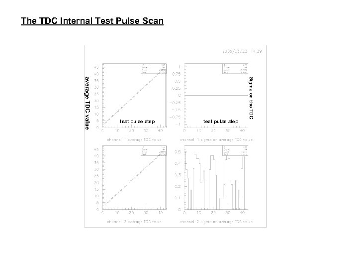 The TDC Internal Test Pulse Scan test pulse step Sigma on the TDC average TDC value test pulse step
 Discriminator test • One can inject test pulse into the CMS discriminator chip. – The test pulse couple into the input through ~1. 2 pf capacitor. The negative edge of the pulse need to come first. – This can be used to verify the cable or channel alive test. It is not mean to be used as calibration of the discriminator chips. • One can also inject pulse into the front end. – Threshold effect study. – Input pulse height scan. (to be done) • Test run for the Old and new chips. • Check for the 10 m cables drives
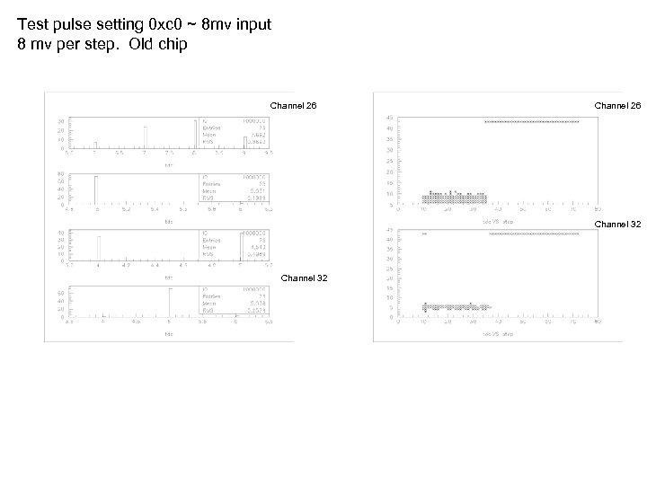 Test pulse setting 0 xc 0 ~ 8 mv input 8 mv per step. Old chip Channel 26 Channel 32
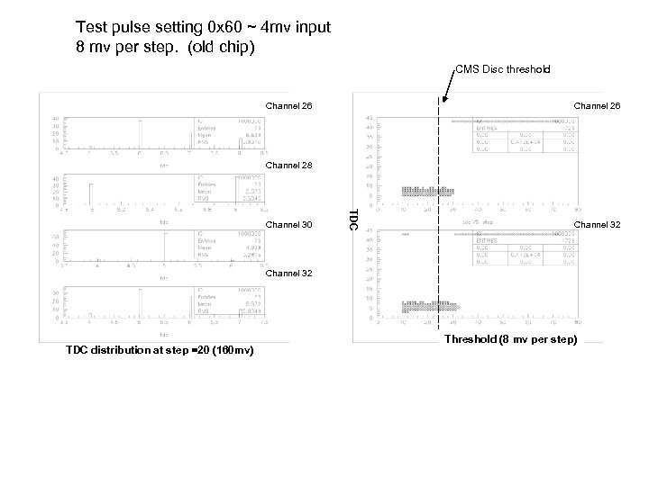 Test pulse setting 0 x 60 ~ 4 mv input 8 mv per step. (old chip) CMS Disc threshold Channel 26 Channel 28 TDC Channel 30 Channel 32 TDC distribution at step =20 (160 mv) Threshold (8 mv per step)
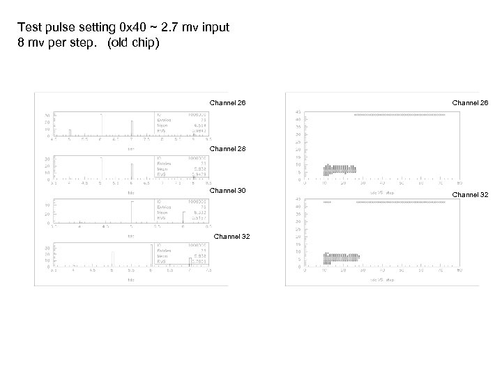 Test pulse setting 0 x 40 ~ 2. 7 mv input 8 mv per step. (old chip) Channel 26 Channel 28 Channel 30 Channel 32
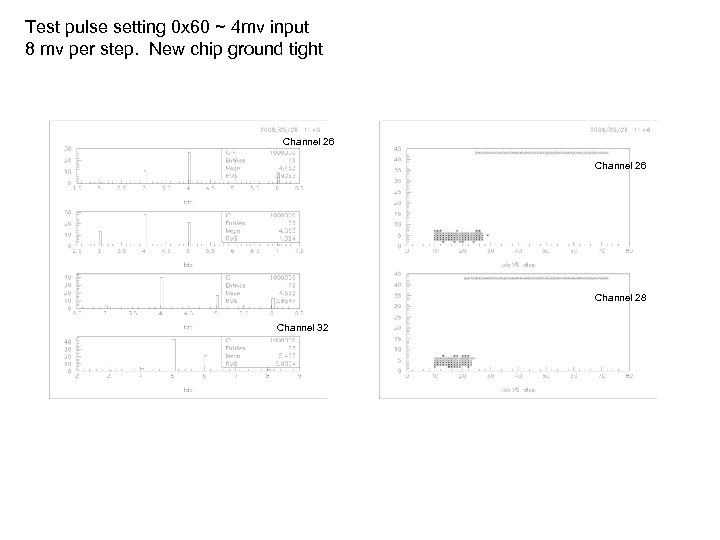 Test pulse setting 0 x 60 ~ 4 mv input 8 mv per step. New chip ground tight Channel 26 Channel 28 Channel 32
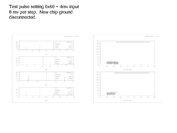 Test pulse setting 0 x 60 ~ 4 mv input 8 mv per step. New chip ground disconnected.
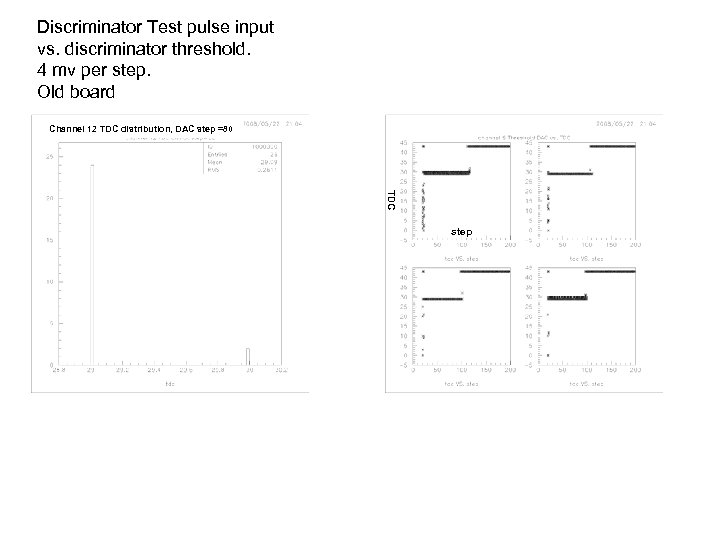 Discriminator Test pulse input vs. discriminator threshold. 4 mv per step. Old board Channel 12 TDC distribution, DAC step =80 TDC step
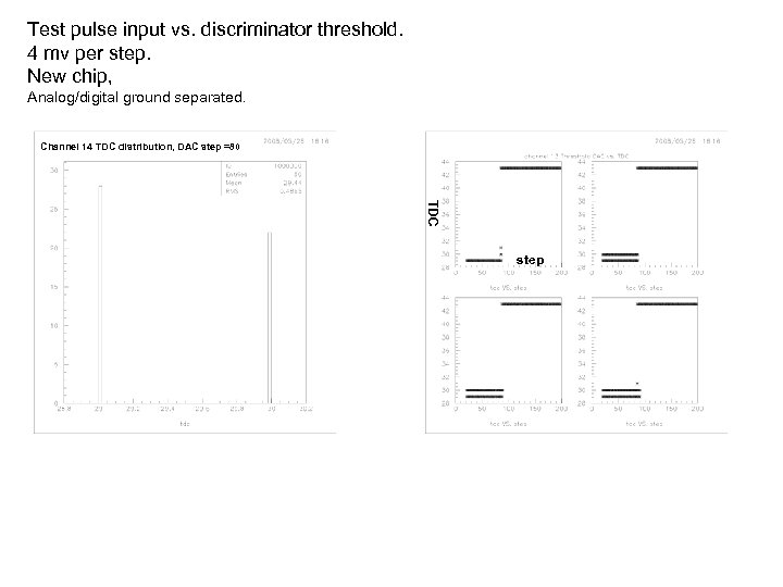 Test pulse input vs. discriminator threshold. 4 mv per step. New chip, Analog/digital ground separated. Channel 14 TDC distribution, DAC step =80 TDC step
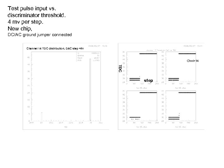 Test pulse input vs. discriminator threshold. 4 mv per step. New chip, DC/AC ground jumper connected Channel 14 TDC distribution, DAC step =80 Chnl=14 TDC step
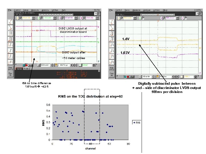 DISC LVDS output at discriminator board 1. 4 V DISC output after 1. 63 V ~10 meter cables 69 ns time difference 1. 61 ns/ft ~42 ft Digitally subtracted pulse between + and – side of discriminator LVDS output 500 mv per division
 Trigger Module • We have start to work on the trigger module FPGA code. – We will start with the design base on the possibility the strips will be connected at the detector, i. e. the FEM will output 64 trigger bits per beam clock. – There is no TDC module changes to accommodate this changes. • It will take us probably till late August/early September to finish all the coding and layout the board. • There is no budget to fabricate this board. – Fund are re-allocated to the purchase of the parts for the factory setup and coming run.
 Fabrication Status • We are starting to assemble the discriminator modules in house with the final cable connectors, >12 finished. • We have the clock master, clock fanout, TDC boards and parts. – Waiting for the purchase order for the assembly. • For backplane, we are waiting for the purchase order for the boards. • We need to work on the data taking software…


