5f2122bc56fdf71a8949b8b4dab72ea0.ppt
- Количество слайдов: 53
 RF Hardware System Design August 2009 – Version 1. 1 SHE
 Abstract • There are several aspects to consider when designing an RF system. This presentation discusses – – – Regulations How to select correct IC for the application HW design issues PCB layout issues HW testing • There also links to resources provided by TI to make it easier for customers to finalize their products.
 Outline • Planning and Evaluation Phase – Regulations – Selecting correct IC for the application • Development Phase – – – Decoupling capacitors Crystal Balun Range extension Powering LPRF products PCB layout • Test Phase – Test equipment – HW testing
 Planning and Evaluation Phase - Regulations - Selecting correct chip for the application
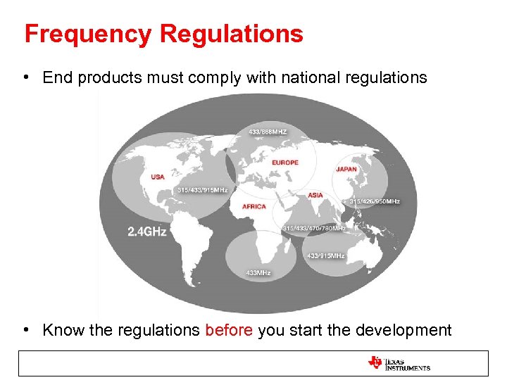 Frequency Regulations • End products must comply with national regulations • Know the regulations before you start the development
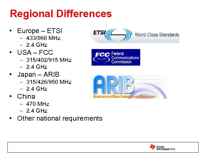 Regional Differences • Europe – ETSI – 433/868 MHz – 2. 4 GHz • USA – FCC – 315/402/915 MHz – 2. 4 GHz • Japan – ARIB – 315/426/950 MHz – 2. 4 GHz • China – 470 MHz – 2. 4 GHz • Other national requirements
 Regulatory Requirements • Before starting any development you need to look into and understand the regulatory requirements – – – – – Frequency bands Output power Spurious emission Adjacent channel power Occupied bandwidth Sensitivity Selectivity and blocking Duty cycle Listen Before Talk Frequency hopping
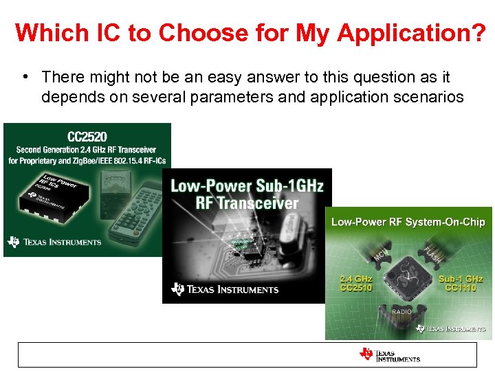 Which IC to Choose for My Application? • There might not be an easy answer to this question as it depends on several parameters and application scenarios
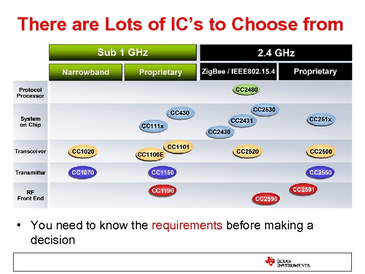 There are Lots of IC’s to Choose from CC 1190 • You need to know the requirements before making a decision
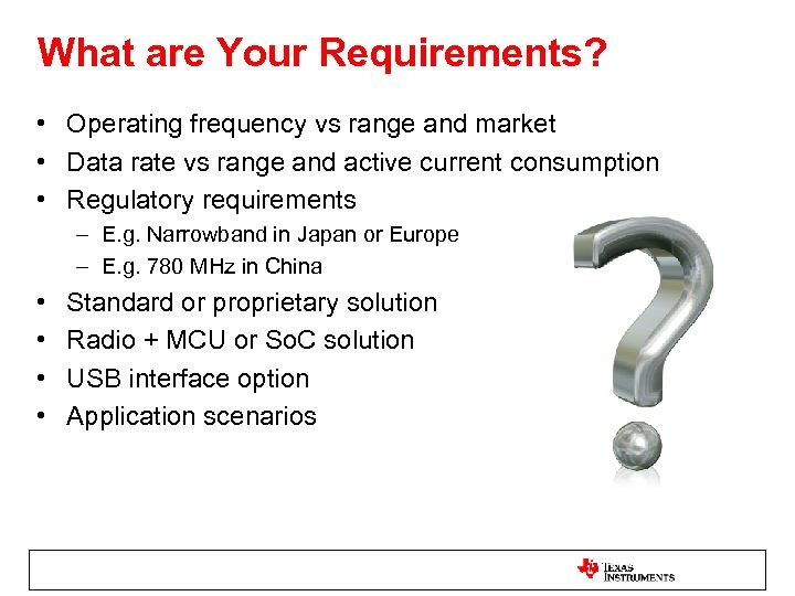 What are Your Requirements? • Operating frequency vs range and market • Data rate vs range and active current consumption • Regulatory requirements – E. g. Narrowband in Japan or Europe – E. g. 780 MHz in China • • Standard or proprietary solution Radio + MCU or So. C solution USB interface option Application scenarios
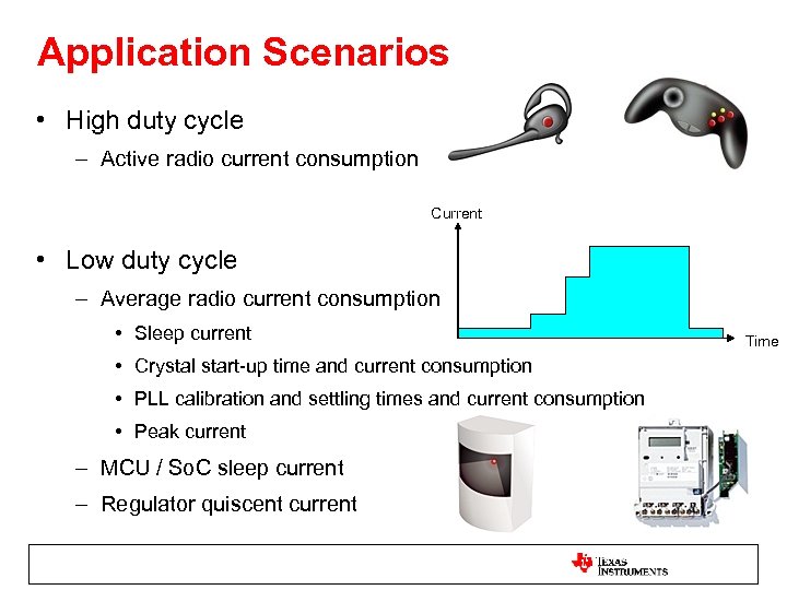 Application Scenarios • High duty cycle – Active radio current consumption Current • Low duty cycle – Average radio current consumption • Sleep current • Crystal start-up time and current consumption • PLL calibration and settling times and current consumption • Peak current – MCU / So. C sleep current – Regulator quiscent current Time
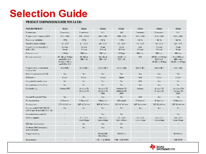 Selection Guide
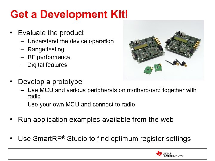 Get a Development Kit! • Evaluate the product – – Understand the device operation Range testing RF performance Digital features • Develop a prototype – Use MCU and various peripherals on motherboard together with radio – Use your own MCU and connect to radio • Run application examples available from the web • Use Smart. RF® Studio to find optimum register settings
 Do not Hesitate to Ask for Help • Ask for help at an early stage – – Do not wait until you are into the development phase Reduce time to market Minimize development risk Sometimes an RF specialists is required • Contact your local FAE • Customer Support http: //www. ti. com/support Email, Product Information Centers: Americas, EMEA, Japan, Asia • TI LP RF forum / E 2 E community http: //www. ti. com/lprf-forum
 Additional Resources • FAQs: https: //community. ti. com/forums/51. aspx • DN: https: //community. ti. com/search/Search. Results. aspx? tag=DN&or. Tags=0 • AN: https: //community. ti. com/search/Search. Results. aspx? tag=AN&or. Tags=0 • New Low-Power RF Selection Guide • Low-Power RF Newsletter – – – – New products Updated selection tables More tools, software, technical documents www. ti. com/lprfguide Software and hardware updates Developers’ news Latest application and design notes www. ti. com/lprfnewsletter
 Development Phase - Decoupling capacitors - Crystal - Balun - Range extension - Powering LPRF products - PCB layout
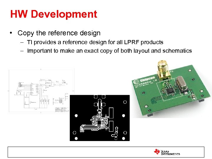 HW Development • Copy the reference design – TI provides a reference design for all LPRF products – Important to make an exact copy of both layout and schematics
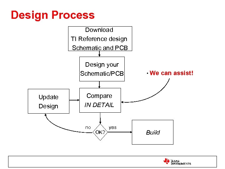 Design Process Download TI Reference design Schematic and PCB Design your Schematic/PCB Update Design • We Compare IN DETAIL no OK? yes Build can assist!
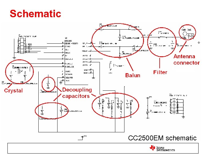 Schematic CC 2500 EM schematic
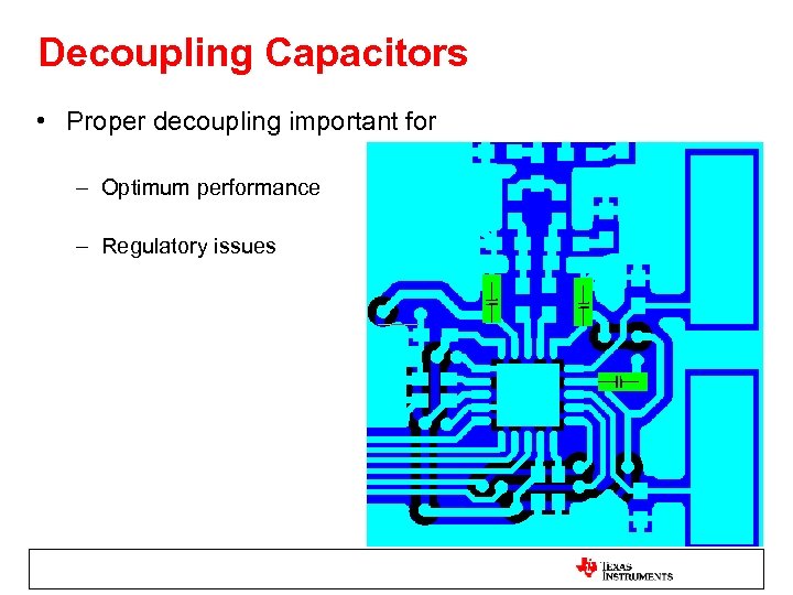 Decoupling Capacitors • Proper decoupling important for – Optimum performance – Regulatory issues
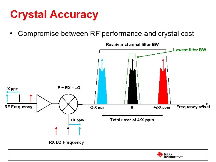 Crystal Accuracy • Compromise between RF performance and crystal cost Receiver channel filter BW Lowest filter BW -X ppm IF = RX - LO RF Frequency -2·X ppm +X ppm RX LO Frequency 0 +2·X ppm Total error of 4·X ppm Frequency offset
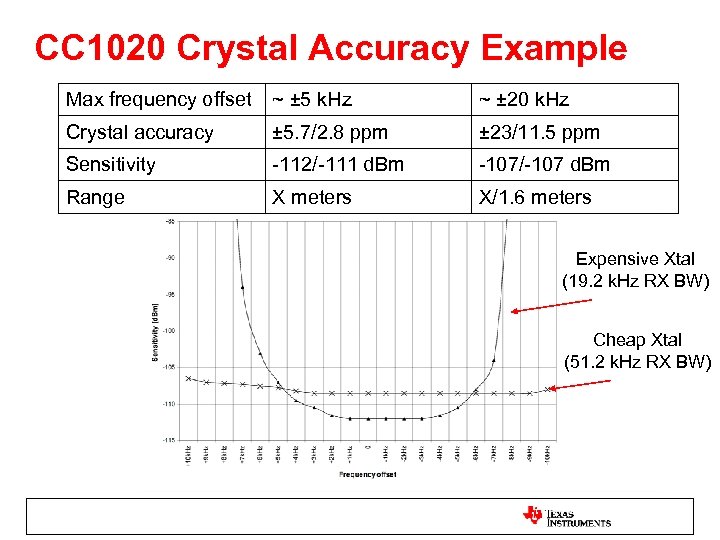 CC 1020 Crystal Accuracy Example Max frequency offset ~ ± 5 k. Hz ~ ± 20 k. Hz Crystal accuracy ± 5. 7/2. 8 ppm ± 23/11. 5 ppm Sensitivity -112/-111 d. Bm -107/-107 d. Bm Range X meters X/1. 6 meters Expensive Xtal (19. 2 k. Hz RX BW) Cheap Xtal (51. 2 k. Hz RX BW)
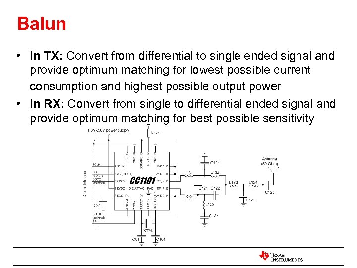 Balun • In TX: Convert from differential to single ended signal and provide optimum matching for lowest possible current consumption and highest possible output power • In RX: Convert from single to differential ended signal and provide optimum matching for best possible sensitivity
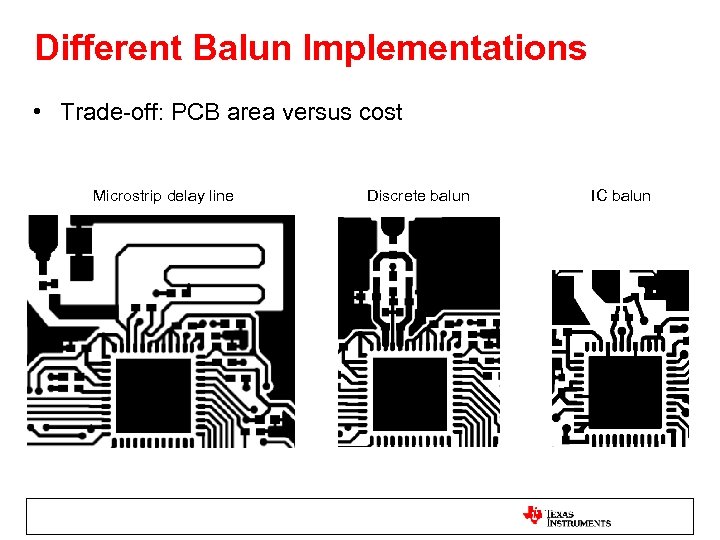 Different Balun Implementations • Trade-off: PCB area versus cost Microstrip delay line Discrete balun IC balun
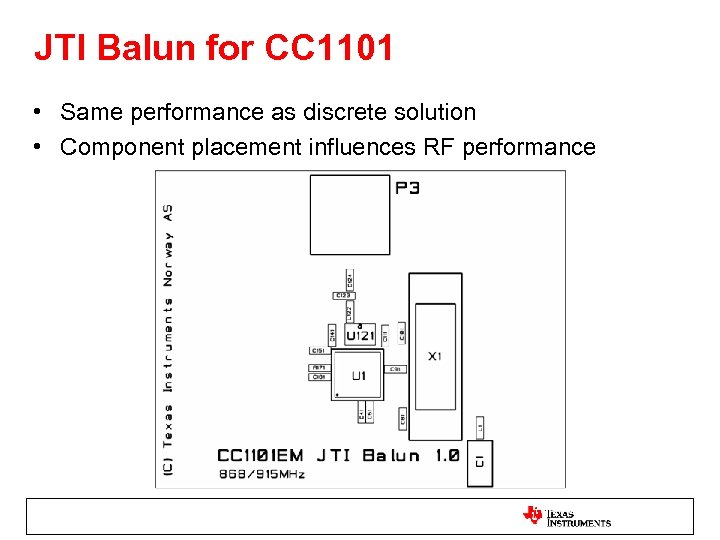 JTI Balun for CC 1101 • Same performance as discrete solution • Component placement influences RF performance
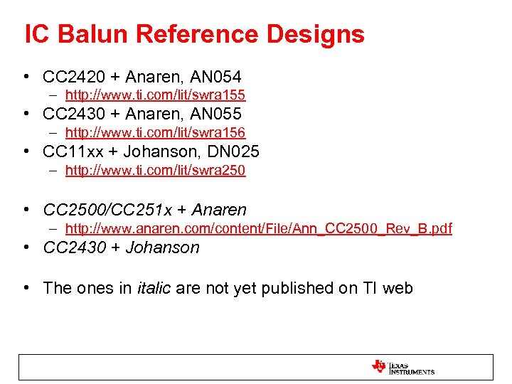 IC Balun Reference Designs • CC 2420 + Anaren, AN 054 – http: //www. ti. com/lit/swra 155 • CC 2430 + Anaren, AN 055 – http: //www. ti. com/lit/swra 156 • CC 11 xx + Johanson, DN 025 – http: //www. ti. com/lit/swra 250 • CC 2500/CC 251 x + Anaren – http: //www. anaren. com/content/File/Ann_CC 2500_Rev_B. pdf • CC 2430 + Johanson • The ones in italic are not yet published on TI web
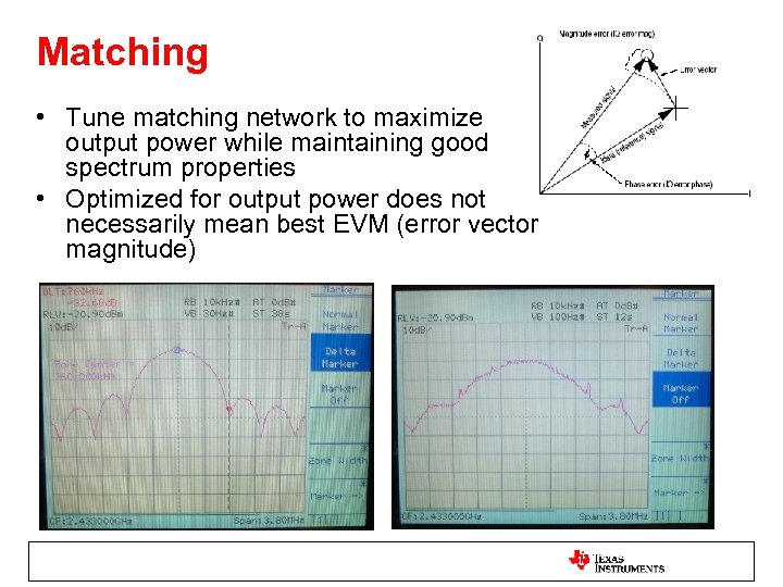 Matching • Tune matching network to maximize output power while maintaining good spectrum properties • Optimized for output power does not necessarily mean best EVM (error vector magnitude)
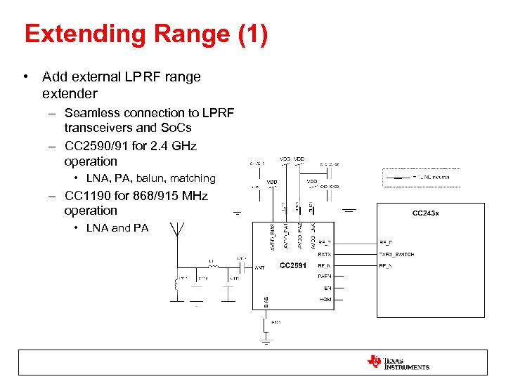 Extending Range (1) • Add external LPRF range extender – Seamless connection to LPRF transceivers and So. Cs – CC 2590/91 for 2. 4 GHz operation • LNA, PA, balun, matching – CC 1190 for 868/915 MHz operation • LNA and PA
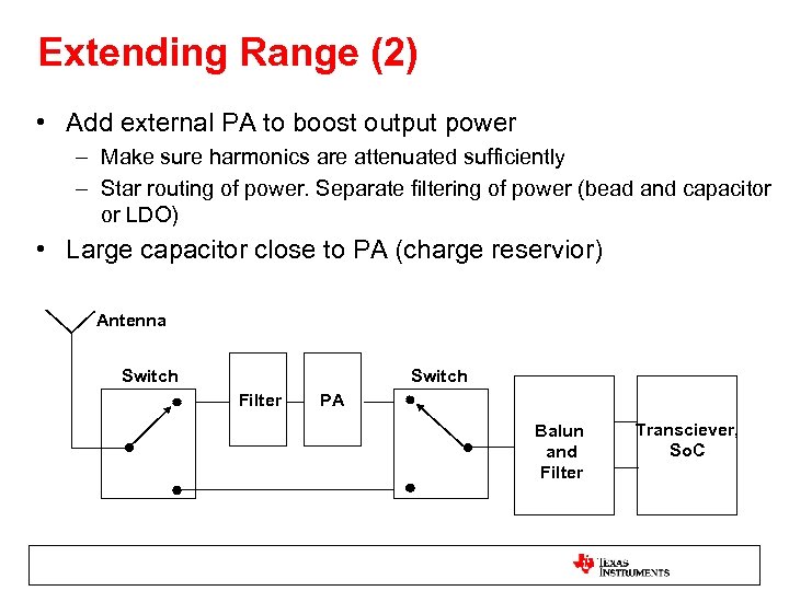 Extending Range (2) • Add external PA to boost output power – Make sure harmonics are attenuated sufficiently – Star routing of power. Separate filtering of power (bead and capacitor or LDO) • Large capacitor close to PA (charge reservior) Antenna Switch Filter PA Balun and Filter Transciever, So. C
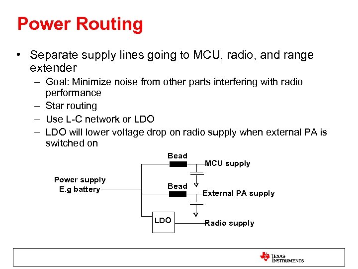 Power Routing • Separate supply lines going to MCU, radio, and range extender – Goal: Minimize noise from other parts interfering with radio performance – Star routing – Use L-C network or LDO – LDO will lower voltage drop on radio supply when external PA is switched on Bead Power supply E. g battery Bead LDO MCU supply External PA supply Radio supply
 Powering LPRF Products • Batteries • Linear Voltage Regulators – LDO’s are special type which converts even with a low voltage difference • Switch Mode DC/DC Converters – Buck – Boost – Buck-boost
 Linear Voltage Regulators • Efficiency: η ~ Vout/Vin – e. g 3. 6 V supply and 1. 8 V operating voltage ~ 50% • Iin = Iout – Power is lost as heat (Pdiss = (Vout – Vout)∙Iout) • Advantage – – – Good Power Supply Ripple Rejection (PSRR) Few external components Inexpensive Small in size ”Quite” (no switching)
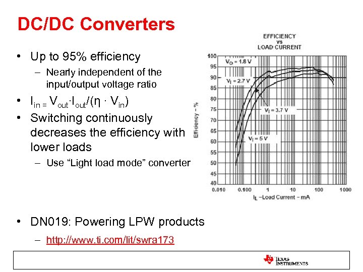 DC/DC Converters • Up to 95% efficiency – Nearly independent of the input/output voltage ratio • Iin = Vout∙Iout/(η ∙ Vin) • Switching continuously decreases the efficiency with lower loads – Use “Light load mode” converter • DN 019: Powering LPW products – http: //www. ti. com/lit/swra 173
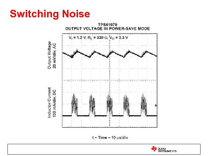 Switching Noise
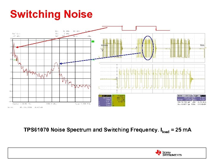 Switching Noise TPS 61070 Noise Spectrum and Switching Frequency. Iload = 25 m. A
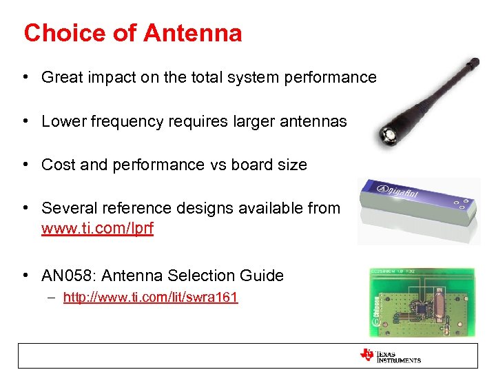 Choice of Antenna • Great impact on the total system performance • Lower frequency requires larger antennas • Cost and performance vs board size • Several reference designs available from www. ti. com/lprf • AN 058: Antenna Selection Guide – http: //www. ti. com/lit/swra 161
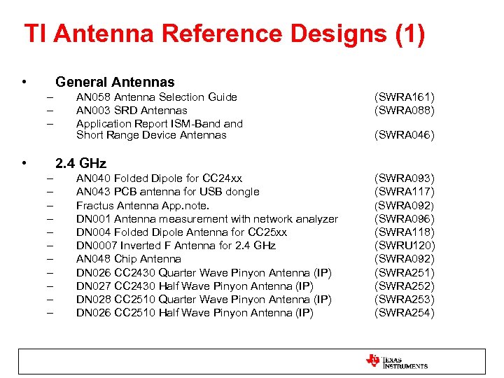 TI Antenna Reference Designs (1) • General Antennas – – – • AN 058 Antenna Selection Guide AN 003 SRD Antennas Application Report ISM-Band Short Range Device Antennas (SWRA 161) (SWRA 088) (SWRA 046) 2. 4 GHz – – – AN 040 Folded Dipole for CC 24 xx AN 043 PCB antenna for USB dongle Fractus Antenna App. note. DN 001 Antenna measurement with network analyzer DN 004 Folded Dipole Antenna for CC 25 xx DN 0007 Inverted F Antenna for 2. 4 GHz AN 048 Chip Antenna DN 026 CC 2430 Quarter Wave Pinyon Antenna (IP) DN 027 CC 2430 Half Wave Pinyon Antenna (IP) DN 028 CC 2510 Quarter Wave Pinyon Antenna (IP) DN 026 CC 2510 Half Wave Pinyon Antenna (IP) (SWRA 093) (SWRA 117) (SWRA 092) (SWRA 096) (SWRA 118) (SWRU 120) (SWRA 092) (SWRA 251) (SWRA 252) (SWRA 253) (SWRA 254)
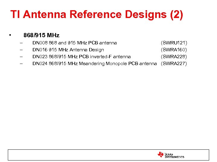 TI Antenna Reference Designs (2) • 868/915 MHz – – DN 008 868 and 915 MHz PCB antenna DN 016 915 MHz Antenna Design DN 023 868/915 MHz PCB inverted-F antenna DN 024 868/915 MHz Meandering Monopole PCB antenna (SWRU 121) (SWRA 160) (SWRA 228) (SWRA 227)
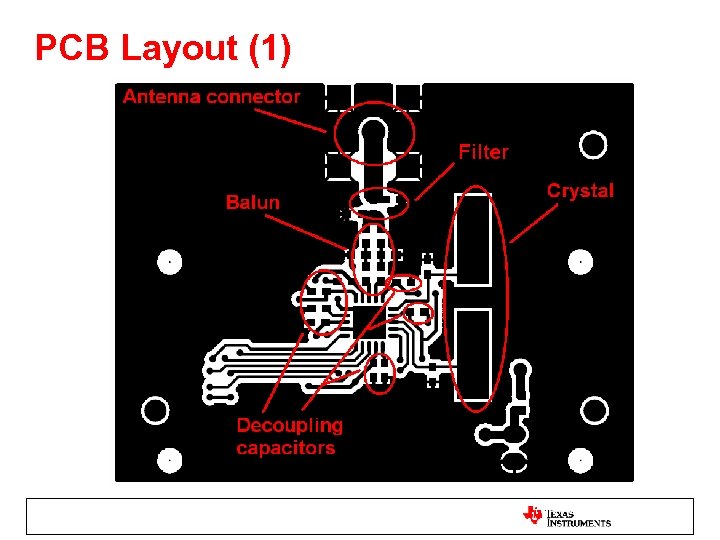 PCB Layout (1)
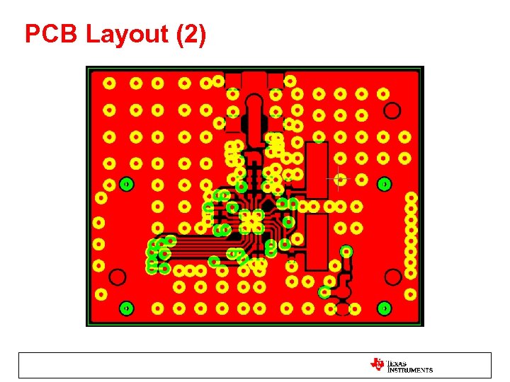 PCB Layout (2)
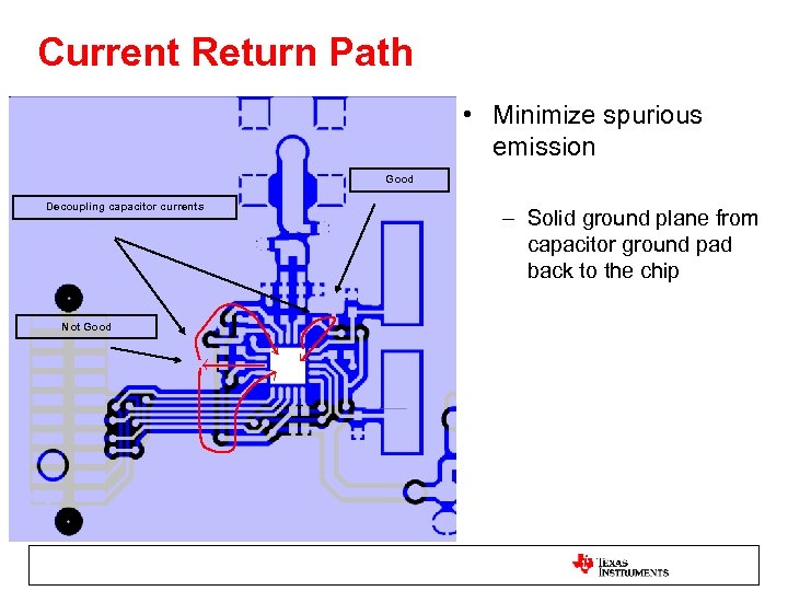 Current Return Path • Minimize spurious emission Good Decoupling capacitor currents Not Good – Solid ground plane from capacitor ground pad back to the chip
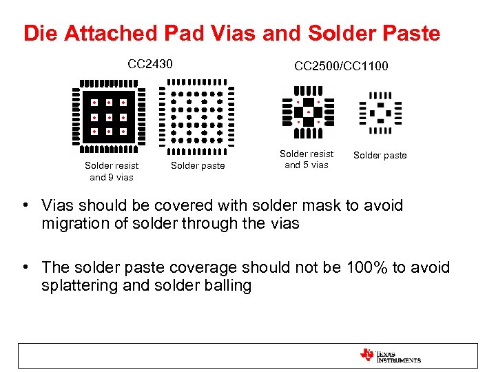 Die Attached Pad Vias and Solder Paste CC 2430 Solder resist and 9 vias Solder paste CC 2500/CC 1100 Solder resist and 5 vias Solder paste • Vias should be covered with solder mask to avoid migration of solder through the vias • The solder paste coverage should not be 100% to avoid splattering and solder balling
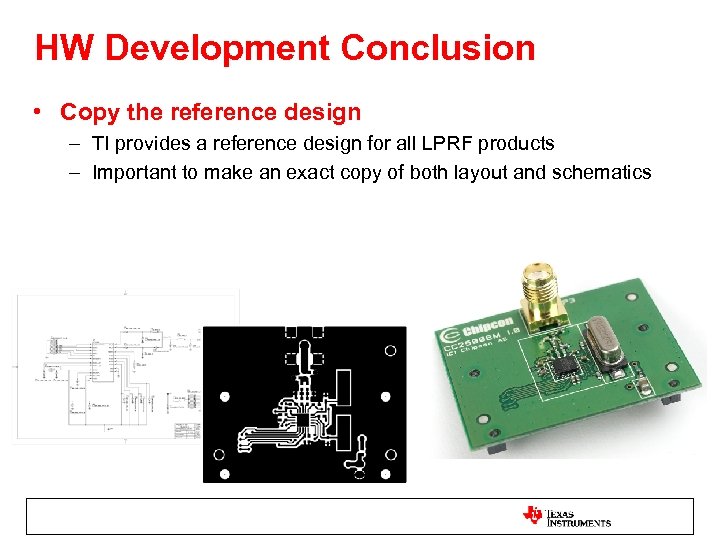 HW Development Conclusion • Copy the reference design – TI provides a reference design for all LPRF products – Important to make an exact copy of both layout and schematics
 Test Phase - Test equipment - HW testing
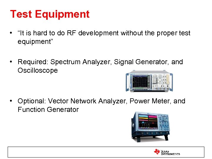 Test Equipment • “It is hard to do RF development without the proper test equipment” • Required: Spectrum Analyzer, Signal Generator, and Oscilloscope • Optional: Vector Network Analyzer, Power Meter, and Function Generator
 How and What to Test? • Testing shall be divided up in separate parts, independent of each other • Hardware, software, and antenna shall be tested separately
 Narrow Down the Problem • Check if the problem is SW or HW related – Test the SW with well-known working HW, evaluation modules – Test the HW with well-known working SW, Smart. RF® Studio • If it is hardware related: – Compare the design with our reference design – Check mounting of the chip and other components – Mount the radio on our EVM to check if the chip is damaged • If it is software related: – Compare the code with our software examples and libraries – Test the functionality of each “module” to isolate the problem – Compare register settings with values in Smart. RF® Studio
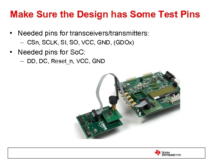 Make Sure the Design has Some Test Pins • Needed pins for transceivers/transmitters: – CSn, SCLK, SI, SO, VCC, GND, (GDOx) • Needed pins for So. C: – DD, DC, Reset_n, VCC, GND
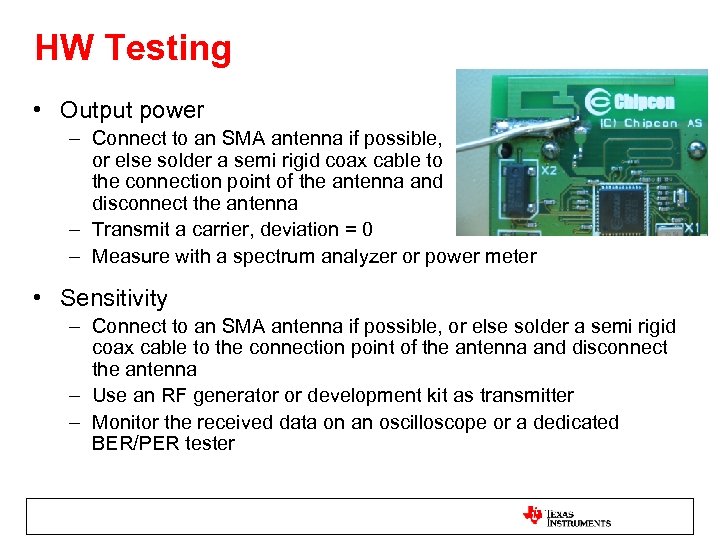 HW Testing • Output power – Connect to an SMA antenna if possible, or else solder a semi rigid coax cable to the connection point of the antenna and disconnect the antenna – Transmit a carrier, deviation = 0 – Measure with a spectrum analyzer or power meter • Sensitivity – Connect to an SMA antenna if possible, or else solder a semi rigid coax cable to the connection point of the antenna and disconnect the antenna – Use an RF generator or development kit as transmitter – Monitor the received data on an oscilloscope or a dedicated BER/PER tester
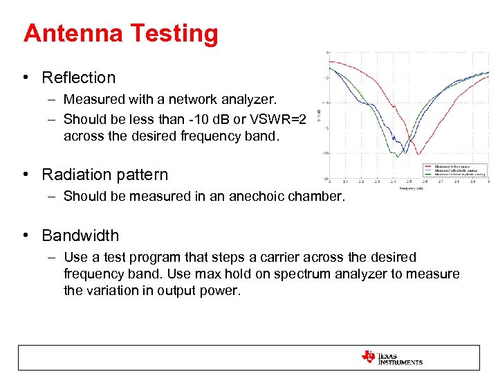 Antenna Testing • Reflection – Measured with a network analyzer. – Should be less than -10 d. B or VSWR=2 across the desired frequency band. • Radiation pattern – Should be measured in an anechoic chamber. • Bandwidth – Use a test program that steps a carrier across the desired frequency band. Use max hold on spectrum analyzer to measure the variation in output power.
 Radiated Tests are Required • When testing for regulatory compliance radiated tests are required • There might be a difference in radiated and conducted performance – Spurious emission might be attenuated by the finite antenna bandwidth – Spurious emission might be radiated from the PCB itself or components on the PCB resulting in increased spurious emission in radiated measurements
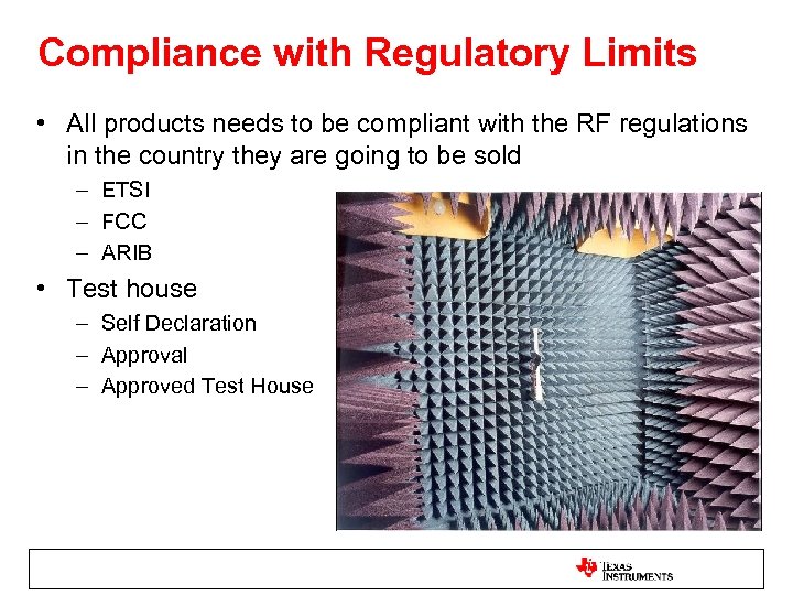 Compliance with Regulatory Limits • All products needs to be compliant with the RF regulations in the country they are going to be sold – ETSI – FCC – ARIB • Test house – Self Declaration – Approval – Approved Test House
 Questions?


