807cb229438fb8852e16287117dffe21.ppt
- Количество слайдов: 13
 Research Activities at UW for TTC Günter Müller Physics Department, University of Wuppertal, Germany gmueller@uni-wuppertal. de • • • Motivation DC Field Emission Scanning Microscopy on Nb Samples High Resolution SEM/EDX for Field Emitter Identification Surface Roughness Measurements with OP/AFM on Nb Photo-induced FE for High Brightness Electron Sources Outlook and acknowledgments G. Müller, 01. 03. 2011 Milano Meeting
 Motivation Further progress of superconducting electron linacs towards fundamental limits requires advanced material science which can be provided by universities. Enhanced field emission (EFE) from imperfect surfaces is a major limitation for achievable accelerating gradients in Nb cavities (Ep = 50 -120 MV/m !). In order to avoid EFE reliably, its physical origin must be understood, e. g. by means of localisation and idenfication of emitters on samples. Local quenches and enhanced losses The final surface quality resulting for in high magnetic surface fie. Id regions poly/single crystalline EP & BCP Nb (Hp → Hcrf) should depend on the local should be measured systematically and average surface roughness of Nb. and correlated to EFE & Quenches. Actual photocathodes used in rf guns (e. g. FLASH) provide short bunches but also high transverse emittance and have a short lifetime even under UHV. G. Müller, 01. 03. 2011 Photo-induced field emission (PFE) from flat metallic or semiconducting cathodes could lead to robust high brightness rf guns (e. g. XFEL). Milano Meeting
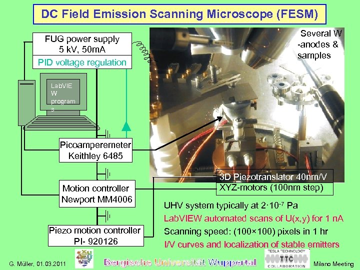 DC Field Emission Scanning Microscope (FESM) FUG power supply 5 k. V, 50 m. A PID voltage regulation Several W -anodes & samples Lab. VIE W program s Picoamperemeter Keithley 6485 Motion controller Newport MM 4006 Piezo motion controller PI- 920126 G. Müller, 01. 03. 2011 3 D Piezotranslator 40 nm/V XYZ-motors (100 nm step) UHV system typically at 2· 10 -7 Pa Lab. VIEW automated scans of U(x, y) for 1 n. A Scanning speed: (100× 100) pixels in 1 hr I/V curves and localization of stable emitters Milano Meeting
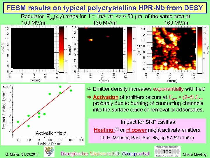 FESM results on typical polycrystalline HPR-Nb from DESY Regulated Eon(x, y) maps for I = 1 n. A at ∆z ≈ 50 µm of the same area at 100 MV/m 130 MV/m 160 MV/m ð Emitter density increases exponentially with field ð Activation of emitters occurs at Eact = (2 -4) Eon probably due to burning of conducting channels into the surface oxide or removal of adsorbates. Impact for SRF cavities: Activation field G. Müller, 01. 03. 2011 Heating [1] or rf power might activate emitters [1] E. Mahner, Part. Acc. 46, pp. 67 -82 (1994) Milano Meeting
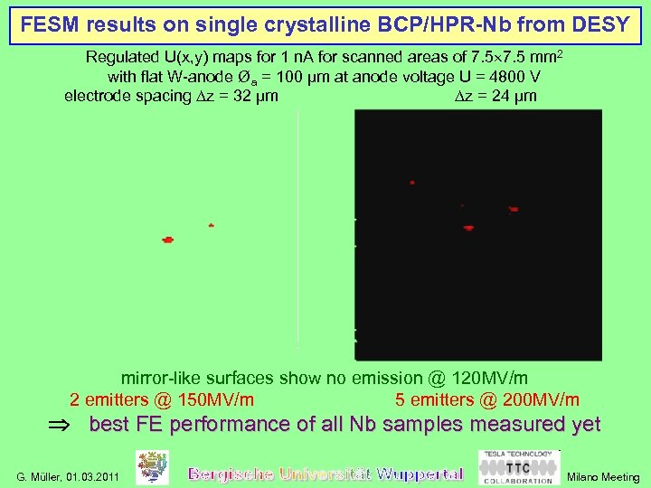 FESM results on single crystalline BCP/HPR-Nb from DESY Regulated U(x, y) maps for 1 n. A for scanned areas of 7. 5 mm 2 with flat W-anode Øa = 100 µm at anode voltage U = 4800 V electrode spacing Dz = 32 µm Dz = 24 µm mirror-like surfaces show no emission @ 120 MV/m 2 emitters @ 150 MV/m 5 emitters @ 200 MV/m best FE performance of all Nb samples measured yet G. Müller, 01. 03. 2011 Milano Meeting
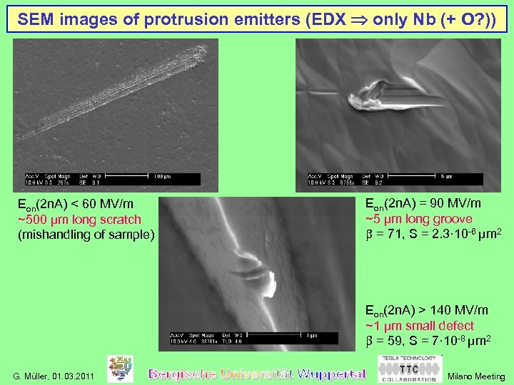 SEM images of protrusion emitters (EDX only Nb (+ O? )) Eon(2 n. A) < 60 MV/m ~500 µm long scratch (mishandling of sample) Eon(2 n. A) = 90 MV/m ~5 µm long groove = 71, S = 2. 3· 10 -6 µm 2 Eon(2 n. A) > 140 MV/m ~1 µm small defect = 59, S = 7· 10 -8 µm 2 G. Müller, 01. 03. 2011 Milano Meeting
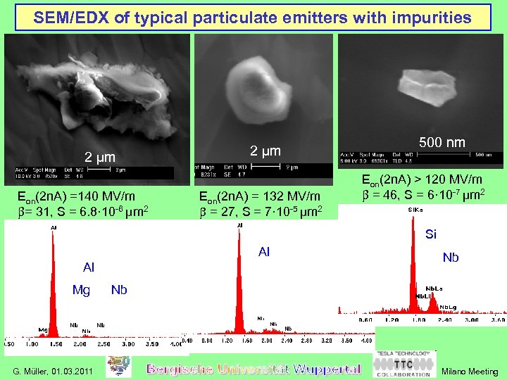 SEM/EDX of typical particulate emitters with impurities 2 µm Eon(2 n. A) =140 MV/m = 31, S = 6. 8· 10 -6 µm 2 2 µm Eon(2 n. A) = 132 MV/m = 27, S = 7· 10 -5 µm 2 500 nm Eon(2 n. A) > 120 MV/m = 46, S = 6· 10 -7 µm 2 Si Al Al Mg G. Müller, 01. 03. 2011 Nb Nb Milano Meeting
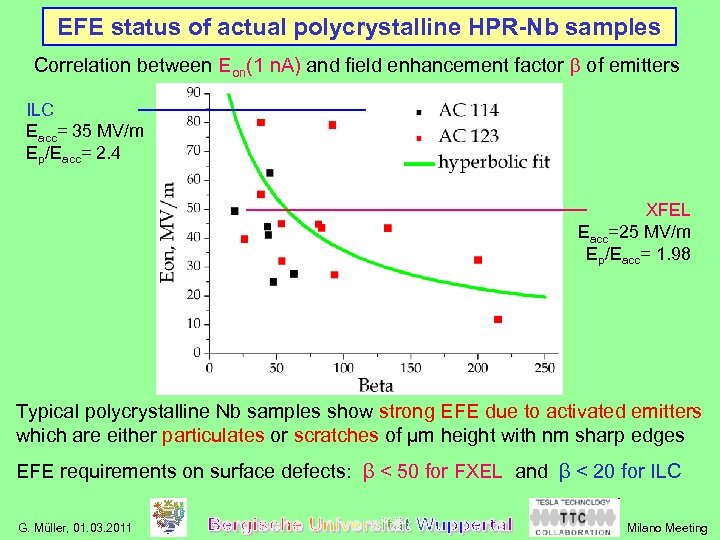 EFE status of actual polycrystalline HPR-Nb samples Correlation between Eon(1 n. A) and field enhancement factor of emitters ILC Eacc= 35 MV/m Ep/Eacc= 2. 4 XFEL Eacc=25 MV/m Ep/Eacc= 1. 98 Typical polycrystalline Nb samples show strong EFE due to activated emitters which are either particulates or scratches of µm height with nm sharp edges EFE requirements on surface defects: β < 50 for FXEL and β < 20 for ILC G. Müller, 01. 03. 2011 Milano Meeting
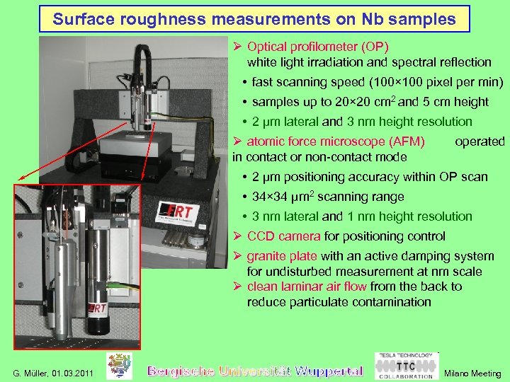 Surface roughness measurements on Nb samples Ø Optical profilometer (OP) white light irradiation and spectral reflection • fast scanning speed (100× 100 pixel per min) • samples up to 20× 20 cm 2 and 5 cm height • 2 µm lateral and 3 nm height resolution Ø atomic force microscope (AFM) in contact or non-contact mode operated • 2 µm positioning accuracy within OP scan • 34× 34 µm 2 scanning range • 3 nm lateral and 1 nm height resolution Ø CCD camera for positioning control Ø granite plate with an active damping system for undisturbed measurement at nm scale Ø clean laminar air flow from the back to reduce particulate contamination G. Müller, 01. 03. 2011 Milano Meeting
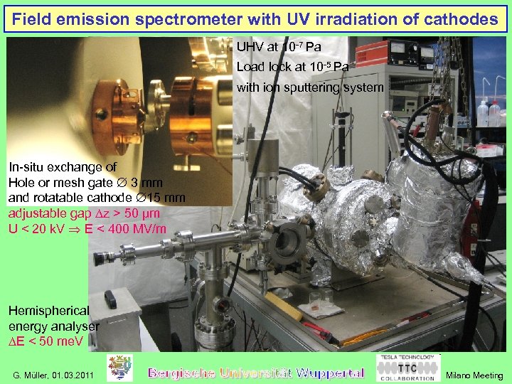 Field emission spectrometer with UV irradiation of cathodes UHV at 10 -7 Pa Load lock at 10 -5 Pa with ion sputtering system In-situ exchange of Hole or mesh gate 3 mm and rotatable cathode 15 mm adjustable gap Dz > 50 µm U < 20 k. V E < 400 MV/m Hemispherical energy analyser DE < 50 me. V G. Müller, 01. 03. 2011 Milano Meeting
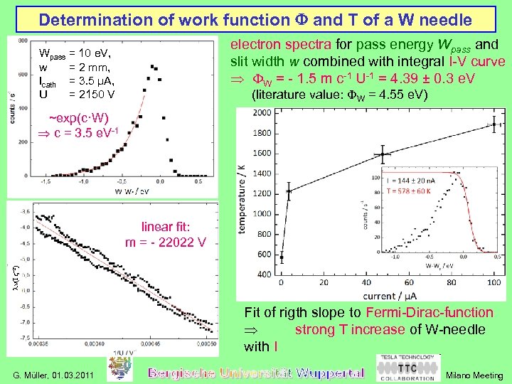 Determination of work function F and T of a W needle electron spectra for pass energy Wpass and slit width w combined with integral I-V curve FW = - 1. 5 m c-1 U-1 = 4. 39 ± 0. 3 e. V Wpass = 10 e. V, w = 2 mm, Icath = 3. 5 µA, U = 2150 V (literature value: FW = 4. 55 e. V) ~exp(c·W) c = 3. 5 e. V-1 ln(I V-2) linear fit: m = - 22022 V Fit of rigth slope to Fermi-Dirac-function strong T increase of W-needle with I G. Müller, 01. 03. 2011 Milano Meeting
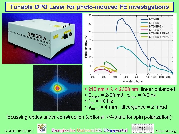 Tunable OPO Laser for photo-induced FE investigations • • 210 nm < l < 2300 nm, linear polarized Epulse = 2 -30 m. J, tpulse = 3 -5 ns frep = 10 Hz øbeam = 4 mm, divergence = 2 mrad focussing optics under construction (optional l/4 -plate for spin polarization) G. Müller, 01. 03. 2011 Milano Meeting
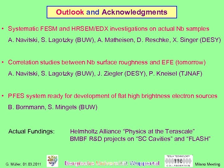 Outlook and Acknowledgments • Systematic FESM and HRSEM/EDX investigations on actual Nb samples A. Navitski, S. Lagotzky (BUW), A. Matheisen, D. Reschke, X. Singer (DESY) • Correlation studies between Nb surface roughness and EFE (tomorrow) A. Navitski, S. Lagotzky (BUW), J. Ziegler (DESY), P. Kneisel (TJNAF) • PFES system ready for development of flat high brightness electron sources B. Bornmann, S. Mingels (BUW) Actual Fundings: G. Müller, 01. 03. 2011 Helmholtz Alliance “Physics at the Terascale” BMBF R&D projects on “SC Cavities” and “FLASH” Milano Meeting


