afedfb9194928ef002c89cd66a6df8da.ppt
- Количество слайдов: 96

Reconfigurable Computation and Communication Architectures 조준동

발표순서 ë Why Reconfigurable System? ë S/W configurable platform의 필요성 ë Design Space of Reconfigurable Architectures ë New Taxonomy/Metric for RA ë Reconfigurable Radio and Multimedia Systems ë Network-centric Design: Clock and Power ë Reliable Design
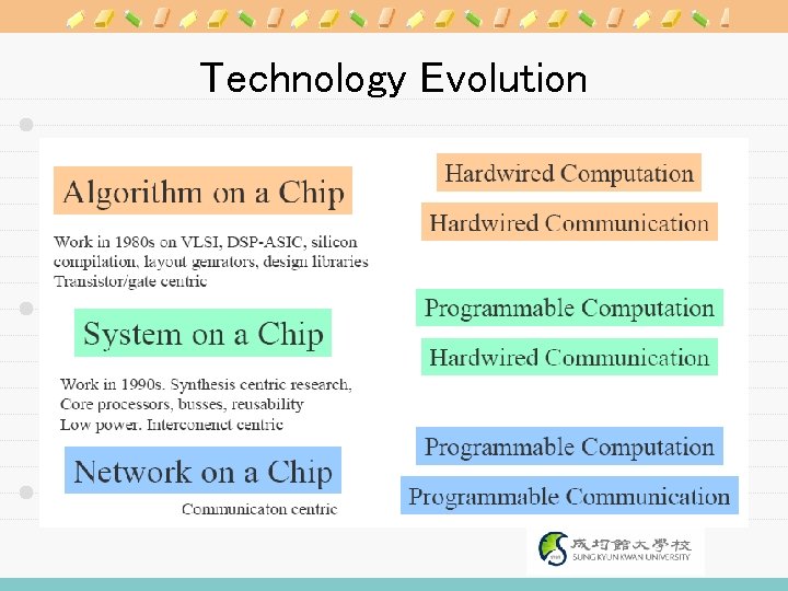
Technology Evolution
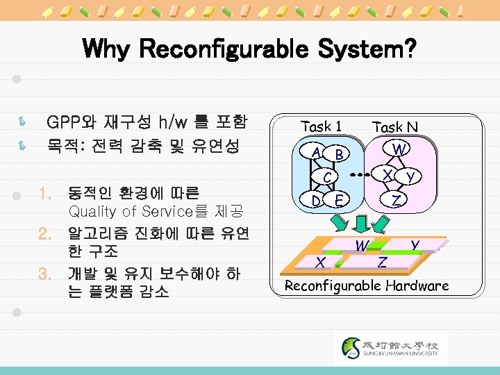
Why Reconfigurable System? ë GPP와 재구성 h/w 를 포함 ë 목적: 전력 감축 및 유연성 1. 동적인 환경에 따른 Quality of Service를 제공 2. 알고리즘 진화에 따른 유연 한 구조 3. 개발 및 유지 보수해야 하 는 플랫폼 감소 Task 1 Task N A B W C X Y D E Z X D H A W Y B I J C ZE Reconfigurable Hardware
Energy Efficiency of Reconfigurability system architecture communication protocol O/S and applications Partitioning of functions between wireless device and services on the network The mobiles must be flexible enough to accommodate a variety of multimedia services and communication capabilities and adapt to various operating conditions in an (energy) efficient way
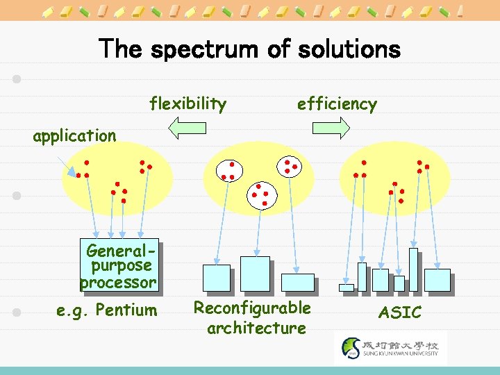
The spectrum of solutions flexibility efficiency application Generalpurpose processor e. g. Pentium Reconfigurable architecture ASIC
S/W configurable platform의 필요성 – – Doing More by Doing Less : 다양한 표준을 다룰 수 있는 능력이 필요 (AM, FM, GSM, UMTS, digital broadcasting standards, analog and digital television and other data links. A fully software reconfigurable multichannel broadband sampling receiver for standards in the 100 MHz band

Semiconductor Revolutions ’s Wave Makimoto software standard TTL 1957 custom “Mainstream Silicon Application is switching every 10 Years” n ctio s µproc. , nstru eam i memory str 1967 LSI, MSI hardware reconfigurable FPGAs 1977 ASICs, accel’s d ture n c stru desig I VLS sis st design cri 1 data ams stre 2007 1987 1997 coarse grain isis cr design 2 nd
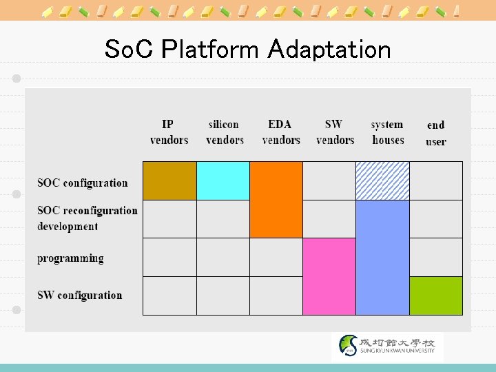
So. C Platform Adaptation
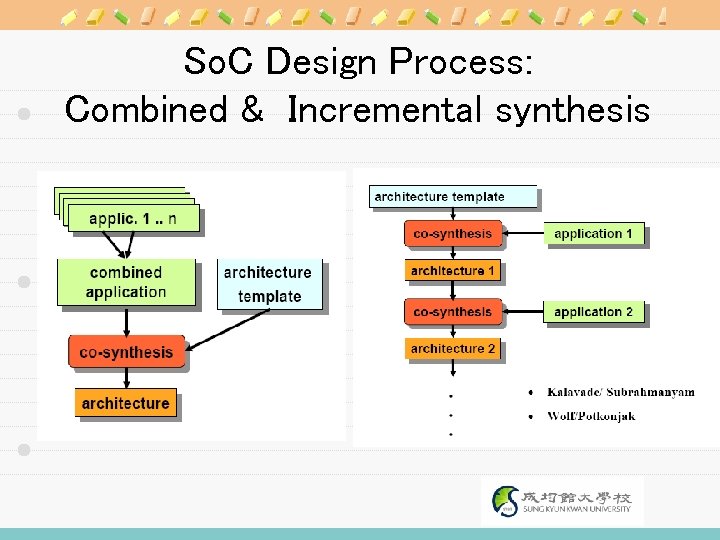
So. C Design Process: Combined & Incremental synthesis
Granularité de la reconfiguration Sébastien PILLEMENT - ENSSAT/LASTI ë Reconfiguration au niveau système Lx, C 62 (décomposition en cluster) ë Reconfiguration au niveau fonctionnel Pleiades, Ra. Pi. D, DART(2001) ë Reconfiguration au niveau opérateur Chameleon, Piperench, Morphosys(2000) ë Reconfiguration au niveau porte ë Napa, GARP, FPGA
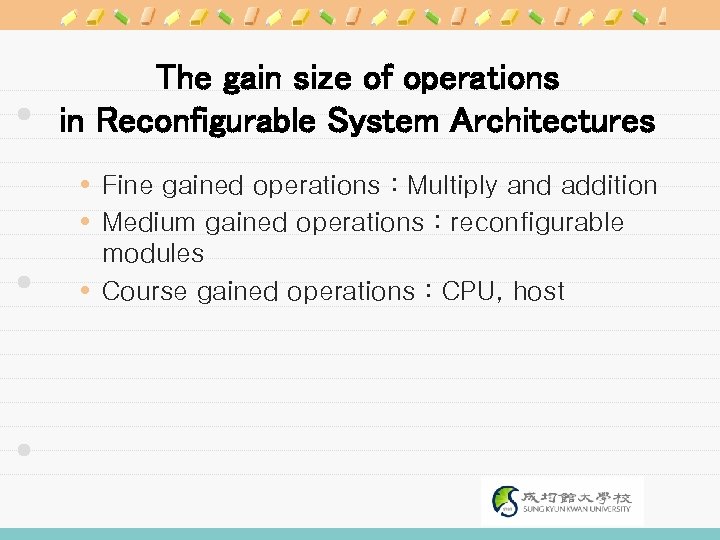
The gain size of operations in Reconfigurable System Architectures Fine gained operations : Multiply and addition Medium gained operations : reconfigurable modules Course gained operations : CPU, host
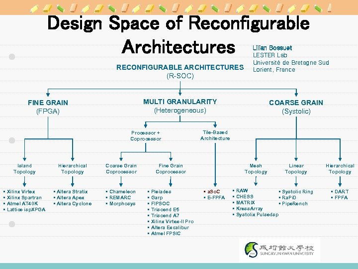
Design Space of Reconfigurable Architectures RECONFIGURABLE ARCHITECTURES (R-SOC) Lilian Bossuet LESTER Lab Université de Bretagne Sud Lorient, France MULTI GRANULARITY (Heterogeneous) FINE GRAIN (FPGA) Processor + Coprocessor Island Topology Hierarchical Topology Coarse Grain Coprocessor • Altera Stratix • Altera Apex • Altera Cyclone • Chameleon • REMARC • Morphosys • Pleiades • Garp • FIPSOC • Triscend E 5 • Triscend A 7 • Xilinx Virtex-II Pro • Altera Excalibur • Atmel FPSIC Tile-Based Architecture Fine Grain Coprocessor • Xilinx Virtex • Xilinx Spartran • Atmel AT 40 K • Lattice isp. XPGA COARSE GRAIN (Systolic) Mesh Topology • a. So. C • E-FPFA Linear Topology • RAW • Systolic Ring • CHESS • Ra. Pi. D • MATRIX • Pipe. Rench • Kress. Array • Systolix Pulsedsp Hierarchical Topology • DART • FPFA
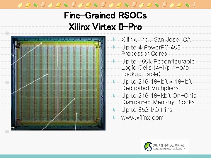
Fine-Grained RSOCs Xilinx Virtex II-Pro ë Xilinx, Inc. , San Jose, CA ë Up to 4 Power. PC 405 Processor Cores ë Up to 160 k Reconfigurable Logic Cells (4 -i/p 1 -o/p Lookup Table) ë Up to 216 18 -bit x 18 -bit Dedicated Multipliers ë Up to 216 18 -kbit On-Chip Distributed Memory Blocks ë Up to 852 I/O Pins ë www. xilinx. com
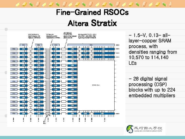
Fine-Grained RSOCs Altera Stratix - 1. 5 -V, 0. 13 - alllayer-copper SRAM process, with densities ranging from 10, 570 to 114, 140 LEs - 28 digital signal processing (DSP) blocks with up to 224 embedded multipliers

Digital Signal Processing With FPGAs Paul Ekas Jean-Charles Bouzigues
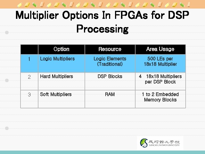
Multiplier Options In FPGAs for DSP Processing Option Resource Area Usage 1 Logic Multipliers Logic Elements (Traditional) 500 LEs per 18 x 18 Multiplier 2 Hard Multipliers DSP Blocks 4 18 x 18 Multipliers per DSP Block 3 Soft Multipliers RAM 1 to 2 Embedded Memory Blocks
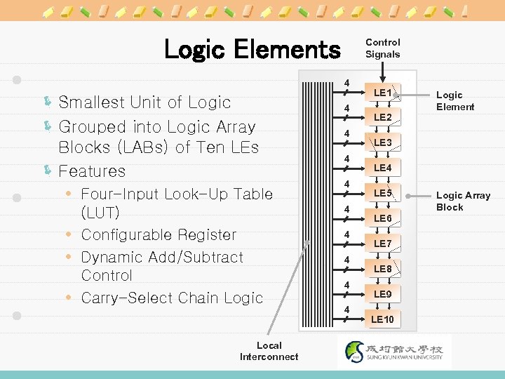
Logic Elements Control Signals 4 ë Smallest Unit of Logic ë Grouped into Logic Array Blocks (LABs) of Ten LEs ë Features Four-Input Look-Up Table (LUT) Configurable Register Dynamic Add/Subtract Control Carry-Select Chain Logic Local Interconnect 4 4 4 4 4 LE 1 LE 2 Logic Element LE 3 LE 4 LE 5 LE 6 LE 7 LE 8 LE 9 LE 10 Logic Array Block
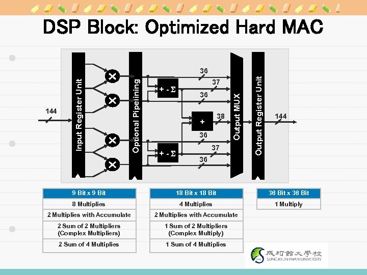
DSP Block: Optimized Hard MAC 36 38 + 36 +-S 37 36 Output Register Unit +-S 37 Output MUX Optional Pipelining 144 Input Register Unit 36 144 9 Bit x 9 Bit 18 Bit x 18 Bit 36 Bit x 36 Bit 8 Multiplies 4 Multiplies 1 Multiply 2 Multiplies with Accumulate 2 Sum of 2 Multipliers (Complex Multipliers) 1 Sum of 2 Multipliers (Complex Multiply) 2 Sum of 4 Multiplies 1 Sum of 4 Multiplies
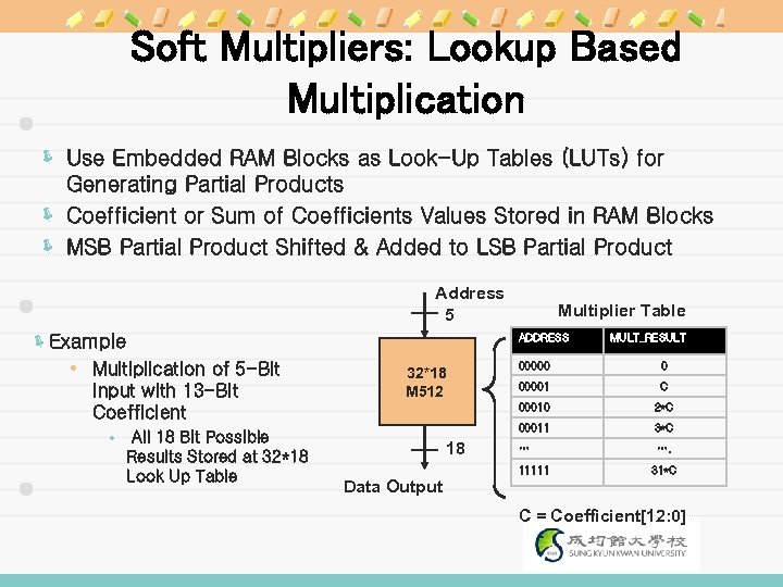
Soft Multipliers: Lookup Based Multiplication ë Use Embedded RAM Blocks as Look-Up Tables (LUTs) for Generating Partial Products ë Coefficient or Sum of Coefficients Values Stored in RAM Blocks ë MSB Partial Product Shifted & Added to LSB Partial Product Address 5 ëExample ADDRESS Multiplication of 5 -Bit Input with 13 -Bit Coefficient Multiplier Table All 18 Bit Possible Results Stored at 32*18 Look Up Table MULT_RESULT 0 00001 C 2*C 00011 18 00000 00010 32*18 M 512 3*C … …. 11111 31*C Data Output C = Coefficient[12: 0]
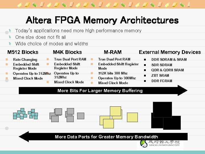
Altera FPGA Memory Architectures ë Today’s applications need more high performance memory ë One size does not fit all ë Wide choice of modes and widths M 512 Blocks n n M 4 K Blocks n Rate Changing n Embedded Shift Register Mode n Operates Up to 312 Mhz Mixed Clock Mode n True Dual Port RAM Embedded Shift Register Mode Operates Up to 312 Mhz Mixed Clock Mode M-RAM n n n External Memory Devices True Dual Port RAM Embedded Shift Register Mode 512 K bits 300 Mhz Operates Up to 300 Mhz Mixed Clock Mode n DDR SDRAM & SRAM n SDRAM n QDR & QDRII SRAM n ZBT SRAM n DDR FCRAM More Bits For Larger Memory Buffering More Data Ports for Greater Memory Bandwidth

Soft Multiplier: Sum of Multiplications 16 -Bit Serial Shift Registers Input 1 1 (Sample 16 -Bit, Coefficient 16 Bit) 1 Sum of Multiplications Table M 512 32*18 18 + 19 35 + Example: FIR Filter Memory: 2 M 512 Output M 512 32*18 18 MULT_RESULT 0000 0 C 0 0010 C 1 0011 C 0+C 1 … 4 ADDRESS 0001 4 …. 1111 C 0+C 1+C 2+C 3

Example Direct Sequence Spread Spectrum (DSSS) Modem
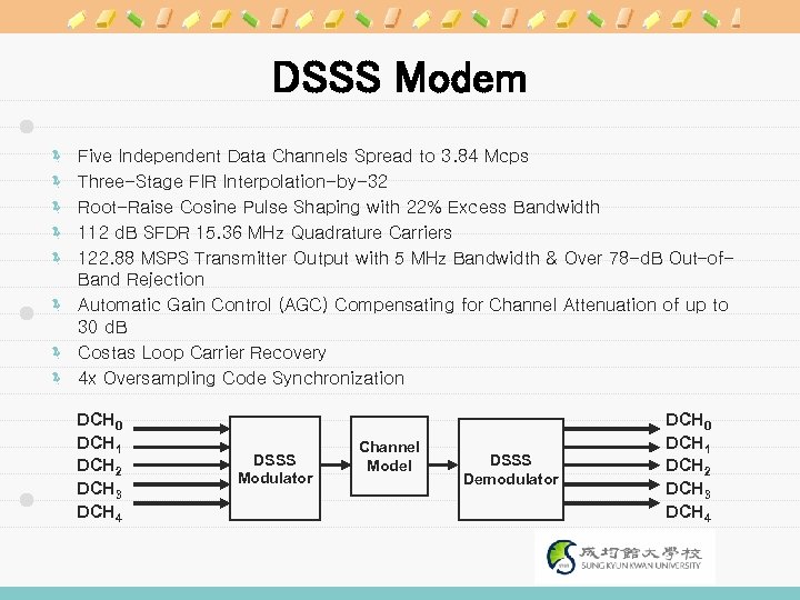
DSSS Modem Five Independent Data Channels Spread to 3. 84 Mcps Three-Stage FIR Interpolation-by-32 Root-Raise Cosine Pulse Shaping with 22% Excess Bandwidth 112 d. B SFDR 15. 36 MHz Quadrature Carriers 122. 88 MSPS Transmitter Output with 5 MHz Bandwidth & Over 78 -d. B Out–of. Band Rejection ë Automatic Gain Control (AGC) Compensating for Channel Attenuation of up to 30 d. B ë Costas Loop Carrier Recovery ë 4 x Oversampling Code Synchronization ë ë ë DCH 0 DCH 1 DCH 2 DCH 3 DCH 4 DSSS Modulator Channel Model DSSS Demodulator DCH 0 DCH 1 DCH 2 DCH 3 DCH 4
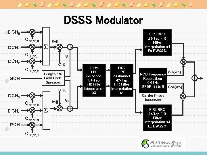
DSSS Modulator DCH 0 Cch, 16, 0 DCH 1 S FIR 3 RRC 25 -Tap FIR Filter Interpolation x 4 Ex BW: 22% Re[] Cch, 16, 1 gi DCH 2 K Cch, 16, 2 SCH Length 256 Gold Code Spreader K DCH 3 Cch, 16, 8 DCH 4 Cch, 16, 9 PCH Cch, 16, 10 Im[] S gq FIR 1 LPF 2 -Channel 87 -Tap FIR Filter Interpolation x 2 FIR 2 LPF 2 -Channel 47 -Tap FIR Filter Interpolation x 4 Sin(wn) NCO Frequency Resolution: 0. 03 Hz SFDR: 112 d. B Cos(wn) Carrier Phase Increment FIR 3 RRC 25 -Tap FIR Filter Interpolation x 4 Ex BW: 22%
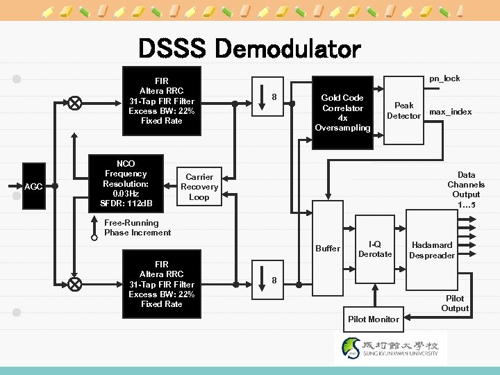
DSSS Demodulator FIR Altera RRC 31 -Tap FIR Filter Excess BW: 22% Fixed Rate AGC NCO Frequency Resolution: 0. 03 Hz SFDR: 112 d. B pn_lock 8 Gold Code Correlator 4 x Oversampling Peak Detector max_index Data Channels Output 1… 5 Carrier Recovery Loop Free-Running Phase Increment Buffer FIR Altera RRC 31 -Tap FIR Filter Excess BW: 22% Fixed Rate I-Q Derotate Hadamard Despreader 8 Pilot Output Pilot Monitor
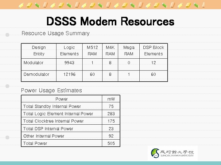
DSSS Modem Resources Resource Usage Summary Design Entity Logic Elements M 512 RAM M 4 K RAM Mega RAM DSP Block Elements Modulator 9943 1 8 0 12 Demodulator 12196 60 8 1 60 Power Usage Estimates Power m. W Total Standby Internal Power 75 Total Logic Element Internal Power 283 Total Clocktree Internal Power 175 Total DSP Internal Power 23 Other Internal Power 92 Total Power 505
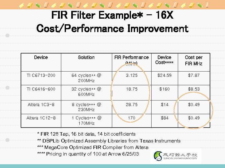
FIR Filter Example* – 16 X Cost/Performance Improvement Device Solution FIR Performance (MHz) Device Cost**** Cost per FIR MHz TI C 6713 -200 64 cycles** @ 200 MHz 3. 125 $24. 59 $7. 87 TI C 6416 -600 32 cycles** @ 600 MHz 18. 75 $160 $8. 53 Altera 1 C 3 -8 8 cycles*** @ 230 MHz 28. 75 $14 $0. 49 Altera 1 C 12 -8 1 Cycles*** @ 170 MHz 170 $84 $0. 49 * FIR 128 Tap, 16 bit data, 14 bit coefficients ** DSPLib Optimized Assembly Libraries from Texas Instruments *** Mega. Core Optimized FIR Compiler from Altera **** Pricing in quantity of 100 at Arrow 6/25/03
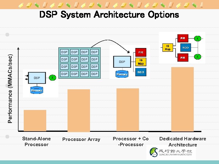
DSP System Architecture Options Performance (MMACs/sec) DSP DSP DSP DSP DSP Stand-Alone Processor Array Processor + Co -Processor Dedicated Hardware Architecture
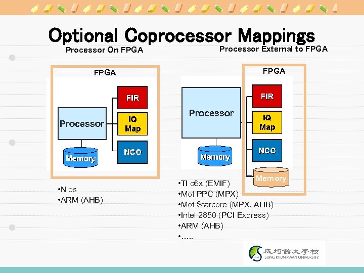
Optional Coprocessor Mappings Processor On FPGA Processor External to FPGA Processor • Nios • ARM (AHB) Memory • TI c 6 x (EMIF) • Mot PPC (MPX) • Mot Starcore (MPX, AHB) • Intel 2850 (PCI Express) • ARM (AHB) • …. .
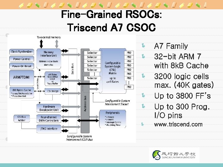
Fine-Grained RSOCs: Triscend A 7 CSOC ë A 7 Family ë 32 -bit ARM 7 with 8 k. B Cache ë 3200 logic cells max. (40 K gates) ë Up to 3800 FF’s ë Up to 300 Prog. I/O pins ë www. triscend. com
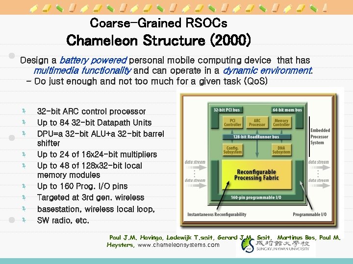
Coarse-Grained RSOCs Chameleon Structure (2000) Design a battery powered personal mobile computing device that has multimedia functionality and can operate in a dynamic environment. - Do just enough and not too much for a given task (Qo. S) ë ë ë ë ë 32 -bit ARC control processor Up to 84 32 -bit Datapath Units DPU=a 32 -bit ALU+a 32 -bit barrel shifter Up to 24 of 16 x 24 -bit multipliers Up to 48 of 128 x 32 -bit local memory modules Up to 160 Prog. I/O pins Targeted at 3 rd gen. wireless basestation, wireless local loop, SW radio, etc. Paul J. M. Havinga, Lodewijk T. smit, Gerard J. M. Smit, Martinus Bos, Paul M. Heysters, www. chameleonsystems. com
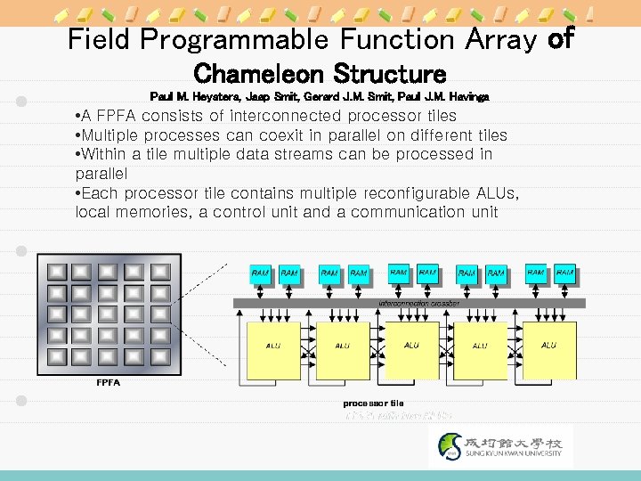
Field Programmable Function Array of Chameleon Structure Paul M. Heysters, Jaap Smit, Gerard J. M. Smit, Paul J. M. Havinga • A FPFA consists of interconnected processor tiles • Multiple processes can coexit in parallel on different tiles • Within a tile multiple data streams can be processed in parallel • Each processor tile contains multiple reconfigurable ALUs, local memories, a control unit and a communication unit
Field Programmable Function Array ëThe FPFA concept has a number of advantage The FPFA has a highly regular organisation We use general purpose process core Its scalability stands in contrast to the dedicated chips designed nowadays The FPFA can do media processing tasks such as compression/decompression efficiently
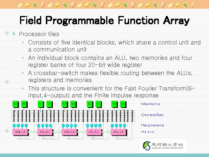
Field Programmable Function Array ë Processor tiles Consists of five identical blocks, which share a control unit and a communication unit An individual block contains an ALU, two memories and four register banks of four 20 -bit wide register A crossbar-switch makes flexible routing between the ALUs, registers and memories This structure is convenient for the Fast Fourier Transform(6 input, 4 -output) and the Finite impulse response
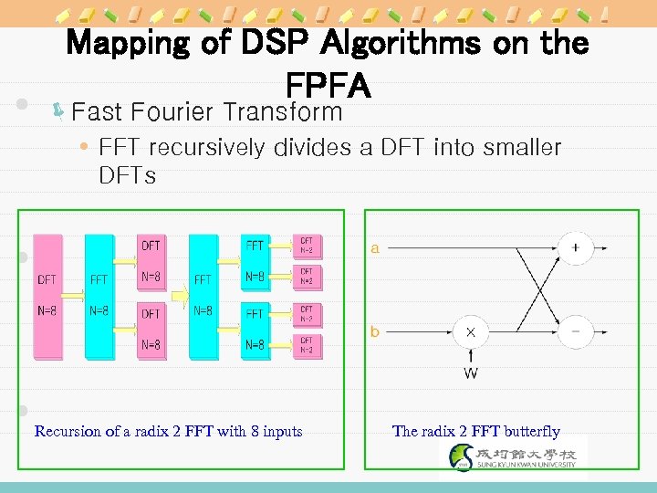
Mapping of DSP Algorithms on the FPFA ëFast Fourier Transform FFT recursively divides a DFT into smaller DFTs Recursion of a radix 2 FFT with 8 inputs The radix 2 FFT butterfly
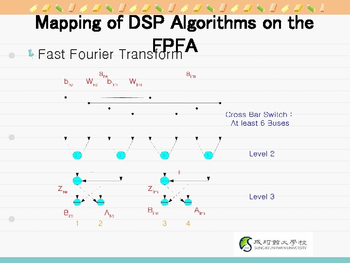
Mapping of DSP Algorithms on the FPFA ëFast Fourier Transform

Mapping of DSP Algorithms on the FPFA ëFive-tap finite-impulse response filter
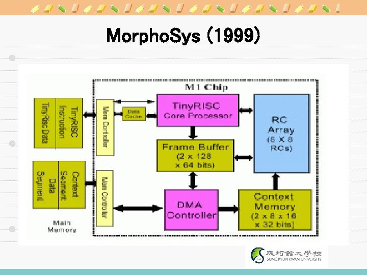
Morpho. Sys (1999)
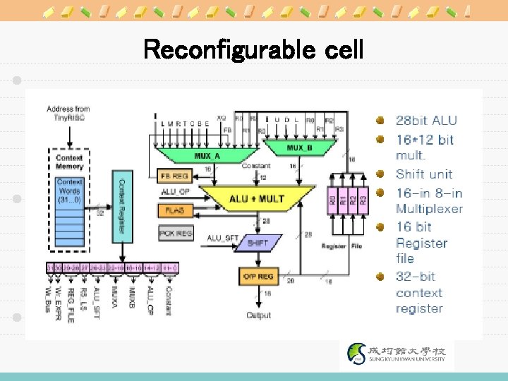
Reconfigurable cell
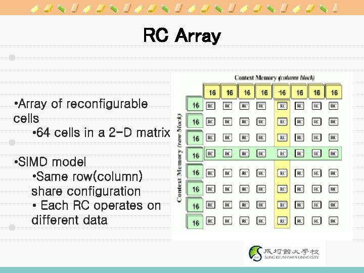
RC Array • Array of reconfigurable cells • 64 cells in a 2 -D matrix • SIMD model • Same row(column) share configuration • Each RC operates on different data
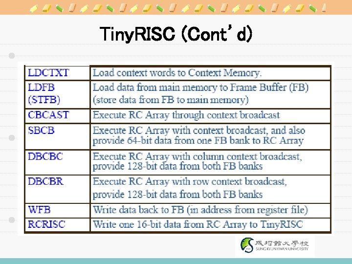
Tiny. RISC (Cont’d)

Implementation & Performance • 0. 35 micron technology • 4 metal layers • Operation at 100 MHz • 170 mm 2 Motion Estimation Block size : 16 x 16 pixel, Image size : 352 x 288 pixel
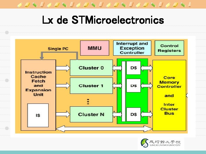
Lx de STMicroelectronics
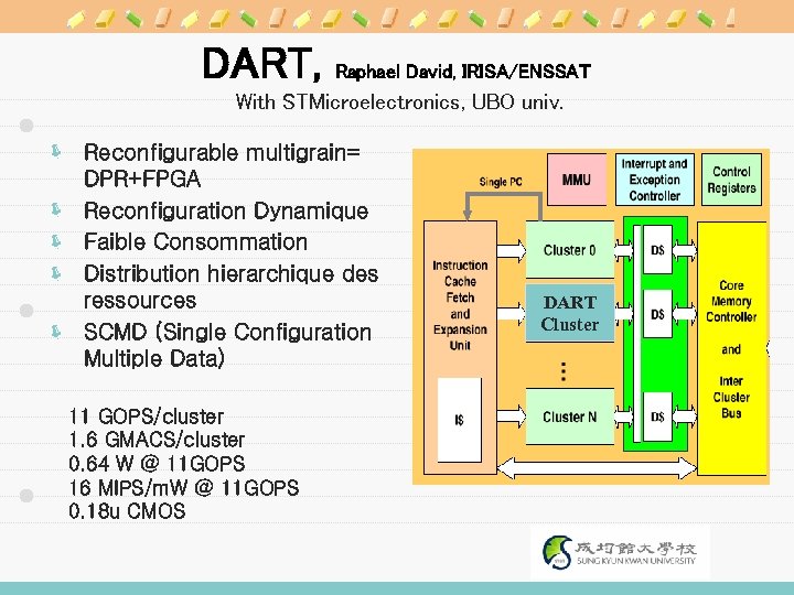
DART, Raphael David, IRISA/ENSSAT With STMicroelectronics, UBO univ. ë Reconfigurable multigrain= DPR+FPGA ë Reconfiguration Dynamique ë Faible Consommation ë Distribution hierarchique des ressources ë SCMD (Single Configuration Multiple Data) 11 GOPS/cluster 1. 6 GMACS/cluster 0. 64 W @ 11 GOPS 16 MIPS/m. W @ 11 GOPS 0. 18 u CMOS DART Cluster

Cluster architecture DPR 1 Control DPR 4 DMA ctrl Config mem. DPR 3 DPR 5 FPGA DPR 6 Segmented network DPR 2 Data mem
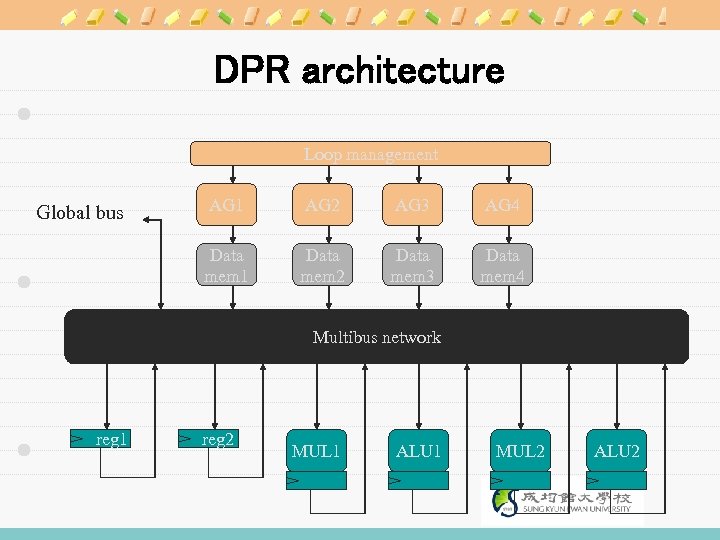
DPR architecture Loop management AG 1 AG 2 AG 3 AG 4 Data mem 1 Global bus Data mem 2 Data mem 3 Data mem 4 Multibus network reg 1 reg 2 MUL 1 ALU 1 MUL 2 ALU 2
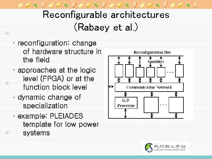
Reconfigurable architectures (Rabaey et al. ) · reconfiguration: change of hardware structure in the field · approaches at the logic level (FPGA) or at the function block level · dynamic change of specialization · example: PLEIADES template for low power systems
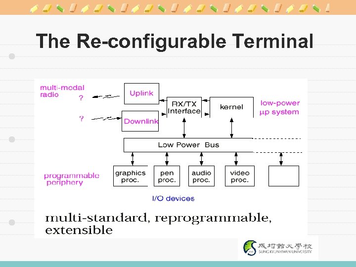
The Re-configurable Terminal
Satellite Processors
Elements of Energy- Efficiency
Communication Network

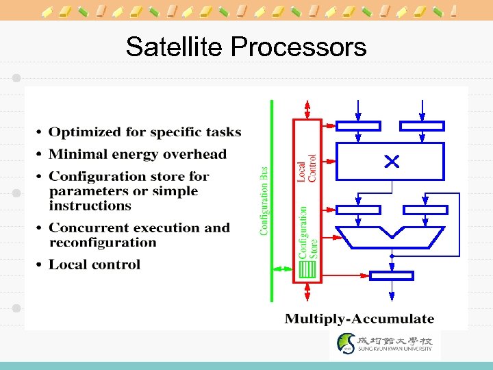
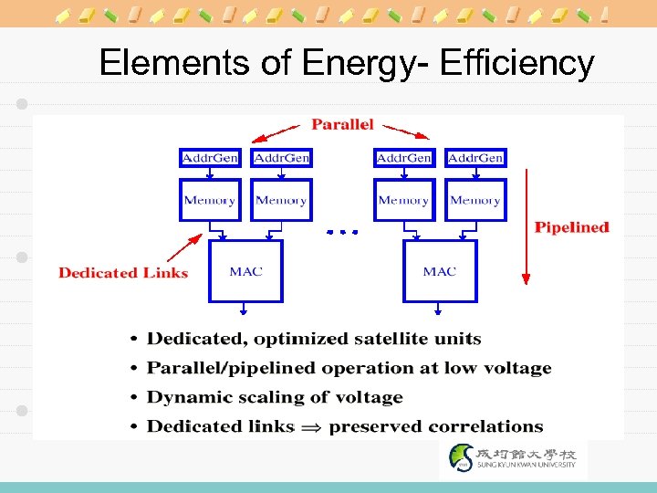
Distributed Data- Driven Control Execution of a hardware module is triggered by the arrival of tokens. When there are no tokens to be processed at a given module, no switching activity occurs in that module.
Design Methodology
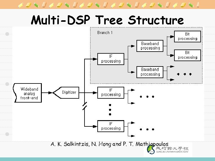
Multi-DSP Tree Structure A. K. Salkintzis, N. Hong and P. T. Mathiopoulos
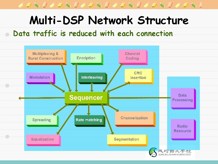
Multi-DSP Network Structure Data traffic is reduced with each connection
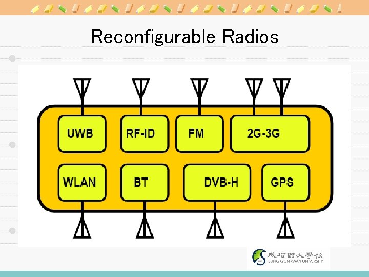
Reconfigurable Radios
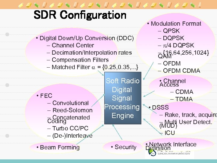
SDR Configuration • Digital Down/Up Conversion (DDC) – Channel Center – Decimation/Interpolation rates – Compensation Filters – Matched Filter a = {0. 25, 0. 35, . . . } • FEC – Convolutional – Reed-Solomon – Concatenated Coding – Turbo CC/PC – (De-)Interleave • Beam Forming Soft Radio Digital Signal Processing Engine • Security • Modulation Format – QPSK – DQPSK – p/4 DQPSK – {16, 64, 256, 1024} QAM – OFDM CDMA • Channel Access – CDMA – TDMA • DSSS – Rake, track, acquire – Multi User Detect. (MUD) – ICU • Network Interface Definition
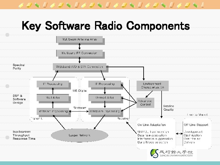
Key Software Radio Components
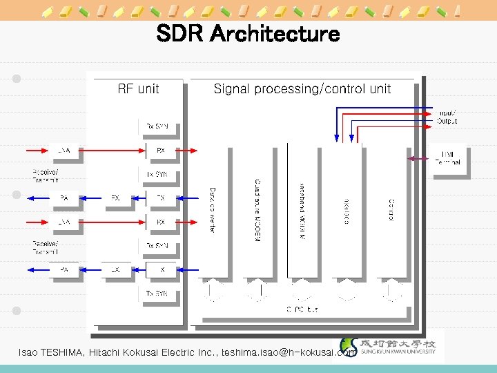
SDR Architecture Isao TESHIMA, Hitachi Kokusai Electric Inc. , teshima. isao@h-kokusai. com
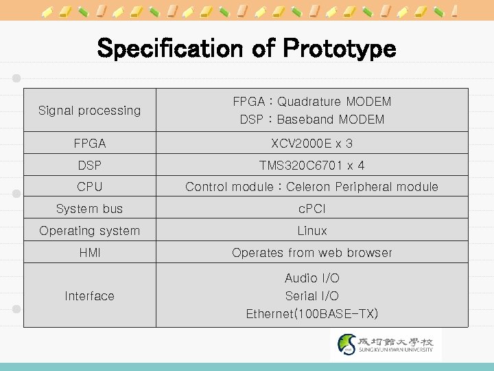
Specification of Prototype Signal processing FPGA : Quadrature MODEM DSP : Baseband MODEM FPGA XCV 2000 E x 3 DSP TMS 320 C 6701 x 4 CPU Control module : Celeron Peripheral module System bus c. PCI Operating system Linux HMI Operates from web browser Interface Audio I/O Serial I/O Ethernet(100 BASE-TX)
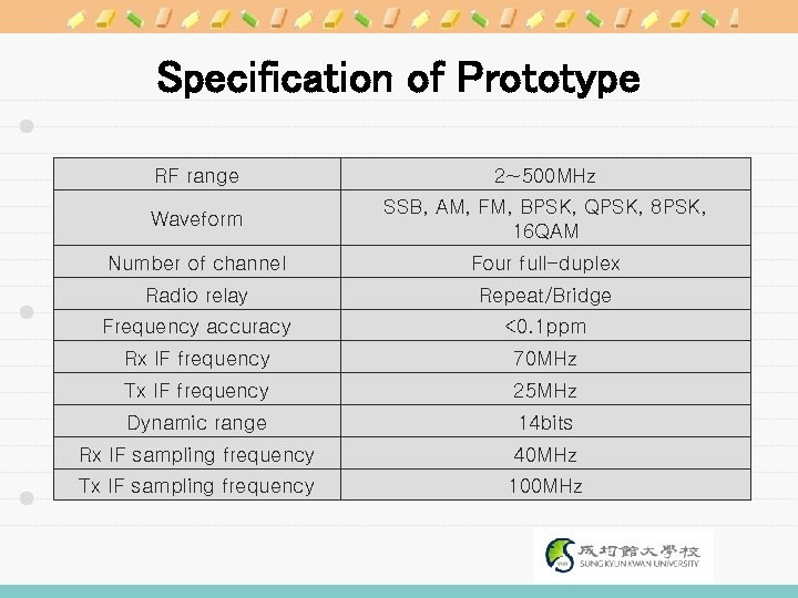
Specification of Prototype RF range 2~500 MHz Waveform SSB, AM, FM, BPSK, QPSK, 8 PSK, 16 QAM Number of channel Four full-duplex Radio relay Repeat/Bridge Frequency accuracy <0. 1 ppm Rx IF frequency 70 MHz Tx IF frequency 25 MHz Dynamic range 14 bits Rx IF sampling frequency 40 MHz Tx IF sampling frequency 100 MHz
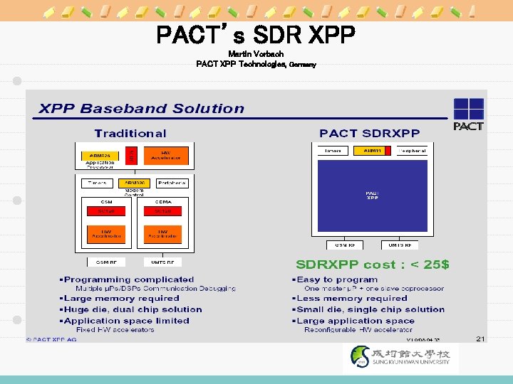
PACT’s SDR XPP Martin Vorbach PACT XPP Technologies, Germany
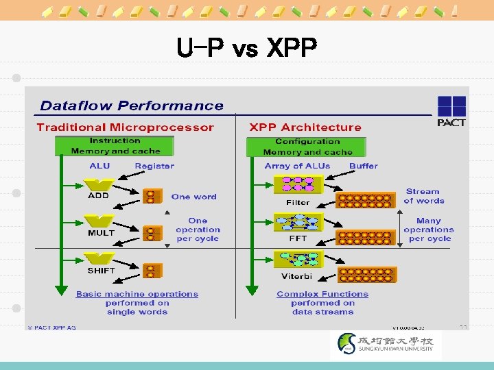
U-P vs XPP
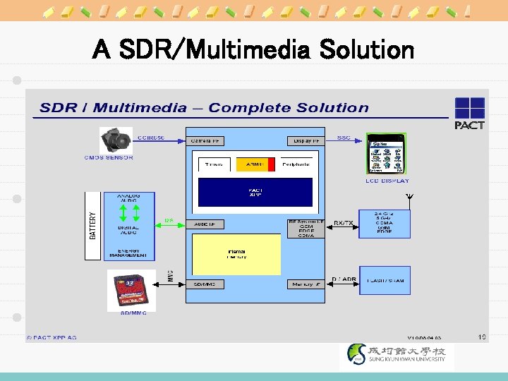
A SDR/Multimedia Solution
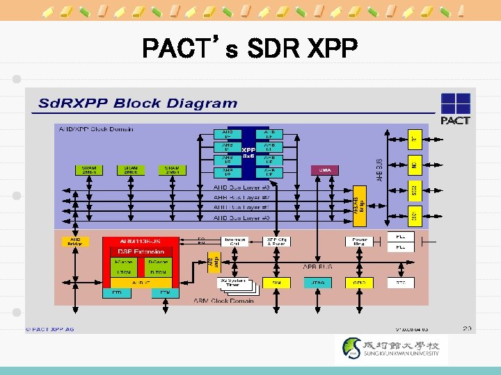
PACT’s SDR XPP
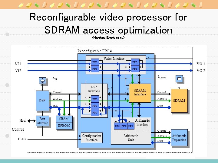
Reconfigurable video processor for SDRAM access optimization (Henriss, Ernst et al. )

Reconfigurable video platform · SDRAM memory centered design · FPGA based scheduler merges different streams and random accesses exploitation of SDRAM bank structure · supports 2 HDTV streams at 1. 48 Gbit/s each plus DSP and filter unit access · reaches 700 MByte/s in practical application for 4 Byte SDRAM memory word · extremly cost efficient design · used in professional video product line
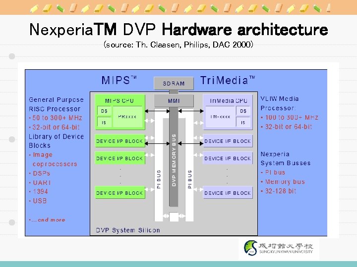
Nexperia. TM DVP Hardware architecture (source: Th. Claasen, Philips, DAC 2000)
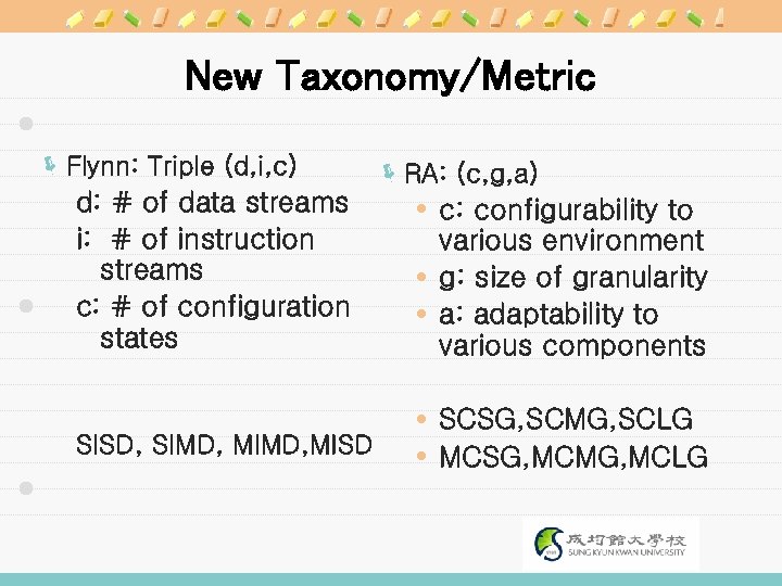
New Taxonomy/Metric ë Flynn: Triple (d, i, c) d: # of data streams i: # of instruction streams c: # of configuration states SISD, SIMD, MISD ë RA: (c, g, a) c: configurability to various environment g: size of granularity a: adaptability to various components SCSG, SCMG, SCLG MCSG, MCMG, MCLG
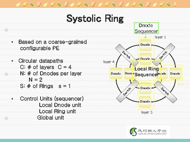
Systolic Ring Dnode Sequencer layer 1 • Based on a coarse-grained configurable PE Dnode it h Dnode layer 4 Local Ring Dnode Sequencer Dnode h Dnode Sw it c • Circular datapaths C: # of layers C = 4 N: # of Dnodes per layer N=2 S: # of Rings s = 1 ch it c • Control Units (sequencer) Local Dnode unit Local Ring unit Global unit Sw Sw Dnode layer 3 Dnode Sw layer 2 it ch
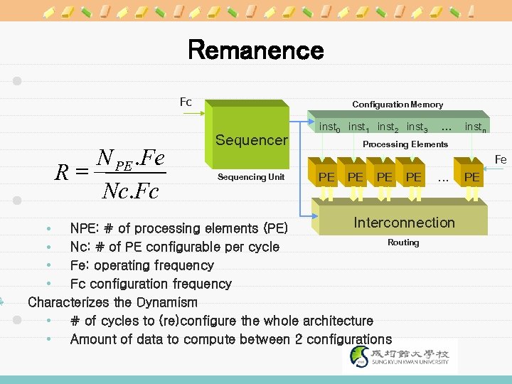
ë Remanence Fc N PE. Fe R= Nc. Fc Configuration Memory Sequencer inst 0 inst 1 inst 2 inst 3 … inst n Processing Elements Fe Sequencing Unit PE PE … Interconnection NPE: # of processing elements (PE) Routing Nc: # of PE configurable per cycle Fe: operating frequency Fc configuration frequency Characterizes the Dynamism # of cycles to (re)configure the whole architecture Amount of data to compute between 2 configurations PE
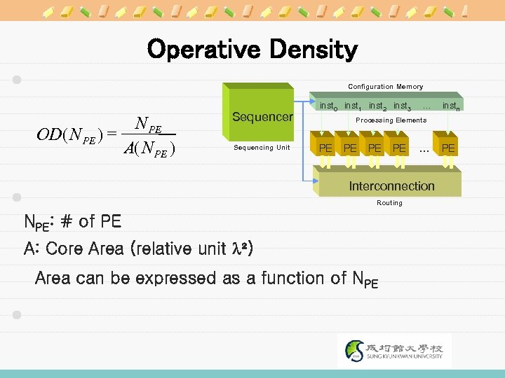
Operative Density Configuration Memory N PE OD( N PE ) = A( N PE ) Sequencer Sequencing Unit inst 0 inst 1 inst 2 inst 3 … instn Processing Elements PE PE … Interconnection Routing NPE: # of PE A: Core Area (relative unit ²) Area can be expressed as a function of NPE PE
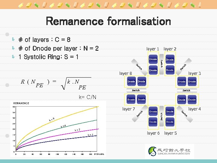
Remanence formalisation ë # of layers : C = 8 ë # of Dnode per layer : N = 2 ë 1 Systolic Ring: S = 1 layer 2 layer 8 R (N PE ) = layer 3 k. N PE k= C/N REMANENCE 40 layer 7 layer 4 35 30 k= 8 25 k= 4 20 k=2 layer 6 k=1 15 10 5 0 0 20 40 60 80 100 120 140 160 180 # Dnodes layer 5
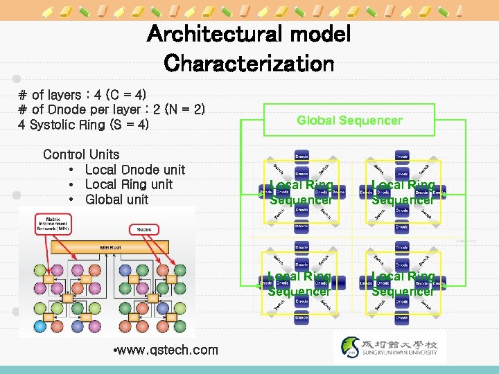
Architectural model Characterization # of layers : 4 (C = 4) # of Dnode per layer : 2 (N = 2) 4 Systolic Ring (S = 4) Control Units • Local Dnode unit • Local Ring unit • Global unit Global Sequencer Local Ring Sequencer • www. qstech. com Local Ring Sequencer
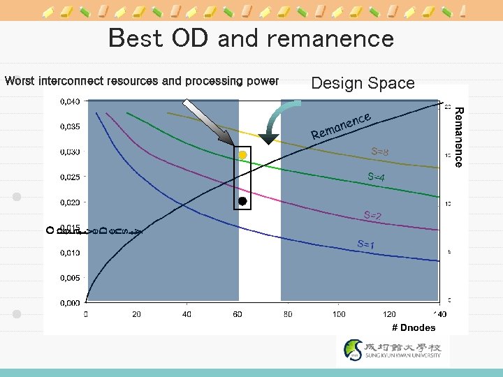
Best OD and remanence Worst interconnect resources and processing power Design Space

Worst OD and remanence Best interconnect resources and processing power Design Space
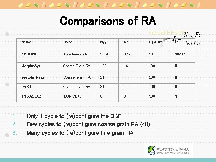
Comparisons of RA Pascal BENOIT Name Type NPE Nc F (MHz) R ARDOISE Fine Grain RA 2304 0. 14 33 16457 Morpho. Sys Coarse Grain RA 128 16 100 8 Systolic Ring Coarse Grain RA 24 4 200 6 DART Coarse Grain RA 24 4 130 6 8 8 300 1 TMS 320 C 62 DSP VLIW 1. 2. Only 1 cycle to (re)configure the DSP 3. Many cycles to (re)configure fine grain RA Few cycles to (re)configure coarse grain RA ( 8)
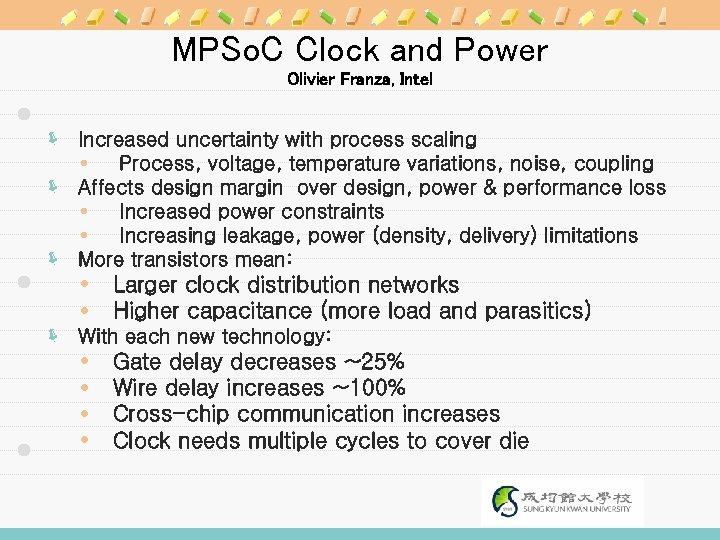
MPSo. C Clock and Power Olivier Franza, Intel ë Increased uncertainty with process scaling Process, voltage, temperature variations, noise, coupling ë Affects design margin over design, power & performance loss Increased power constraints Increasing leakage, power (density, delivery) limitations ë More transistors mean: Larger clock distribution networks Higher capacitance (more load and parasitics) ë With each new technology: Gate delay decreases ~25% Wire delay increases ~100% Cross-chip communication increases Clock needs multiple cycles to cover die
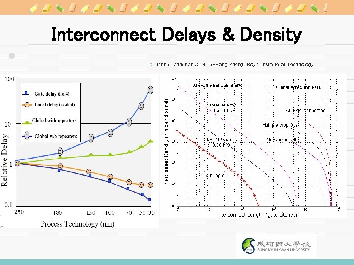
Interconnect Delays & Density ëHannu Tenhunen & Dr. Li-Rong Zheng, Royal Institute of Technology
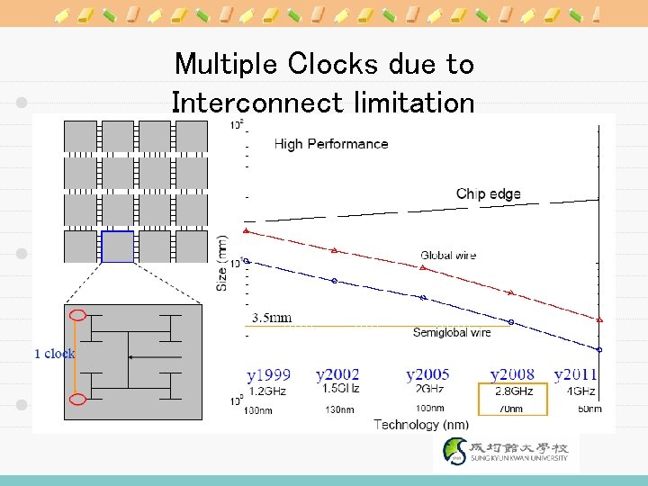
Multiple Clocks due to Interconnect limitation
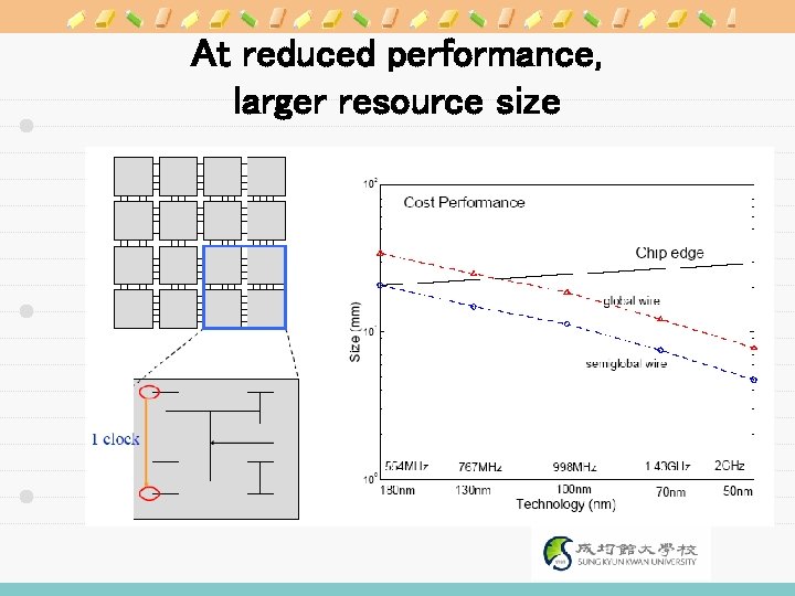
At reduced performance, larger resource size
Noise in Mixed Signal Systems
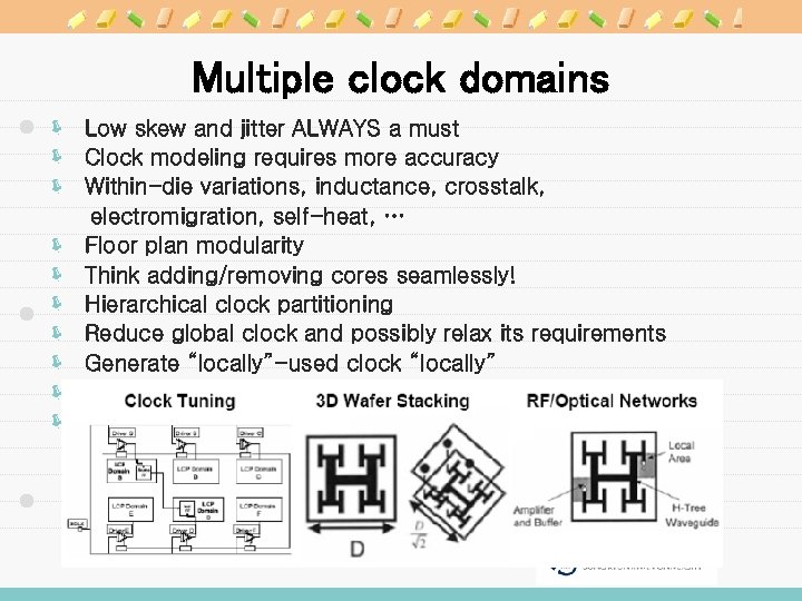
Multiple clock domains ë Low skew and jitter ALWAYS a must ë Clock modeling requires more accuracy ë Within-die variations, inductance, crosstalk, electromigration, self-heat, … ë Floor plan modularity ë Think adding/removing cores seamlessly! ë Hierarchical clock partitioning ë Reduce global clock and possibly relax its requirements ë Generate “locally”-used clock “locally” ë Implement clock domain deskewing techniques ë Bound clock problem into simple, reliable, efficient domains
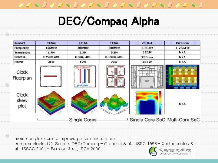
DEC/Compaq Alpha more complex core to improve performance, more complex clocks (? ), Source: DEC/Compaq – Gronoski & al. , JSSC 1998 – Xanthopoulos & al. , ISSCC 2001 – Barroso & al. , ISCA 2000
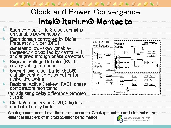
Clock and Power Convergence Intel® Itanium® Montecito ë Each core split into 3 clock domains on variable power supply ë Each domain controlled by Digital Frequency Divider (DFD) generating low-skew variablefrequency clocks; fed by central PLL and aligned through phase detectors ë Regional Voltage Detector (RVD): supply voltage monitor ë Second level clock buffer (SLCB): digitally controlled delay buffer for active deskewing ë Regional Active Deskew (RAD): phase comparators monitoring and adjusting delay difference between SLCBs ë Clock Vernier Device (CVD): digitally controlled delay buffer Clock generation and distribution are essential enablers of microprocessor performance
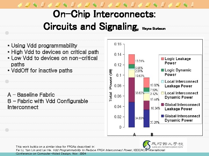
On-Chip Interconnects: Circuits and Signaling, Wayne Burleson • Using Vdd programmability • High Vdd to devices on critical path • Low Vdd to devices on non-critical paths • Vdd. Off for inactive paths A – Baseline Fabric B – Fabric with Vdd Configurable Interconnect This work builds on a similar idea for FPGAs described in: Fei Li, Yan Lin and Lei He. Vdd Programmability to Reduce FPGA Interconnect Power, IEEE/ACM International Conference on Computer-Aided Design, Nov. 2004
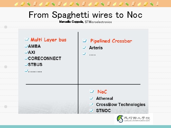
From Spaghetti wires to Noc Marcello Coppola, STMicroelectronics

Benchmarks, EE Times, 7/2005 ë Xpipes, Bologna and Stanford : compared w/ Amba AHB multilayer bus, 21% faster, but worse latency ë When, Univ. of Kaiserslautern: LPDC decoder: 500 Mhz vs 64 Mhz (fixed bus), but 30 W vs. 700 m. W, twice the die size. ë Arteris: better die size, comparable power consumption, 740 Mhz (250 Mhz) ë Sonics. MX: power-efficient mobile-handset w/ power management ë STNo. C, Spidergon: topology w/ degree 2 -3
No. C Applications http: //www. eit. uni-kl. de/wehn • Turbo-Decoder UMTS compliant, 100 Mbit: large flexibilty w/ 14 parallel units, area = 16. 84 mm 2 (14 mm 2 PUs, 2. 8 mm 2 No. C) • LDPC Decoding, T. Theocharides, G. Link, N. Chip, T. Theocharides, G. Link, N. Vijaykrishnan, M. J. Irwin, Int. Conference on VLSI Design 2005 – 1024 Bit block size, 1. 2 Gb/s, R=0. 75 – No. C: 5 x 5 2 D mesh, dimension-order routing, large flexibility – 160 nm CMOS Technology, 1. 8 V, 500 MHz, 110 mm 2, ~30 Watt
Reliable design, G. De Micheli 1. Manufacturing imperfections: More likely to happen as lithography scales down 2. Approximations during design: Uncertainty about details of design 3. Aging: Oxide breakdown, electromigration 4. Environment-induced Soft-errors (Data corruption due external radiation exposure), electro-magnetic interference 5. Operating-mode induced: Extremely-low voltage supply
Dealing with variability • Most variability problems that induce timing errors 1. 2. 3. 4. Power supply variation Wire length estimation Crosstalk Soft errors
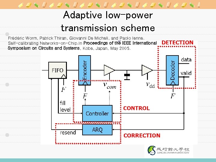
Adaptive low-power transmission scheme Frédéric Worm, Patrick Thiran, Giovanni De Micheli, and Paolo Ienne. Self-calibrating Networks-on-Chip. In Proceedings of the IEEE International Symposium on Circuits and Systems, Kobe, Japan, May 2005.
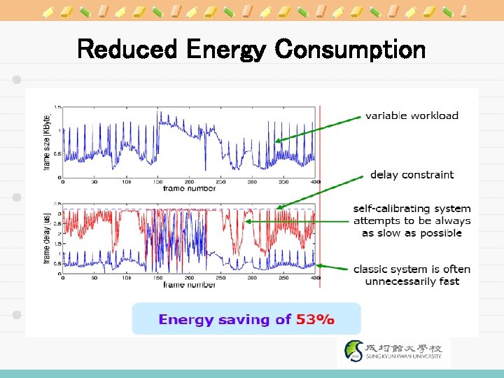
Reduced Energy Consumption
afedfb9194928ef002c89cd66a6df8da.ppt