fd9d596579e5623f1a808c51bd82e18d.ppt
- Количество слайдов: 86
 Putting it all together — Chip Level Issues © Digital Integrated Circuits 2 nd and F. Brewer Interconnect
 Full Chip Issues Noise Power Distribution Clocking Packaging Pads © Digital Integrated Circuits 2 nd and F. Brewer Interconnect
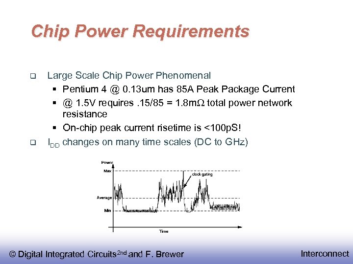 Chip Power Requirements Large Scale Chip Power Phenomenal § Pentium 4 @ 0. 13 um has 85 A Peak Package Current § @ 1. 5 V requires. 15/85 = 1. 8 m. W total power network resistance § On-chip peak current risetime is <100 p. S! IDD changes on many time scales (DC to GHz) © Digital Integrated Circuits 2 nd and F. Brewer Interconnect
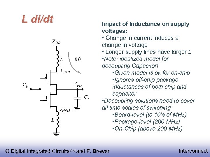
 Power Coupled Noise Droop due to IR drop, Ld. I/dt noise and Supply Inductance Modulates behavior of Gates § § § Signalling Failure Reduction of Noise Budget (Can you afford dynamic logic) Reduction of System Performance Increase in Power Dissipation Reduction of device reliability – Hot Electrons – Oxide Damage – Electromigration © Digital Integrated Circuits 2 nd and F. Brewer Interconnect
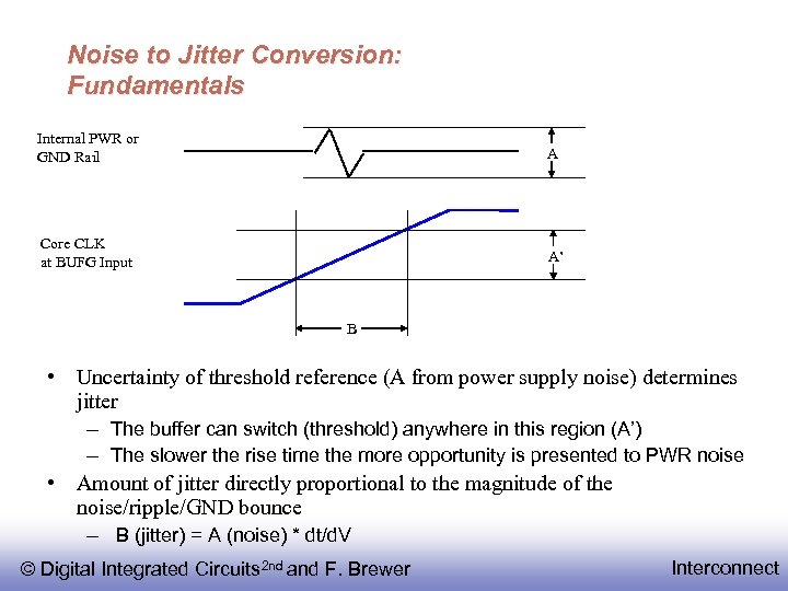 Noise to Jitter Conversion: Fundamentals Internal PWR or GND Rail A Core CLK at BUFG Input A’ B • Uncertainty of threshold reference (A from power supply noise) determines jitter – The buffer can switch (threshold) anywhere in this region (A’) – The slower the rise time the more opportunity is presented to PWR noise • Amount of jitter directly proportional to the magnitude of the noise/ripple/GND bounce – B (jitter) = A (noise) * dt/d. V © Digital Integrated Circuits 2 nd and F. Brewer Interconnect
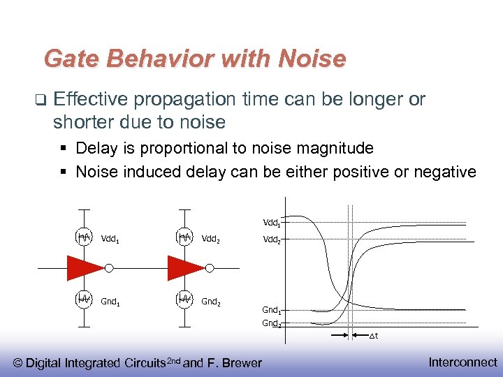 Gate Behavior with Noise Effective propagation time can be longer or shorter due to noise § Delay is proportional to noise magnitude § Noise induced delay can be either positive or negative Vdd 1 Vdd 2 Gnd 1 Gnd 2 t © Digital Integrated Circuits 2 nd and F. Brewer Interconnect
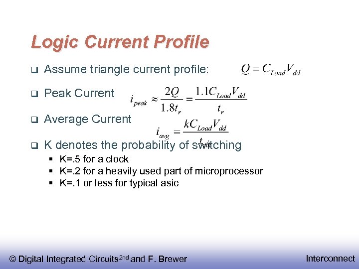 Logic Current Profile Assume triangle current profile: Peak Current Average Current K denotes the probability of switching § K=. 5 for a clock § K=. 2 for a heavily used part of microprocessor § K=. 1 or less for typical asic © Digital Integrated Circuits 2 nd and F. Brewer Interconnect
 Power Distribution Low-level distribution is in Metal 1 § Higher Resistance Power has to be ‘strapped’ in higher layers of metal. The spacing is set by IR drop, electromigration, inductive effects Always use multiple contacts on straps © Digital Integrated Circuits 2 nd and F. Brewer Interconnect
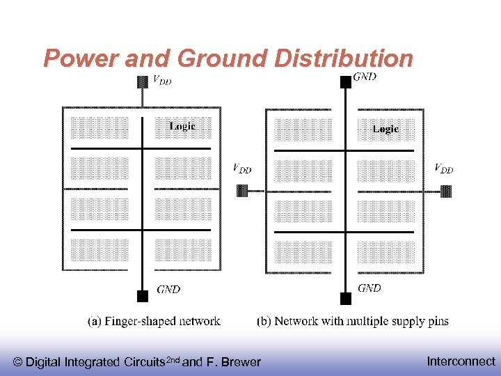 Power and Ground Distribution © Digital Integrated Circuits 2 nd and F. Brewer Interconnect
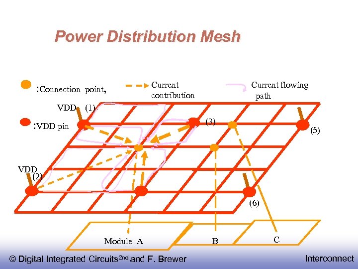 Power Distribution Mesh : Connection point, Current contribution Current flowing path VDD (1) (3) : VDD pin (5) VDD (2) (6) Module A © Digital Integrated Circuits 2 nd and F. Brewer B C Interconnect
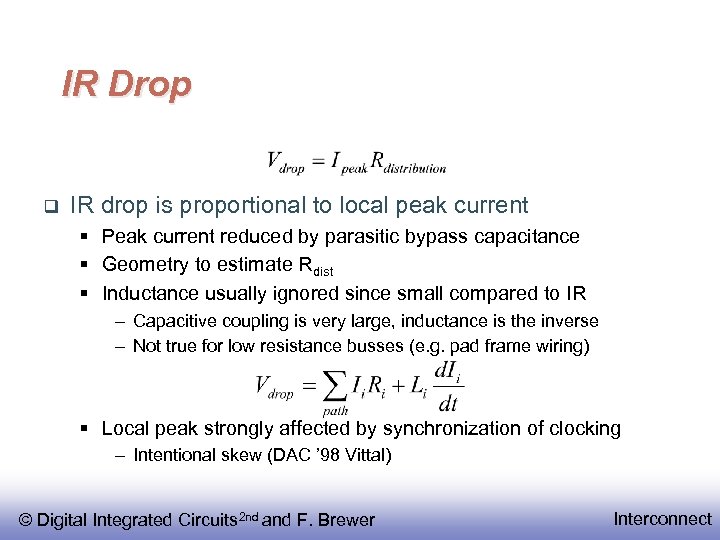 IR Drop IR drop is proportional to local peak current § Peak current reduced by parasitic bypass capacitance § Geometry to estimate Rdist § Inductance usually ignored since small compared to IR – Capacitive coupling is very large, inductance is the inverse – Not true for low resistance busses (e. g. pad frame wiring) § Local peak strongly affected by synchronization of clocking – Intentional skew (DAC ’ 98 Vittal) © Digital Integrated Circuits 2 nd and F. Brewer Interconnect
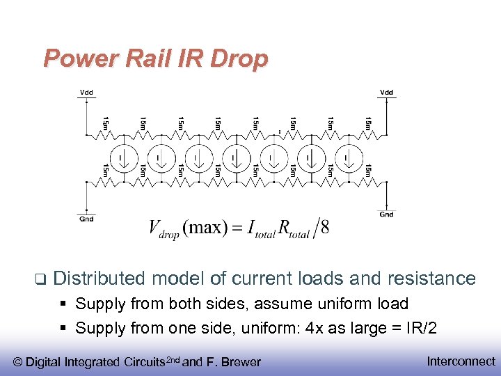 Power Rail IR Drop Distributed model of current loads and resistance § Supply from both sides, assume uniform load § Supply from one side, uniform: 4 x as large = IR/2 © Digital Integrated Circuits 2 nd and F. Brewer Interconnect
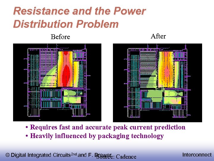 Resistance and the Power Distribution Problem Before After • Requires fast and accurate peak current prediction • Heavily influenced by packaging technology © Digital Integrated Circuits 2 nd and F. Brewer Cadence Source: Interconnect
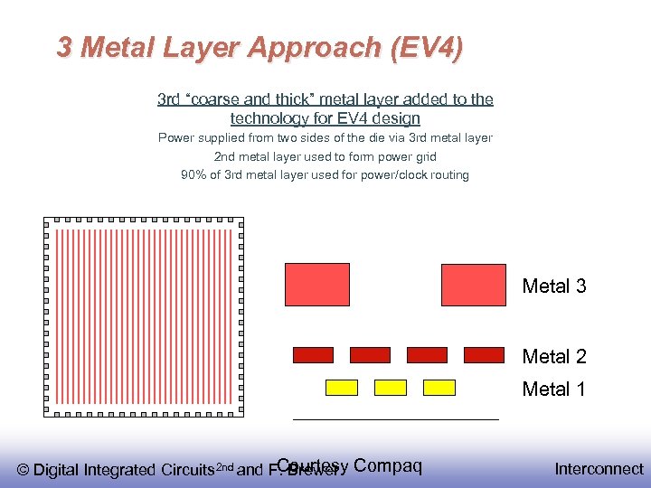 3 Metal Layer Approach (EV 4) 3 rd “coarse and thick” metal layer added to the technology for EV 4 design Power supplied from two sides of the die via 3 rd metal layer 2 nd metal layer used to form power grid 90% of 3 rd metal layer used for power/clock routing Metal 3 Metal 2 Metal 1 Courtesy © Digital Integrated Circuits 2 nd and F. Brewer Compaq Interconnect
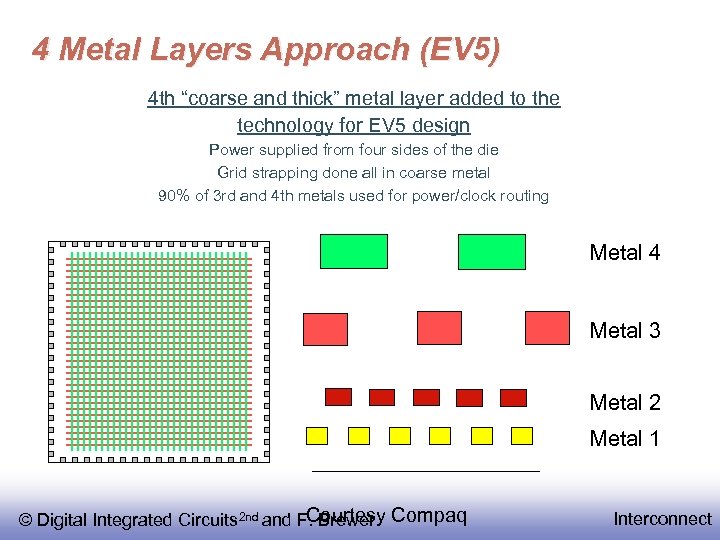 4 Metal Layers Approach (EV 5) 4 th “coarse and thick” metal layer added to the technology for EV 5 design Power supplied from four sides of the die Grid strapping done all in coarse metal 90% of 3 rd and 4 th metals used for power/clock routing Metal 4 Metal 3 Metal 2 Metal 1 Courtesy © Digital Integrated Circuits 2 nd and F. Brewer Compaq Interconnect
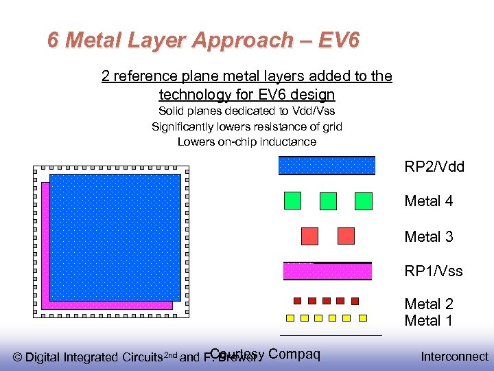 6 Metal Layer Approach – EV 6 2 reference plane metal layers added to the technology for EV 6 design Solid planes dedicated to Vdd/Vss Significantly lowers resistance of grid Lowers on-chip inductance RP 2/Vdd Metal 4 Metal 3 RP 1/Vss Metal 2 Metal 1 Courtesy © Digital Integrated Circuits 2 nd and F. Brewer Compaq Interconnect
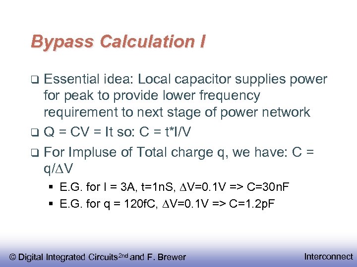 Bypass Calculation I Essential idea: Local capacitor supplies power for peak to provide lower frequency requirement to next stage of power network Q = CV = It so: C = t*I/V For Impluse of Total charge q, we have: C = q/ V § E. G. for I = 3 A, t=1 n. S, V=0. 1 V => C=30 n. F § E. G. for q = 120 f. C, V=0. 1 V => C=1. 2 p. F © Digital Integrated Circuits 2 nd and F. Brewer Interconnect
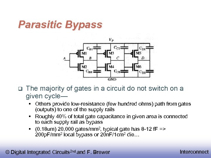 Parasitic Bypass The majority of gates in a circuit do not switch on a given cycle— § Others provide low-resistance (few hundred ohms) path from gates (outputs) to one of the supply rails § Roughly 40% of total gate capacitance in given area is connected to each supply rail as bypass § (0. 18 um) 20, 000 gates/mm 2, typical gate has 8 -12 f. F => 200 p. F/mm 2 local bypass or 20 n. F/1 cm 2 die… © Digital Integrated Circuits 2 nd and F. Brewer Interconnect
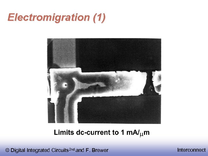 Electromigration (1) © Digital Integrated Circuits 2 nd and F. Brewer Interconnect
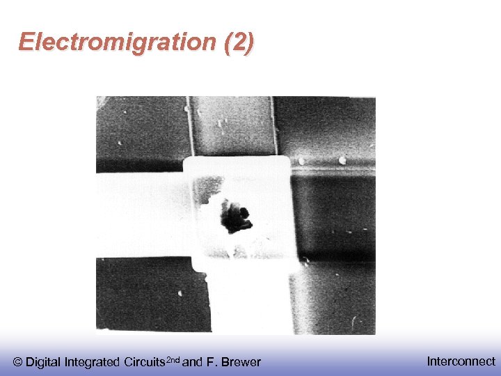 Electromigration (2) © Digital Integrated Circuits 2 nd and F. Brewer Interconnect
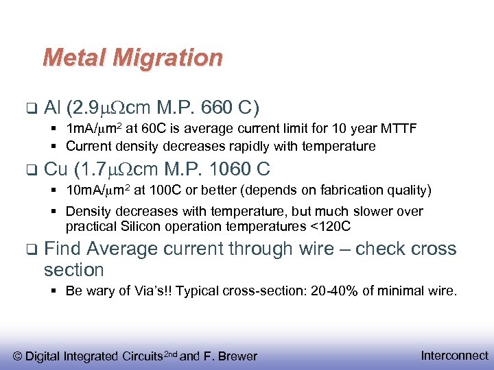 Metal Migration Al (2. 9 Wcm M. P. 660 C) § 1 m. A/ m 2 at 60 C is average current limit for 10 year MTTF § Current density decreases rapidly with temperature Cu (1. 7 Wcm M. P. 1060 C § 10 m. A/ m 2 at 100 C or better (depends on fabrication quality) § Density decreases with temperature, but much slower over practical Silicon operation temperatures <120 C Find Average current through wire – check cross section § Be wary of Via’s!! Typical cross-section: 20 -40% of minimal wire. © Digital Integrated Circuits 2 nd and F. Brewer Interconnect
 Clocking © Digital Integrated Circuits 2 nd and F. Brewer Interconnect
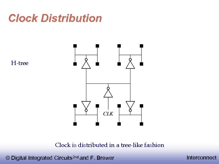 Clock Distribution H-tree Clock is distributed in a tree-like fashion © Digital Integrated Circuits 2 nd and F. Brewer Interconnect
![More realistic H-tree [Restle 98] © Digital Integrated Circuits 2 nd and F. Brewer More realistic H-tree [Restle 98] © Digital Integrated Circuits 2 nd and F. Brewer](https://present5.com/presentation/fd9d596579e5623f1a808c51bd82e18d/image-24.jpg) More realistic H-tree [Restle 98] © Digital Integrated Circuits 2 nd and F. Brewer Interconnect
More realistic H-tree [Restle 98] © Digital Integrated Circuits 2 nd and F. Brewer Interconnect
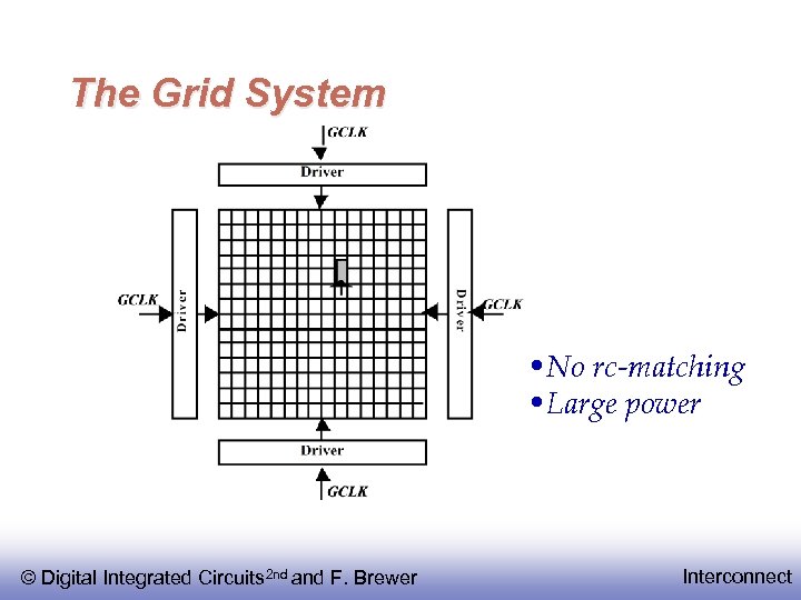 The Grid System • No rc-matching • Large power © Digital Integrated Circuits 2 nd and F. Brewer Interconnect
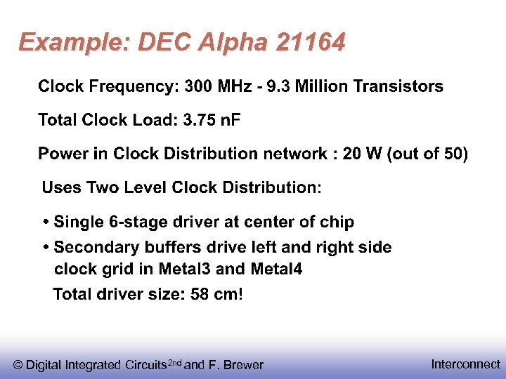 Example: DEC Alpha 21164 © Digital Integrated Circuits 2 nd and F. Brewer Interconnect
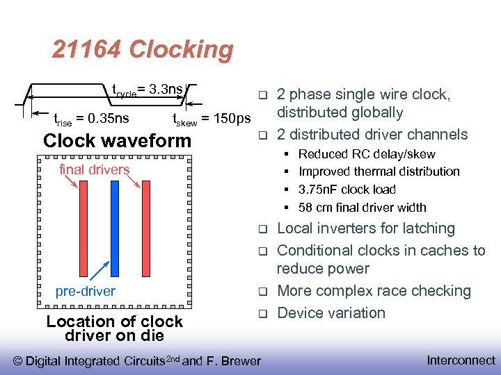 21164 Clocking tcycle= 3. 3 ns trise = 0. 35 ns tskew = 150 ps Clock waveform § § final drivers pre-driver Location of clock driver on die 2 phase single wire clock, distributed globally 2 distributed driver channels © Digital Integrated Circuits 2 nd and F. Brewer Reduced RC delay/skew Improved thermal distribution 3. 75 n. F clock load 58 cm final driver width Local inverters for latching Conditional clocks in caches to reduce power More complex race checking Device variation Interconnect
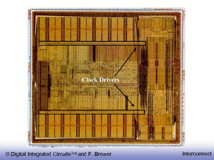 © Digital Integrated Circuits 2 nd and F. Brewer Interconnect
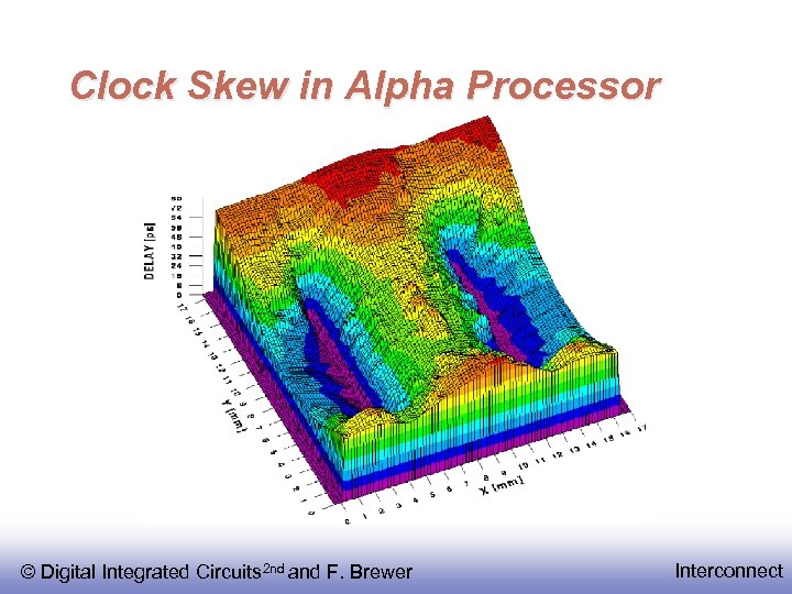 Clock Skew in Alpha Processor © Digital Integrated Circuits 2 nd and F. Brewer Interconnect
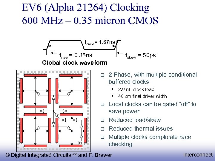 EV 6 (Alpha 21264) Clocking 600 MHz – 0. 35 micron CMOS tcycle= 1. 67 ns trise = 0. 35 ns Global clock waveform tskew = 50 ps 2 Phase, with multiple conditional buffered clocks § 2. 8 n. F clock load § 40 cm final driver width Local clocks can be gated “off” to save power Reduced load/skew Reduced thermal issues Multiple clocks complicate race checking © Digital Integrated Circuits 2 nd and F. Brewer Interconnect
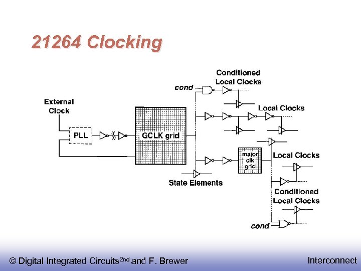 21264 Clocking © Digital Integrated Circuits 2 nd and F. Brewer Interconnect
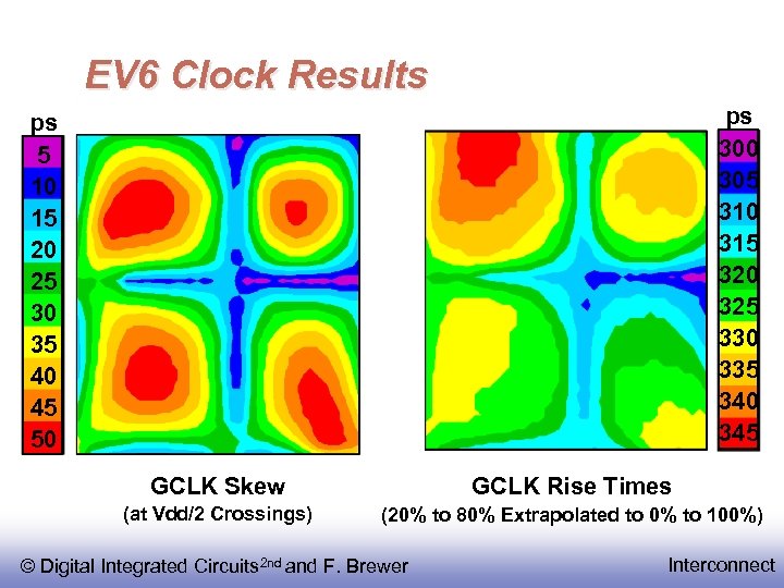 EV 6 Clock Results ps 300 305 310 315 320 325 330 335 340 345 ps 5 10 15 20 25 30 35 40 45 50 GCLK Skew GCLK Rise Times (at Vdd/2 Crossings) (20% to 80% Extrapolated to 0% to 100%) © Digital Integrated Circuits 2 nd and F. Brewer Interconnect
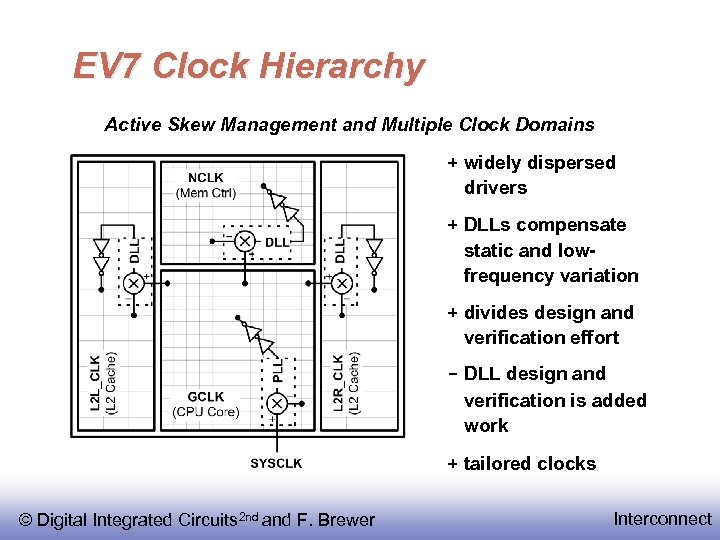 EV 7 Clock Hierarchy Active Skew Management and Multiple Clock Domains + widely dispersed drivers + DLLs compensate static and lowfrequency variation + divides design and verification effort - DLL design and verification is added work + tailored clocks © Digital Integrated Circuits 2 nd and F. Brewer Interconnect
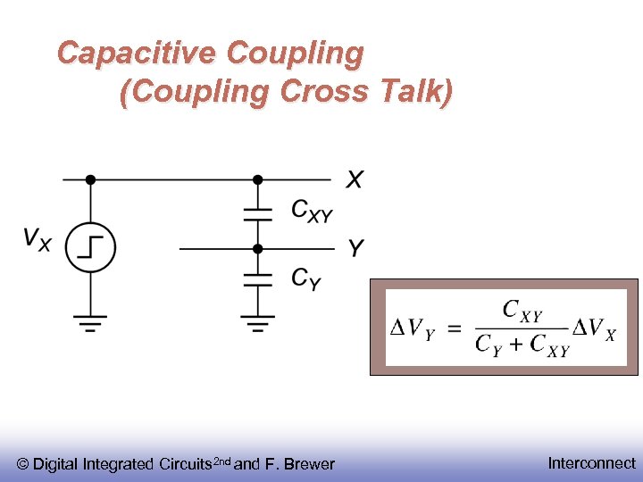 Capacitive Coupling (Coupling Cross Talk) © Digital Integrated Circuits 2 nd and F. Brewer Interconnect
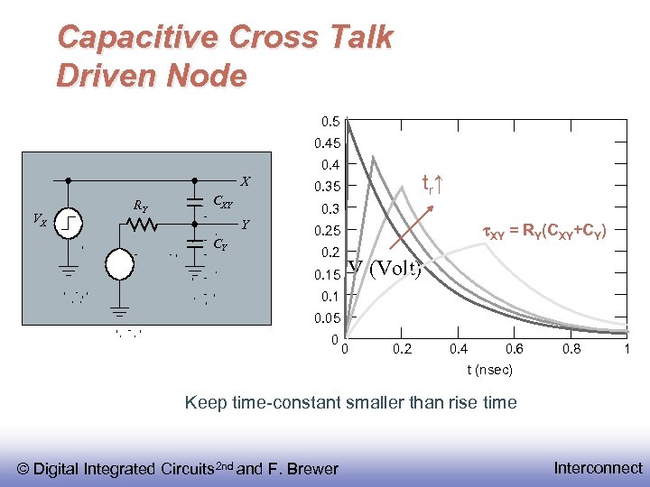 Capacitive Cross Talk Driven Node 0. 5 0. 4 X VX RY CXY 0. 3 Y CY t r↑ 0. 35 t. XY = RY(CXY+CY) 0. 25 0. 2 0. 15 V (Volt) 0. 1 0. 05 0 0 0. 2 0. 4 0. 6 0. 8 1 t (nsec) Keep time-constant smaller than rise time © Digital Integrated Circuits 2 nd and F. Brewer Interconnect
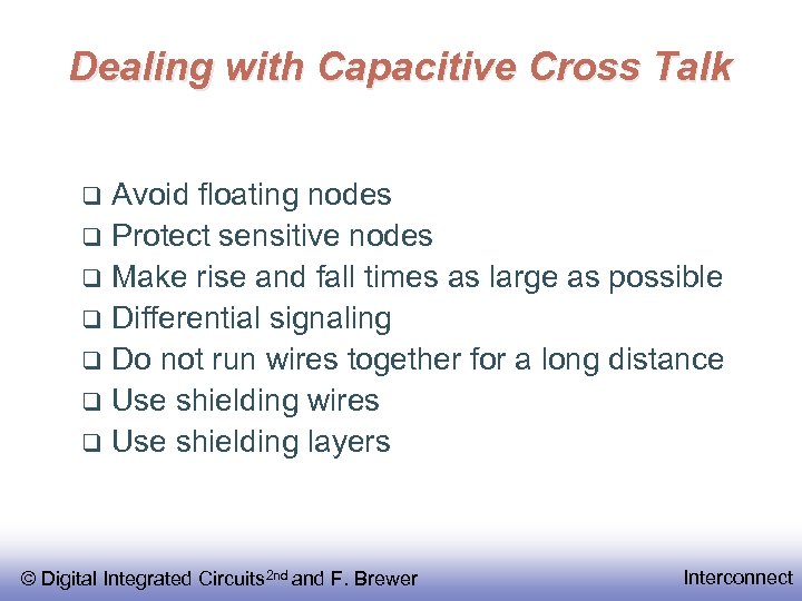 Dealing with Capacitive Cross Talk Avoid floating nodes Protect sensitive nodes Make rise and fall times as large as possible Differential signaling Do not run wires together for a long distance Use shielding wires Use shielding layers © Digital Integrated Circuits 2 nd and F. Brewer Interconnect
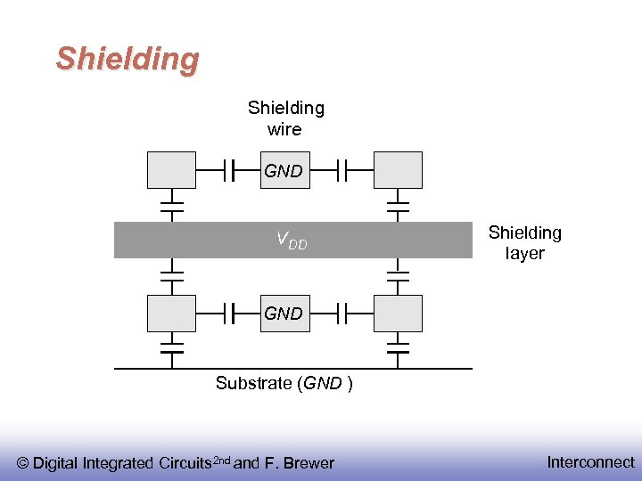 Shielding wire GND V DD Shielding layer GND Substrate (GND ) © Digital Integrated Circuits 2 nd and F. Brewer Interconnect
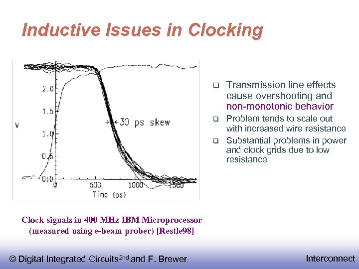 Inductive Issues in Clocking Transmission line effects cause overshooting and non-monotonic behavior Problem tends to scale out with increased wire resistance Substantial problems in power and clock grids due to low resistance Clock signals in 400 MHz IBM Microprocessor (measured using e-beam prober) [Restle 98] © Digital Integrated Circuits 2 nd and F. Brewer Interconnect
 Packaging and Board Interface © Digital Integrated Circuits 2 nd and F. Brewer Interconnect
 Packaging Requirements Electrical: Low parasitics Mechanical: Reliable and robust Thermal: Efficient heat removal Economical: Cheap © Digital Integrated Circuits 2 nd and F. Brewer Interconnect
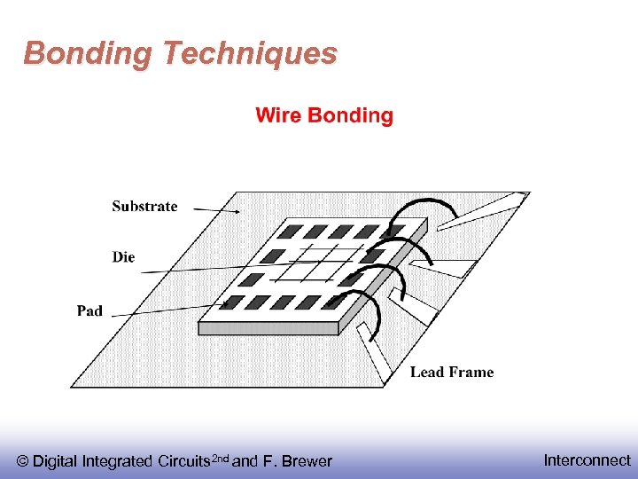 Bonding Techniques © Digital Integrated Circuits 2 nd and F. Brewer Interconnect
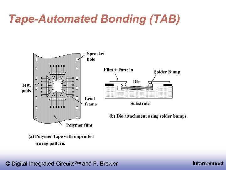 Tape-Automated Bonding (TAB) © Digital Integrated Circuits 2 nd and F. Brewer Interconnect
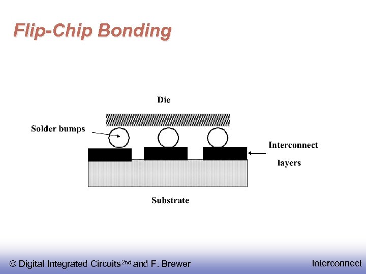 Flip-Chip Bonding © Digital Integrated Circuits 2 nd and F. Brewer Interconnect
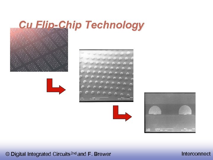 Cu Flip-Chip Technology © Digital Integrated Circuits 2 nd and F. Brewer Interconnect
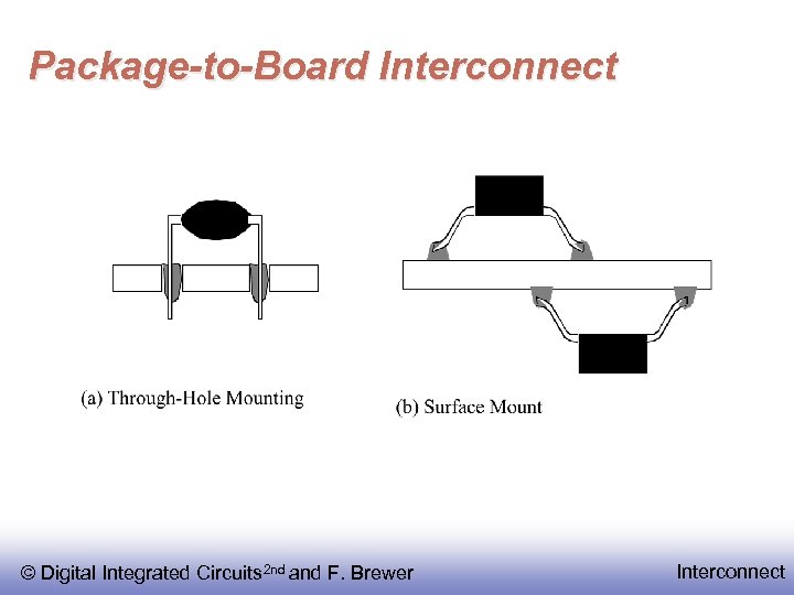 Package-to-Board Interconnect © Digital Integrated Circuits 2 nd and F. Brewer Interconnect
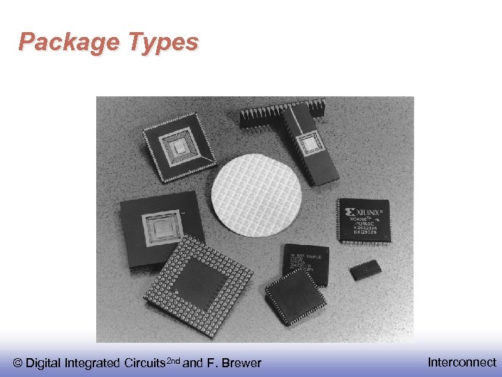 Package Types © Digital Integrated Circuits 2 nd and F. Brewer Interconnect
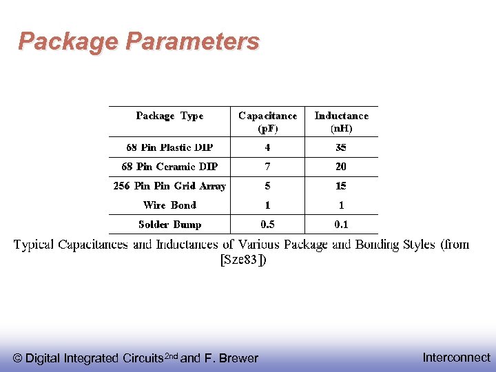 Package Parameters © Digital Integrated Circuits 2 nd and F. Brewer Interconnect
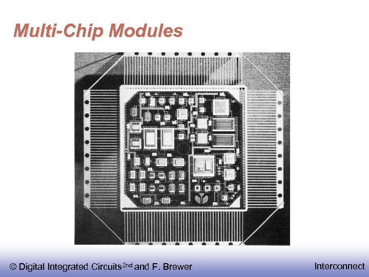 Multi-Chip Modules © Digital Integrated Circuits 2 nd and F. Brewer Interconnect
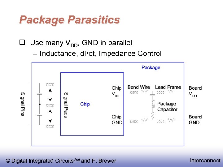 Package Parasitics Use many VDD, GND in parallel – Inductance, d. I/dt, Impedance Control © Digital Integrated Circuits 2 nd and F. Brewer Interconnect
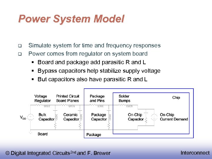 Power System Model Simulate system for time and frequency responses Power comes from regulator on system board § Board and package add parasitic R and L § Bypass capacitors help stabilize supply voltage § But capacitors also have parasitic R and L © Digital Integrated Circuits 2 nd and F. Brewer Interconnect
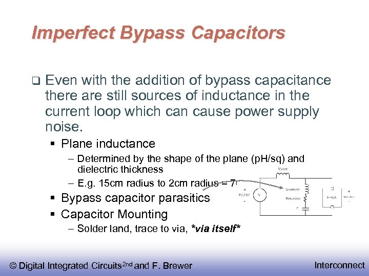 Imperfect Bypass Capacitors Even with the addition of bypass capacitance there are still sources of inductance in the current loop which can cause power supply noise. § Plane inductance – Determined by the shape of the plane (p. H/sq) and dielectric thickness – E. g. 15 cm radius to 2 cm radius = 70 p. H § Bypass capacitor parasitics § Capacitor Mounting – Solder land, trace to via, *via itself* © Digital Integrated Circuits 2 nd and F. Brewer Interconnect
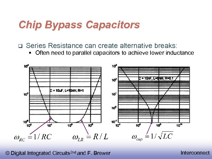 Chip Bypass Capacitors Series Resistance can create alternative breaks: § Often need to parallel capacitors to achieve lower inductance © Digital Integrated Circuits 2 nd and F. Brewer Interconnect
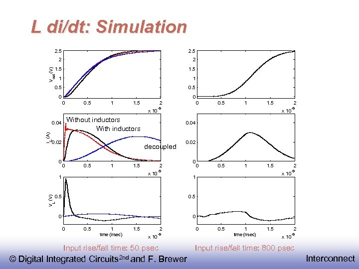
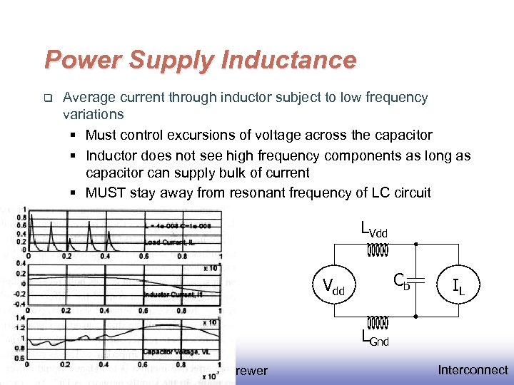 Power Supply Inductance Average current through inductor subject to low frequency variations § Must control excursions of voltage across the capacitor § Inductor does not see high frequency components as long as capacitor can supply bulk of current § MUST stay away from resonant frequency of LC circuit LVdd Cb Vdd IL LGnd © Digital Integrated Circuits 2 nd and F. Brewer Interconnect
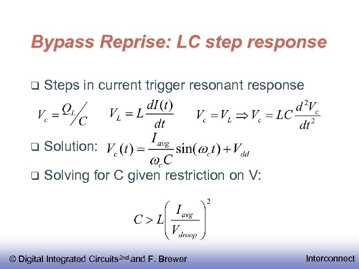 Bypass Reprise: LC step response Steps in current trigger resonant response Solution: Solving for C given restriction on V: © Digital Integrated Circuits 2 nd and F. Brewer Interconnect
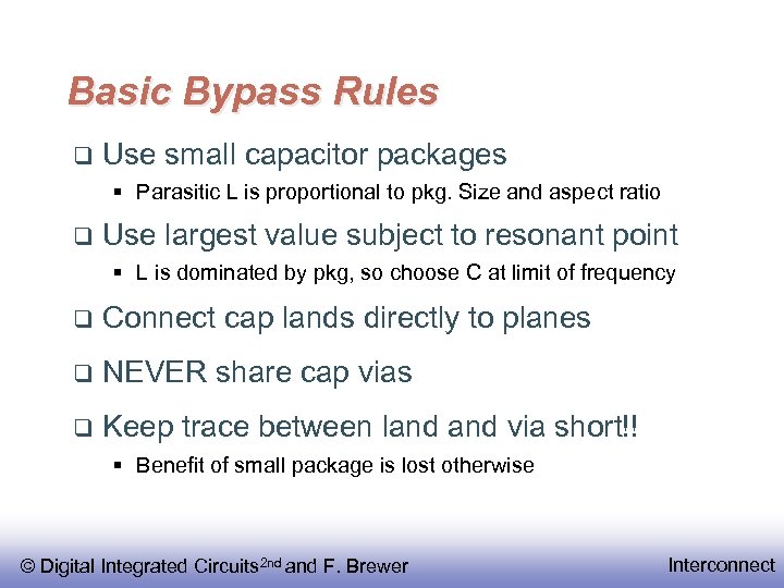 Basic Bypass Rules Use small capacitor packages § Parasitic L is proportional to pkg. Size and aspect ratio Use largest value subject to resonant point § L is dominated by pkg, so choose C at limit of frequency Connect cap lands directly to planes NEVER share cap vias Keep trace between land via short!! § Benefit of small package is lost otherwise © Digital Integrated Circuits 2 nd and F. Brewer Interconnect
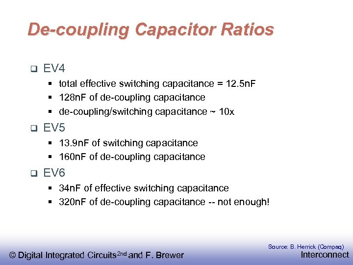 De-coupling Capacitor Ratios EV 4 § total effective switching capacitance = 12. 5 n. F § 128 n. F of de-coupling capacitance § de-coupling/switching capacitance ~ 10 x EV 5 § 13. 9 n. F of switching capacitance § 160 n. F of de-coupling capacitance EV 6 § 34 n. F of effective switching capacitance § 320 n. F of de-coupling capacitance -- not enough! Source: B. Herrick (Compaq) © Digital Integrated Circuits 2 nd and F. Brewer Interconnect
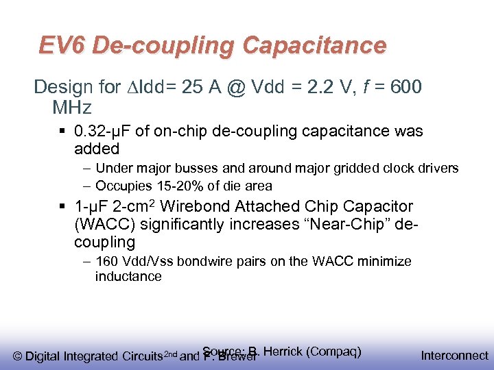 EV 6 De-coupling Capacitance Design for Idd= 25 A @ Vdd = 2. 2 V, f = 600 MHz § 0. 32 -µF of on-chip de-coupling capacitance was added – Under major busses and around major gridded clock drivers – Occupies 15 -20% of die area § 1 -µF 2 -cm 2 Wirebond Attached Chip Capacitor (WACC) significantly increases “Near-Chip” decoupling – 160 Vdd/Vss bondwire pairs on the WACC minimize inductance © Digital Integrated Circuits 2 nd and Source: B. Herrick (Compaq) F. Brewer Interconnect
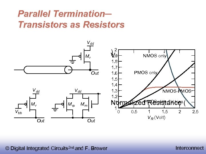
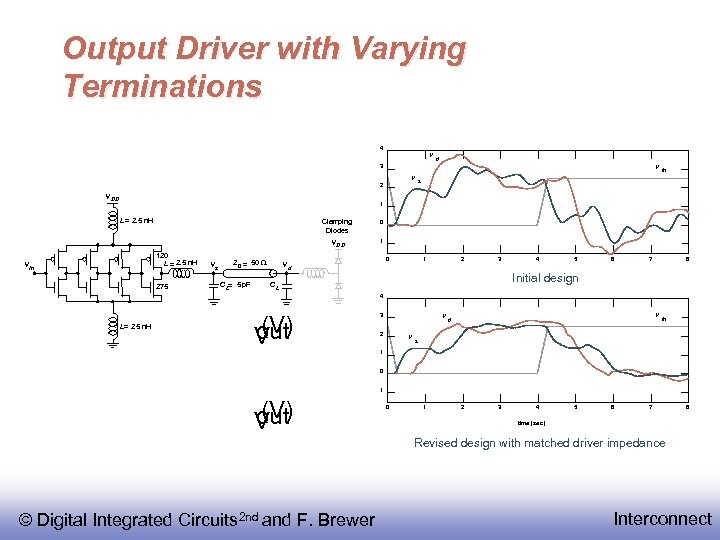
 PCB Signaling Circuit traces on PCB are transmission lines § Impedance Matching § Resistor model during drive § Pad Rise/Fall times are independent of far-end load in many cases § Scale: 6 -8 in/n. S © Digital Integrated Circuits 2 nd and F. Brewer Interconnect
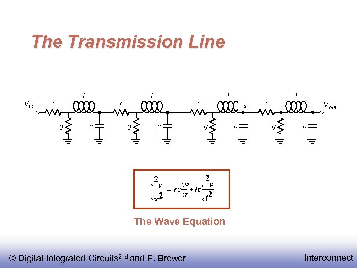 The Transmission Line V in l r g l r c x g c l r V out g c The Wave Equation © Digital Integrated Circuits 2 nd and F. Brewer Interconnect
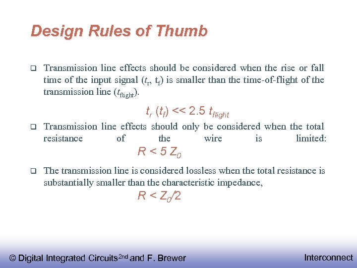 Design Rules of Thumb Transmission line effects should be considered when the rise or fall time of the input signal (tr, tf) is smaller than the time-of-flight of the transmission line (tflight). tr (tf) << 2. 5 tflight Transmission line effects should only be considered when the total resistance of the wire is limited: R < 5 Z 0 The transmission line is considered lossless when the total resistance is substantially smaller than the characteristic impedance, R < Z 0/2 © Digital Integrated Circuits 2 nd and F. Brewer Interconnect
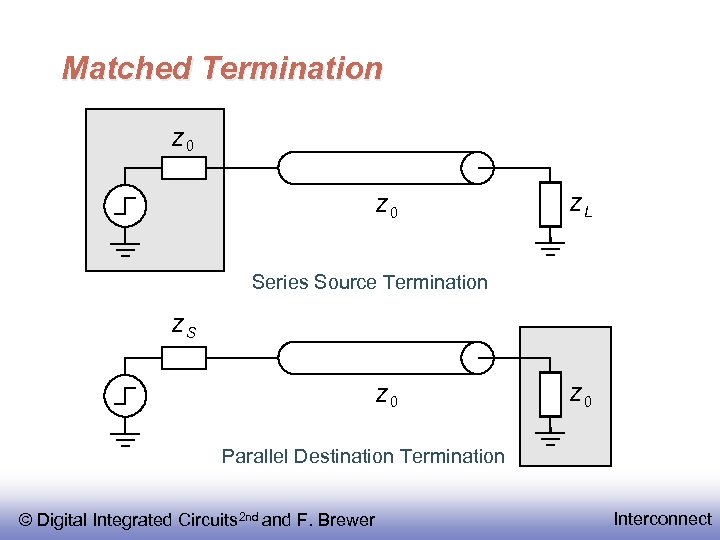 Matched Termination Z 0 ZL Series Source Termination ZS Z 0 Parallel Destination Termination © Digital Integrated Circuits 2 nd and F. Brewer Interconnect
 Parallel Termination─ Transistors as Resistors V dd )2 1. 9 V Mr Out Vdd Mr Vdd M rp M rn V bb Out © Digital Integrated Circuits 2 nd and F. Brewer NMOS only 1. 8 1. 7 PMOS only 1. 6 1. 5 1. 4 1. 3 NMOS-PMOS 1. 2 PMOS with-1 V bias 1. 1 Normalized Resistance ( 1 0 0. 5 1 1. 5 2 2. 5 VR (Volt) Interconnect
 Output Driver with Varying Terminations 4 V d 3 V V 2 V DD in s 1 L = 2. 5 n. H Clamping Diodes V DD 120 L = 2. 5 n. H V in 275 Vs Z 0 = 50 W C L= 5 p. F 0 1 0 Vd 1 2 3 4 5 6 7 8 Initial design CL 4 L= 2. 5 n. H (V) o Vut 3 V 2 V V d in s 1 0 1 (V) o Vut 0 1 2 3 4 5 6 7 8 time (sec) Revised design with matched driver impedance © Digital Integrated Circuits 2 nd and F. Brewer Interconnect
 L di/dt V DD L i(t) V ’DD V out V in CL GND ’ L Impact of inductance on supply voltages: • Change in current induces a change in voltage • Longer supply lines have larger L • Note: idealized model for decoupling Capacitor! • Given model is ok for on-chip • Ignores off-chip package inductances of both chip and capacitor • Decoupling solutions need to cover all time scales of switching • Board-level (to 10’s of MHz) • Package-level (200 MHz) • On-Chip (above 200 MHz) © Digital Integrated Circuits 2 nd and F. Brewer Interconnect
 L di/dt: Simulation 2 1. 5 out 2. 5 2 (V) 2. 5 1 0. 5 V 1 0 0. 5 1 1. 5 2 x 10 Without inductors With inductors 0. 02 0 decoupled 0 0. 5 1 1. 5 2 -9 x 10 -9 0. 02 0 0 0. 5 1 1. 5 -9 1 0. 5 2 0. 5 L V (V) 1 x 10 2 x 10 1 0. 5 0. 04 L i (A) 0. 04 0 -9 0 0. 5 1 time (nsec) 1. 5 2 x 10 -9 Input rise/fall time: 50 psec © Digital Integrated Circuits 2 nd and F. Brewer 0 0. 5 1 time (nsec) 1. 5 2 Input rise/fall time: 800 psec Interconnect
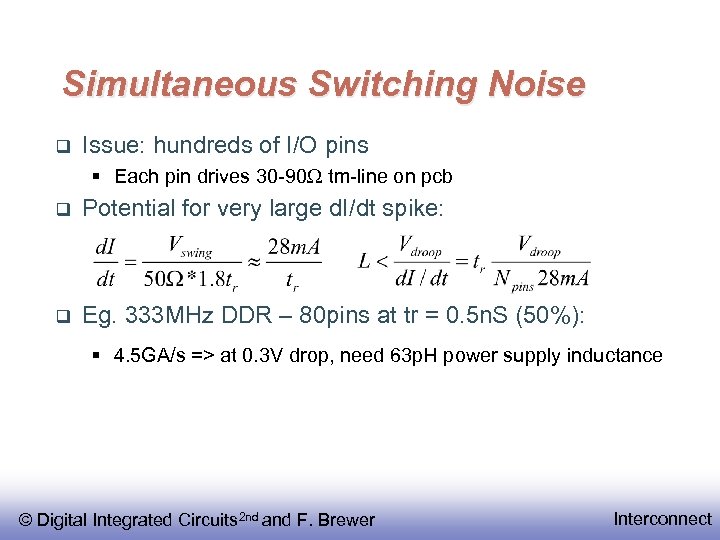 Simultaneous Switching Noise Issue: hundreds of I/O pins § Each pin drives 30 -90 W tm-line on pcb Potential for very large d. I/dt spike: Eg. 333 MHz DDR – 80 pins at tr = 0. 5 n. S (50%): § 4. 5 GA/s => at 0. 3 V drop, need 63 p. H power supply inductance © Digital Integrated Circuits 2 nd and F. Brewer Interconnect
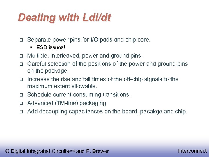 Dealing with Ldi/dt Separate power pins for I/O pads and chip core. § ESD issues! Multiple, interleaved, power and ground pins. Careful selection of the positions of the power and ground pins on the package. Increase the rise and fall times of the off-chip signals to the maximum extent allowable. Schedule current-consuming transitions. Advanced (TM-line) packaging Add decoupling capacitances on the board, pacakge and chip. © Digital Integrated Circuits 2 nd and F. Brewer Interconnect
 EV 6 WACC © Digital Integrated Circuits 2 nd and. Source: B. Herrick (Compaq) F. Brewer Interconnect
 Pads © Digital Integrated Circuits 2 nd and F. Brewer Interconnect
 Pads-- Chip to Board Interface Pads drive large Capacitances § 5 pf minimum to much larger § Rise time control Board Impeadance and Noise § L d. I/dt Noise Coupling to Power Distribution ESD © Digital Integrated Circuits 2 nd and F. Brewer Interconnect
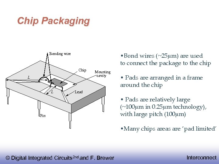 Chip Packaging Bonding wire • Bond wires (~25 m) are used to connect the package to the chip Chip L L Mounting cavity • Pads are arranged in a frame around the chip Lead Pin • Pads are relatively large (~100 m in 0. 25 m technology), with large pitch (100 m) • Many chips areas are ‘pad limited’ © Digital Integrated Circuits 2 nd and F. Brewer Interconnect
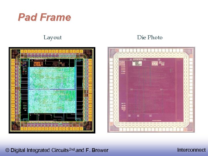 Pad Frame Layout © Digital Integrated Circuits 2 nd and F. Brewer Die Photo Interconnect
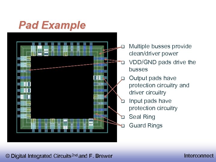 Pad Example © Digital Integrated Circuits 2 nd and F. Brewer Multiple busses provide clean/driver power VDD/GND pads drive the busses Output pads have protection circuitry and driver circuitry Input pads have protection circuitry Seal Ring Guard Rings Interconnect
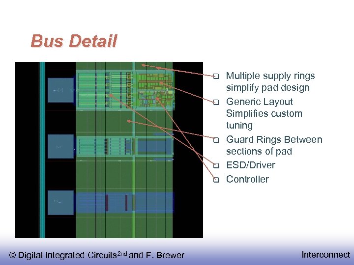 Bus Detail © Digital Integrated Circuits 2 nd and F. Brewer Multiple supply rings simplify pad design Generic Layout Simplifies custom tuning Guard Rings Between sections of pad ESD/Driver Controller Interconnect
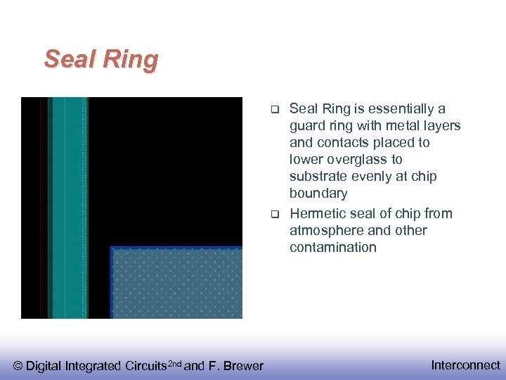 Seal Ring © Digital Integrated Circuits 2 nd and F. Brewer Seal Ring is essentially a guard ring with metal layers and contacts placed to lower overglass to substrate evenly at chip boundary Hermetic seal of chip from atmosphere and other contamination Interconnect
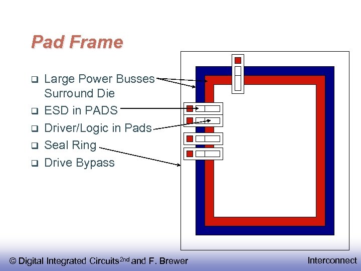 Pad Frame Large Power Busses Surround Die ESD in PADS Driver/Logic in Pads Seal Ring Drive Bypass © Digital Integrated Circuits 2 nd and F. Brewer Interconnect
 Chip to Board Interface -- Pad Design Buffer to drive PCB-scale parasitics § Capacitance 5 -50 p. F, Impedance 30 -90 W Rise-Time Control § Noise injection to circuits and power supply ESD § Protection of chip-scale components Perimeter Pads/Area Bump © Digital Integrated Circuits 2 nd and F. Brewer Interconnect
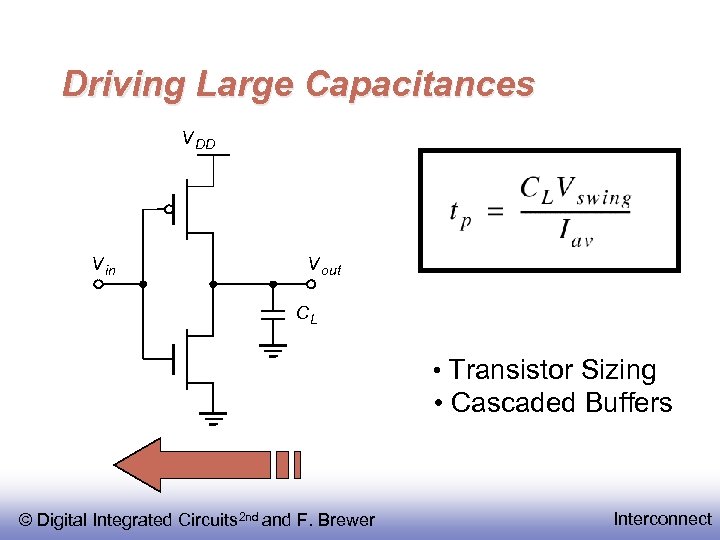 Driving Large Capacitances V DD V in V out CL • Transistor Sizing • Cascaded Buffers © Digital Integrated Circuits 2 nd and F. Brewer Interconnect
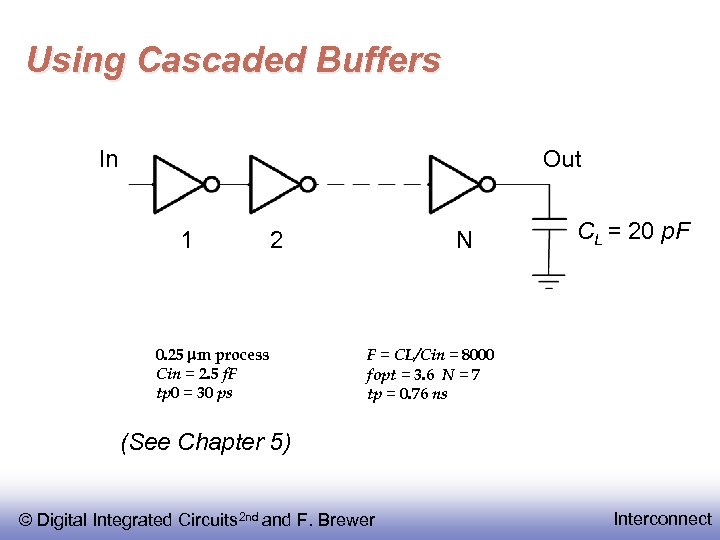 Using Cascaded Buffers In Out 1 2 0. 25 mm process Cin = 2. 5 f. F tp 0 = 30 ps N CL = 20 p. F F = CL/Cin = 8000 fopt = 3. 6 N = 7 tp = 0. 76 ns (See Chapter 5) © Digital Integrated Circuits 2 nd and F. Brewer Interconnect
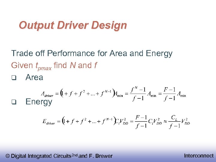 Output Driver Design Trade off Performance for Area and Energy Given tpmax find N and f Area Energy © Digital Integrated Circuits 2 nd and F. Brewer Interconnect
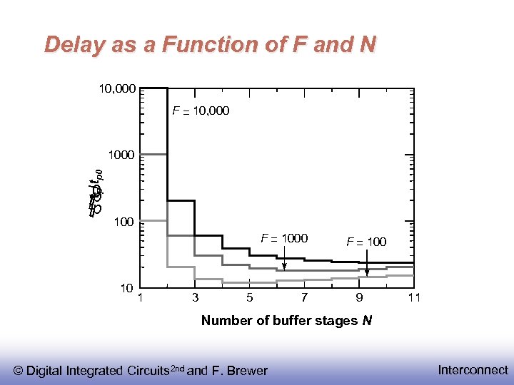 Delay as a Function of F and N 10, 000 F = 10, 000 tp/tp 0 1000 t 0 /p tp 100 F = 1000 10 1 3 5 7 F = 100 9 11 Number of buffer stages N © Digital Integrated Circuits 2 nd and F. Brewer Interconnect
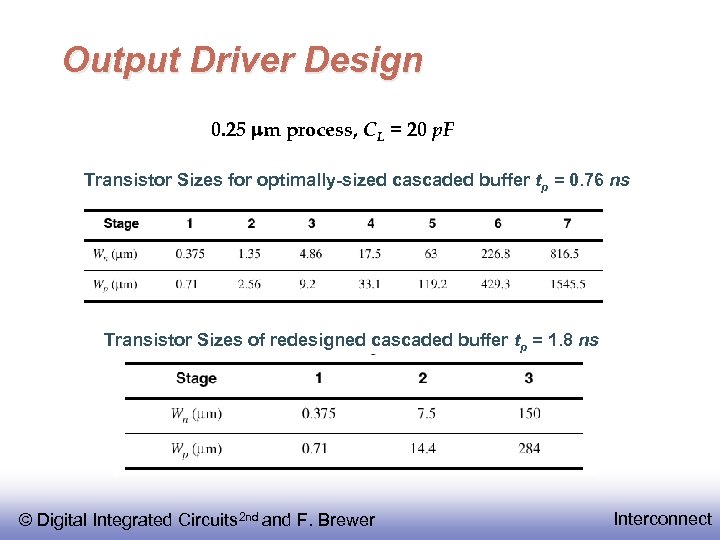 Output Driver Design 0. 25 mm process, CL = 20 p. F Transistor Sizes for optimally-sized cascaded buffer tp = 0. 76 ns Transistor Sizes of redesigned cascaded buffer tp = 1. 8 ns © Digital Integrated Circuits 2 nd and F. Brewer Interconnect
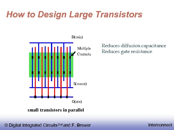 How to Design Large Transistors D(rain) Multiple Contacts Reduces diffusion capacitance Reduces gate resistance S(ource) G(ate) small transistors in parallel © Digital Integrated Circuits 2 nd and F. Brewer Interconnect
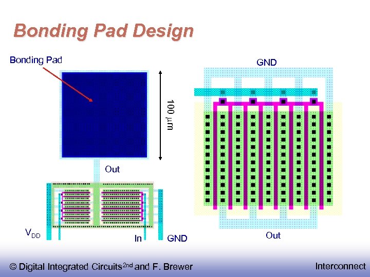 Bonding Pad Design Bonding Pad GND 100 m Out VDD In GND © Digital Integrated Circuits 2 nd and F. Brewer Out Interconnect
 ESD Protection When a chip is connected to a board, there is unknown (potentially large) static voltage difference Equalizing potentials requires (large) charge flow through the pads Diodes sink this charge into the substrate – need guard rings to pick it up. © Digital Integrated Circuits 2 nd and F. Brewer Interconnect
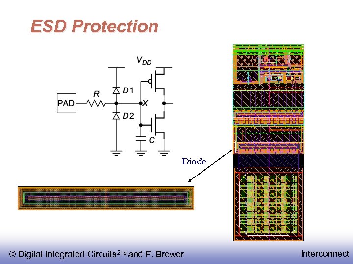 ESD Protection Diode © Digital Integrated Circuits 2 nd and F. Brewer Interconnect


