fpga_presentation.ppt
- Количество слайдов: 43
 Проектирование систем на ПЛИС
 Рисунок 1 – Внутренняя структура ПЛИС
 Рисунок 2 – Логический блок на мультиплексорах
 Рисунок 3 – Требуемая функция и соответствующая ей таблица истинности
 Рисунок 4 – Таблица соответствия на основе передаточных вентилей
 Рисунок 6 – Многофункциональная таблица соответствия Рисунок 5 – Конфигурационные ячейки, связанные в цепочку
 Рисунок 7 – Упрощенный вид логической ячейки Xilinx
 Рисунок 8 – Секция, содержащая две логических ячейки
 Рисунок 9 – Конфигурируемый логический блок, содержащий четыре секции
 Рисунок 10 – Вид на кристалл со столбцами встроенных блоков ОЗУ
 Рисунок 11 – Вид на кристалл со столбцами встроенных умножителей и блоков ОЗУ
 Рисунок 12 – Функции, формирующие операцию умножения с накоплением
 Рисунок 13 – Вид на кристалл со встроенным ядром, находящимся за пределами главной части
 Рисунок 14 – Вид на кристаллы с ядрами, встроенными внутрь главной части
 Основы языка Verilog HDL
 Тип источника сигнала wire 1 wire a; 2 3 wire b; assign a = b; 4 wire a = b; 5 wire [3: 0] c; //это четыре провода 6 7 wire [3: 0] d; assign c = d; //“подключение” одной шины к другой 8 9 wire [11: 4] e; //восьмибитная шина wire [0: 255] f; //256 -ти битная шина 10 11 wire g; assign g = f[2]; //назначить сигналу “g” второй бит шины “f” 12 13 wire [7: 0] h; wire i = f[h]; // назначить сигналу “i” бит номер “h” из шины “f”
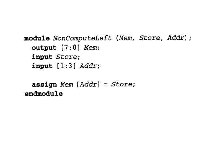
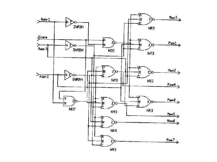
![14 wire [3: 0] j = e[7: 4]; 15 wire [7: 0] k [0:](https://present5.com/presentation/3/26829759_438461642.pdf-img/26829759_438461642.pdf-17.jpg "14 wire [3: 0] j = e[7: 4]; 15 wire [7: 0] k [0:") 14 wire [3: 0] j = e[7: 4]; 15 wire [7: 0] k [0: 19]; //массив из двадцати 8 -ми битных шин Тип источника сигнала reg 16 17 reg [3: 0] m; reg [0: 100] n; 18 wire [1: 0] p = m[2: 1]; 19 reg [7: 0] q [0: 15]; //память из 16 слов, каждое по 8 бит 20 integer loop_count; 21 22 23 24 25 Модули (module) module my_module_name (port_a, port_b, w, y, z); input port_a; output [6: 0] port_b; input [0: 4] w; inout y; //двунаправленный сигнал, обычно используется //только для внешних контактов микросхем
14 wire [3: 0] j = e[7: 4]; 15 wire [7: 0] k [0: 19]; //массив из двадцати 8 -ми битных шин Тип источника сигнала reg 16 17 reg [3: 0] m; reg [0: 100] n; 18 wire [1: 0] p = m[2: 1]; 19 reg [7: 0] q [0: 15]; //память из 16 слов, каждое по 8 бит 20 integer loop_count; 21 22 23 24 25 Модули (module) module my_module_name (port_a, port_b, w, y, z); input port_a; output [6: 0] port_b; input [0: 4] w; inout y; //двунаправленный сигнал, обычно используется //только для внешних контактов микросхем
![26 27 output [3: 0] z; reg [3: 0] z; 28 module my_module (](https://present5.com/presentation/3/26829759_438461642.pdf-img/26829759_438461642.pdf-18.jpg "26 27 output [3: 0] z; reg [3: 0] z; 28 module my_module (") 26 27 output [3: 0] z; reg [3: 0] z; 28 module my_module ( input wire port_a, output wire [6: 0]port_b, input wire [0: 4]w, inout wire y, output reg [3: 0]z ); 29 30 wire r = w[1]; assign port_b = h[6: 0]; 31 32 33 module my_module_name (input wire a, input wire b, output wire c); assign c = a & b; endmodule 34 35 36 37 38 39 40 Постоянные сигналы wire [12: 0] s = 12; /* 32 -х битное десятичное число, которое будет “обрезано” до 13 бит */ wire [12: 0] z = 13’d 12; //13 -ти битное десятичное число wire [3: 0] t = 4'b 0101; //4 -х битное двоичное число wire [7: 0] q = 8'h. A 5; // 8 -ми битное шестнадцатеричное число A 5 wire [3: 0] aa; wire [3: 0] bb; assign bb = aa + 1;
26 27 output [3: 0] z; reg [3: 0] z; 28 module my_module ( input wire port_a, output wire [6: 0]port_b, input wire [0: 4]w, inout wire y, output reg [3: 0]z ); 29 30 wire r = w[1]; assign port_b = h[6: 0]; 31 32 33 module my_module_name (input wire a, input wire b, output wire c); assign c = a & b; endmodule 34 35 36 37 38 39 40 Постоянные сигналы wire [12: 0] s = 12; /* 32 -х битное десятичное число, которое будет “обрезано” до 13 бит */ wire [12: 0] z = 13’d 12; //13 -ти битное десятичное число wire [3: 0] t = 4'b 0101; //4 -х битное двоичное число wire [7: 0] q = 8'h. A 5; // 8 -ми битное шестнадцатеричное число A 5 wire [3: 0] aa; wire [3: 0] bb; assign bb = aa + 1;
 Иерархия проекта 1 2 3 4 5 6 module AND 2 (output OUT, input IN 1, input IN 2); assign OUT = IN 1 & IN 2; endmodule NAND 2 (output OUT, input IN 1, input IN 2); assign OUT = ~(IN 1 & IN 2); endmodule
; wire") module adder 1 (output sum, output c_out, input a, input b, input c_in); wire s 1, s 2, s 3; XOR my_1_xor(. OUT (s 1), . IN 1 (a), . IN 2 (b) ); AND 2 my_1_and 2(. OUT (s 3), . IN 1 (a), . IN 2 (b) ); XOR my_2_xor(. OUT (sum), . IN 1 (s 1), . IN 2 (c_in) ); AND 2 my_2_and 2(. OUT (s 2), . IN 1 (s 1), . IN 2 (c_in) ); XOR my_3_xor(. OUT (c_out), . IN 1 (s 2), . IN 2 (s 3) ); endmodule
module adder 1 (output sum, output c_out, input a, input b, input c_in); wire s 1, s 2, s 3; XOR my_1_xor(. OUT (s 1), . IN 1 (a), . IN 2 (b) ); AND 2 my_1_and 2(. OUT (s 3), . IN 1 (a), . IN 2 (b) ); XOR my_2_xor(. OUT (sum), . IN 1 (s 1), . IN 2 (c_in) ); AND 2 my_2_and 2(. OUT (s 2), . IN 1 (s 1), . IN 2 (c_in) ); XOR my_3_xor(. OUT (c_out), . IN 1 (s 2), . IN 2 (s 3) ); endmodule
; assign") module adder 1 (output sum, output c_out, input a, input b, input c_in); assign sum = (a^b) ^ c_in; assign c_out = ((a^b) & c_in) ^ (a&b); endmodule
module adder 1 (output sum, output c_out, input a, input b, input c_in); assign sum = (a^b) ^ c_in; assign c_out = ((a^b) & c_in) ^ (a&b); endmodule
![module adder 4 (output [3: 0]sum, output c_out, input [3: 0]a, input [3: 0]b](https://present5.com/presentation/3/26829759_438461642.pdf-img/26829759_438461642.pdf-22.jpg "module adder 4 (output [3: 0]sum, output c_out, input [3: 0]a, input [3: 0]b") module adder 4 (output [3: 0]sum, output c_out, input [3: 0]a, input [3: 0]b ); wire c 0, c 1, c 2; adder 1 my 0_adder 1(. sum (sum[0]) , . c_out (c 0), . a (a[0]), . b (b[0]), . c_in (1’b 0) ); adder 1 my 1_adder 1(. sum (sum[1]) , . c_out (c 1), . a (a[1]), . b (b[1]), . c_in (c 0)); adder 1 my 2_adder 1(. sum (sum[2]) , . c_out (c 2), . a (a[2]), . b (b[2]), . c_in (c 1)); adder 1 my 3_adder 1(. sum (sum[3]) , . c_out (c_out), . a (a[3]), . b (b[3]), . c_in (c 2) ); endmodule
module adder 4 (output [3: 0]sum, output c_out, input [3: 0]a, input [3: 0]b ); wire c 0, c 1, c 2; adder 1 my 0_adder 1(. sum (sum[0]) , . c_out (c 0), . a (a[0]), . b (b[0]), . c_in (1’b 0) ); adder 1 my 1_adder 1(. sum (sum[1]) , . c_out (c 1), . a (a[1]), . b (b[1]), . c_in (c 0)); adder 1 my 2_adder 1(. sum (sum[2]) , . c_out (c 2), . a (a[2]), . b (b[2]), . c_in (c 1)); adder 1 my 3_adder 1(. sum (sum[3]) , . c_out (c_out), . a (a[3]), . b (b[3]), . c_in (c 2) ); endmodule
; //два входных") Арифметические и логические функции module simple_add_sub (operand. A, operand. B, out_sum, out_dif); //два входных 8 -ми битных операнда input [7: 0] operand. A, operand. B; /*Выходы для арифметических операций имеют дополнительный 9 -й бит переполнения*/ output [8: 0] out_sum, out_dif; assign out_sum = operand. A + operand. B; //сложение assign out_dif = operand. A - operand. B; //вычитание endmodule
Арифметические и логические функции module simple_add_sub (operand. A, operand. B, out_sum, out_dif); //два входных 8 -ми битных операнда input [7: 0] operand. A, operand. B; /*Выходы для арифметических операций имеют дополнительный 9 -й бит переполнения*/ output [8: 0] out_sum, out_dif; assign out_sum = operand. A + operand. B; //сложение assign out_dif = operand. A - operand. B; //вычитание endmodule
; //") Логический и арифметический сдвиг module simple_shift (operand. A, operand. B, out_shl, out_shr, out_sar); // два входных 8 -ми битных операнда input [7: 0] operand. A, operand. B; // Выходы для операций сдвига output [15: 0] out_shl; output [7: 0] out_shr; output [7: 0] out_sar; //логический сдвиг влево assign out_shl = operand. A << operand. B; assign out_shr = operand. A >> operand. B[2: 0]; //арифметический сдвиг вправо (сохранение знака числа) assign out_sar = operand. A >>> operand. B[2: 0]; endmodule
Логический и арифметический сдвиг module simple_shift (operand. A, operand. B, out_shl, out_shr, out_sar); // два входных 8 -ми битных операнда input [7: 0] operand. A, operand. B; // Выходы для операций сдвига output [15: 0] out_shl; output [7: 0] out_shr; output [7: 0] out_sar; //логический сдвиг влево assign out_shl = operand. A << operand. B; assign out_shr = operand. A >> operand. B[2: 0]; //арифметический сдвиг вправо (сохранение знака числа) assign out_sar = operand. A >>> operand. B[2: 0]; endmodule
; //два") Битовые логические операции module simple_bit_logic (operand. A, operand. B, out_bit_and, out_bit_or, out_bit_xor, out_bit_not); //два входных 8 -ми битных операнда input [7: 0] operand. A, operand. B; //Выходы для битовых (bit-wise) логических операций output [7: 0] out_bit_and, out_bit_or, out_bit_xor, out_bit_not; assign out_bit_and = operand. A & operand. B; //И assign out_bit_or = operand. A | operand. B; //ИЛИ assign out_bit_xor = operand. A ^ operand. B; //исключающее ИЛИ assign out_bit_not = ~operand. A; //НЕ endmodule
Битовые логические операции module simple_bit_logic (operand. A, operand. B, out_bit_and, out_bit_or, out_bit_xor, out_bit_not); //два входных 8 -ми битных операнда input [7: 0] operand. A, operand. B; //Выходы для битовых (bit-wise) логических операций output [7: 0] out_bit_and, out_bit_or, out_bit_xor, out_bit_not; assign out_bit_and = operand. A & operand. B; //И assign out_bit_or = operand. A | operand. B; //ИЛИ assign out_bit_xor = operand. A ^ operand. B; //исключающее ИЛИ assign out_bit_not = ~operand. A; //НЕ endmodule
; //входной 8 -ми битный операнд") Операторы редукции module simple_reduction_logic (operand. A, out_reduction_and, out_reduction_or, out_redution_xor); //входной 8 -ми битный операнд input [7: 0] operand. A; // Выходы для логических операций редукции output out_reduction_and, out_reduction_or, out_reduction_xor; assign out_reduction_or = |operand. A; assign out_reduction_and = &operand. A; assign out_reduction_xor = ^operand. A; endmodule
Операторы редукции module simple_reduction_logic (operand. A, out_reduction_and, out_reduction_or, out_redution_xor); //входной 8 -ми битный операнд input [7: 0] operand. A; // Выходы для логических операций редукции output out_reduction_and, out_reduction_or, out_reduction_xor; assign out_reduction_or = |operand. A; assign out_reduction_and = &operand. A; assign out_reduction_xor = ^operand. A; endmodule
; //входные 8") Оператор условного выбора module simple_mux ( operand. A, operand. B, sel_in, out_mux); //входные 8 -ми битные операнды input [7: 0] operand. A, operand. B; //входной сигнал селектора input sel_in; //Выход мультиплексора output [7: 0]out_mux; assign out_mux = sel_in ? operand. A : operand. B; endmodule
Оператор условного выбора module simple_mux ( operand. A, operand. B, sel_in, out_mux); //входные 8 -ми битные операнды input [7: 0] operand. A, operand. B; //входной сигнал селектора input sel_in; //Выход мультиплексора output [7: 0]out_mux; assign out_mux = sel_in ? operand. A : operand. B; endmodule
;") Операторы сравнения module simple_compare (operand. A, operand. B, out_eq, out_ne, out_gt, out_lt, out_ge, out_le); //входные 8 -ми битные операнды input [7: 0] operand. A, operand. B; //Выходы операций сравнения output out_eq, out_ne, out_gt, out_lt, out_ge, out_le; assign out_eq = operand. A == operand. B; //равно assign out_ne = operand. A != operand. B; //не равно assign out_ge = operand. A >= operand. B; //больше или равно assign out_le = operand. A <= operand. B; //меньше или равно assign out_gt = operand. A > operand. B; //больше assign out_lt = operand. A < operand. B; //меньше endmodule
Операторы сравнения module simple_compare (operand. A, operand. B, out_eq, out_ne, out_gt, out_lt, out_ge, out_le); //входные 8 -ми битные операнды input [7: 0] operand. A, operand. B; //Выходы операций сравнения output out_eq, out_ne, out_gt, out_lt, out_ge, out_le; assign out_eq = operand. A == operand. B; //равно assign out_ne = operand. A != operand. B; //не равно assign out_ge = operand. A >= operand. B; //больше или равно assign out_le = operand. A <= operand. B; //меньше или равно assign out_gt = operand. A > operand. B; //больше assign out_lt = operand. A < operand. B; //меньше endmodule
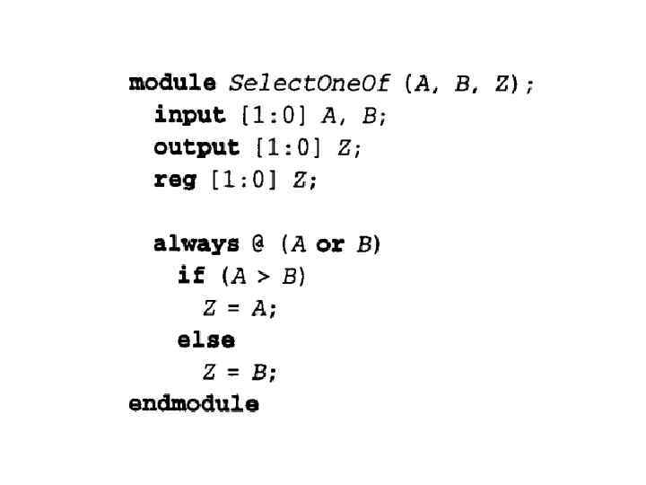
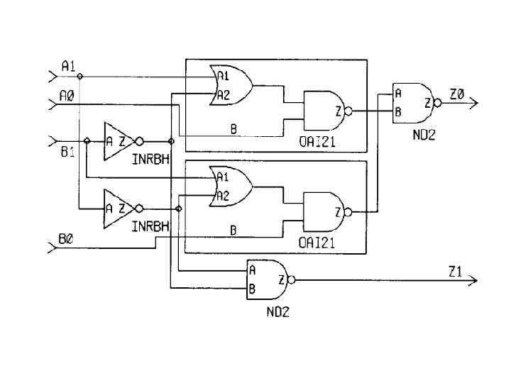
 <statements> always @(a or b") Процедурные блоки 1 2 3 4 5 always @(
Процедурные блоки 1 2 3 4 5 always @(
![reg [3: 0] c; always @(a or b or d) begin if (d) begin](https://present5.com/presentation/3/26829759_438461642.pdf-img/26829759_438461642.pdf-30.jpg "reg [3: 0] c; always @(a or b or d) begin if (d) begin") reg [3: 0] c; always @(a or b or d) begin if (d) begin c = a & b; end else begin c = a + b; end case (selector) option 1:
reg [3: 0] c; always @(a or b or d) begin if (d) begin c = a & b; end else begin c = a + b; end case (selector) option 1:
![wire [1: 0] option; wire [7: 0] a, b, c, d; reg [7: 0]](https://present5.com/presentation/3/26829759_438461642.pdf-img/26829759_438461642.pdf-31.jpg "wire [1: 0] option; wire [7: 0] a, b, c, d; reg [7: 0]") wire [1: 0] option; wire [7: 0] a, b, c, d; reg [7: 0] e; always @(a or b or c or d or option) begin case (option) 0: e = a; 1: e = b; 2: e = c; 3: e = d; endcase end
wire [1: 0] option; wire [7: 0] a, b, c, d; reg [7: 0] e; always @(a or b or c or d or option) begin case (option) 0: e = a; 1: e = b; 2: e = c; 3: e = d; endcase end
 Синхронная логика
![module DFF 8 (clock, data, q); input clock; input [7: 0] data; output [7:](https://present5.com/presentation/3/26829759_438461642.pdf-img/26829759_438461642.pdf-33.jpg "module DFF 8 (clock, data, q); input clock; input [7: 0] data; output [7:") module DFF 8 (clock, data, q); input clock; input [7: 0] data; output [7: 0] q; reg [7: 0] q; always @(posedge clock) begin q <= data; endmodule
module DFF 8 (clock, data, q); input clock; input [7: 0] data; output [7: 0] q; reg [7: 0] q; always @(posedge clock) begin q <= data; endmodule
![module DFFSR (reset, clock, data, q); input reset; input clock; input [7: 0] data;](https://present5.com/presentation/3/26829759_438461642.pdf-img/26829759_438461642.pdf-34.jpg "module DFFSR (reset, clock, data, q); input reset; input clock; input [7: 0] data;") module DFFSR (reset, clock, data, q); input reset; input clock; input [7: 0] data; output [7: 0] q; reg [7: 0] q; always @(posedge clock) begin if (reset) begin q <= 0; end else begin q <= data; end endmodule
module DFFSR (reset, clock, data, q); input reset; input clock; input [7: 0] data; output [7: 0] q; reg [7: 0] q; always @(posedge clock) begin if (reset) begin q <= 0; end else begin q <= data; end endmodule
![module DFFAR (reset, clock, data, q); input reset; input clock; input [7: 0] data;](https://present5.com/presentation/3/26829759_438461642.pdf-img/26829759_438461642.pdf-35.jpg "module DFFAR (reset, clock, data, q); input reset; input clock; input [7: 0] data;") module DFFAR (reset, clock, data, q); input reset; input clock; input [7: 0] data; output [7: 0] q; reg [7: 0] q; always @(posedge clock or posedge reset) begin if (reset) begin q <= 0; end else begin q <= data; end endmodule
module DFFAR (reset, clock, data, q); input reset; input clock; input [7: 0] data; output [7: 0] q; reg [7: 0] q; always @(posedge clock or posedge reset) begin if (reset) begin q <= 0; end else begin q <= data; end endmodule