47191d337f4def785c95fa18d4a374f1.ppt
- Количество слайдов: 25
 Power Pulsing using Saltro 16 and future power pulsing possibilities with the GDSP. The Present The Saltro 16 – overview Power Pulsing with the SAltro 16 Ideas for the Future Industrial Trends in Microelectronics Projections and ideas for the future – The GDSP Power Pulsing possibilities P. Aspell M. De Gaspari CERN Power Pulsing Workshop, May 2011
 Power Pulsing using Saltro 16 and future power pulsing possibilities with the GDSP. The Present The Saltro 16 – overview Power Pulsing with the SAltro 16 Ideas for the Future Industrial Trends in Microelectronics Projections and ideas for the future – The GDSP Power Pulsing possibilities P. Aspell M. De Gaspari CERN Power Pulsing Workshop, May 2011
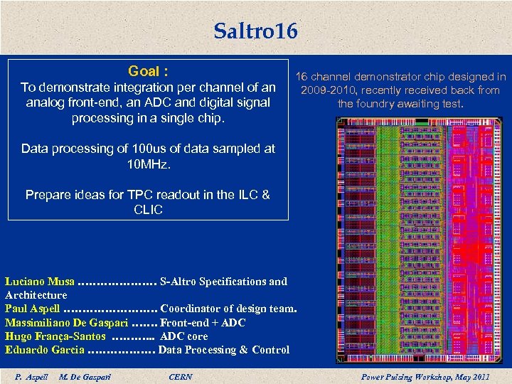 Saltro 16 Goal : To demonstrate integration per channel of an analog front-end, an ADC and digital signal processing in a single chip. 16 channel demonstrator chip designed in 2009 -2010, recently received back from the foundry awaiting test. Data processing of 100 us of data sampled at 10 MHz. Prepare ideas for TPC readout in the ILC & CLIC Luciano Musa ………………… S-Altro Specifications and Architecture Paul Aspell …………. Coordinator of design team. Massimiliano De Gaspari ……. Front-end + ADC Hugo França-Santos ………. . . ADC core Eduardo Garcia ……………… Data Processing & Control P. Aspell M. De Gaspari CERN Power Pulsing Workshop, May 2011
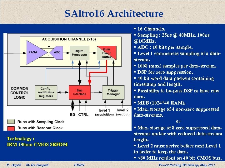 SAltro 16 Architecture § 16 Channels. § Sampling : 25 us @ 40 MHz, 100 us @10 MHz. § ADC : 10 bits per sample. § Level 1 commences sampling of a datastream. § 1008 (max) samples per data-stream. § DSP for zero suppression. § 40 bit word data packets containing timestamp and length. § Possibility to by-pass DSP to have raw data. § MEB (1024*40 RAM). § Max. storage of 4 non-zero suppressed data-streams. or § Max. storage of 8 zero suppressed datastreams and/or with reduced data-stream length. § Level 2 must arrive before next Level 1 in order to keep the data. § <80 MHz readout on 40 bit CMOS bus. Technology : IBM 130 nm CMOS 8 RFDM P. Aspell M. De Gaspari CERN Power Pulsing Workshop, May 2011
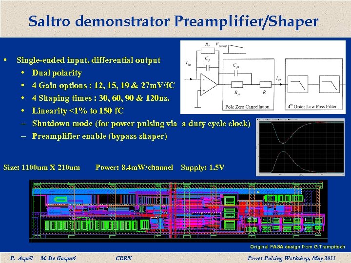 Saltro demonstrator Preamplifier/Shaper • Single-ended input, differential output • Dual polarity • 4 Gain options : 12, 15, 19 & 27 m. V/f. C • 4 Shaping times : 30, 60, 90 & 120 ns. • Linearity <1% to 150 f. C – Shutdown mode (for power pulsing via a duty cycle clock) – Preamplifier enable (bypass shaper) Size: 1100 um X 210 um Power: 8. 4 m. W/channel Supply: 1. 5 V Original PASA design from G. Trampitsch P. Aspell M. De Gaspari CERN Power Pulsing Workshop, May 2011
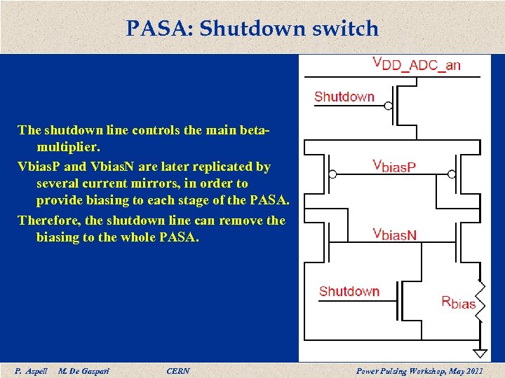 PASA: Shutdown switch The shutdown line controls the main betamultiplier. Vbias. P and Vbias. N are later replicated by several current mirrors, in order to provide biasing to each stage of the PASA. Therefore, the shutdown line can remove the biasing to the whole PASA. P. Aspell M. De Gaspari CERN Power Pulsing Workshop, May 2011
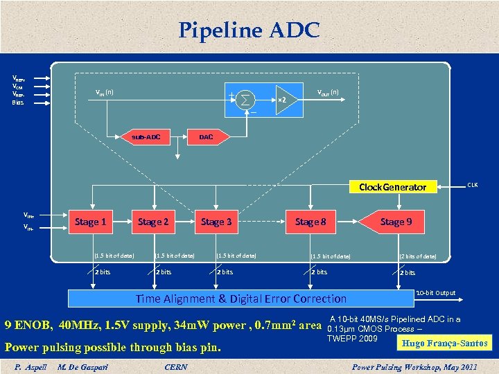 Pipeline ADC VREF+ VCM VREFBias VIN (n) × 2 VOUT (n) DAC sub-ADC Clock. Generator VIN+ VIN- Stage 1 Stage 2 Stage 3 Stage 8 Stage 9 (1. 5 bit of data) (2 bits of data) 2 bits 2 bits Time Alignment & Digital Error Correction 9 ENOB, 40 MHz, 1. 5 V supply, 34 m. W power , 0. 7 mm 2 area Power pulsing possible through bias pin. P. Aspell CLK M. De Gaspari CERN 10 -bit Output A 10 -bit 40 MS/s Pipelined ADC in a 0. 13μm CMOS Process – TWEPP 2009 Hugo França-Santos Power Pulsing Workshop, May 2011
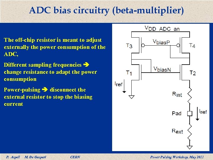 ADC bias circuitry (beta-multiplier) The off-chip resistor is meant to adjust externally the power consumption of the ADC, Different sampling frequencies change resistance to adapt the power consumption Power-pulsing disconnect the external resistor to stop the biasing current P. Aspell M. De Gaspari CERN Power Pulsing Workshop, May 2011
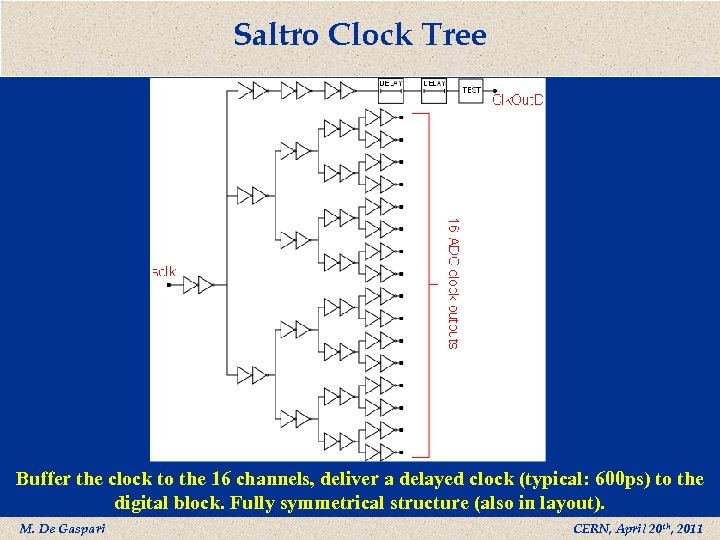 Saltro Clock Tree Buffer the clock to the 16 channels, deliver a delayed clock (typical: 600 ps) to the digital block. Fully symmetrical structure (also in layout). M. Aspell M. De Gaspari P. De Gaspari CERN, April 20 2011 Power Pulsing Workshop, May th, 2011
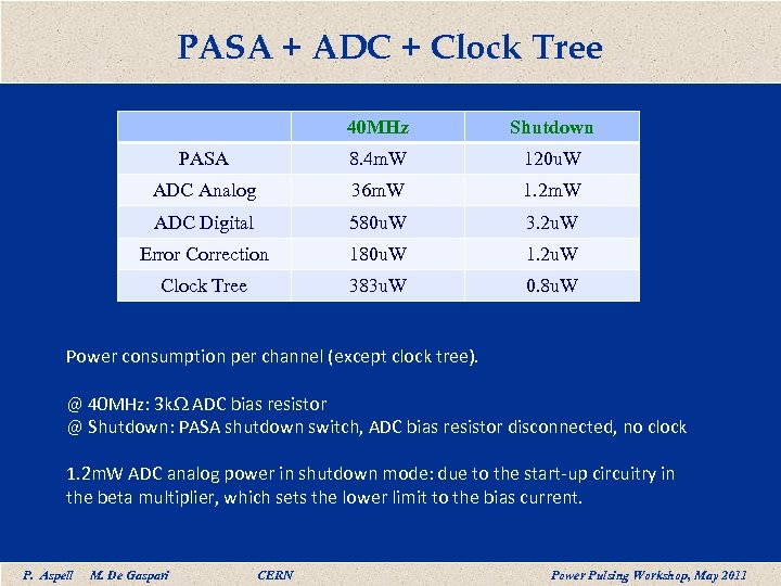 PASA + ADC + Clock Tree 40 MHz Shutdown PASA 8. 4 m. W 120 u. W ADC Analog 36 m. W 1. 2 m. W ADC Digital 580 u. W 3. 2 u. W Error Correction 180 u. W 1. 2 u. W Clock Tree 383 u. W 0. 8 u. W Power consumption per channel (except clock tree). @ 40 MHz: 3 k. W ADC bias resistor @ Shutdown: PASA shutdown switch, ADC bias resistor disconnected, no clock 1. 2 m. W ADC analog power in shutdown mode: due to the start-up circuitry in the beta multiplier, which sets the lower limit to the bias current. P. Aspell M. De Gaspari CERN Power Pulsing Workshop, May 2011
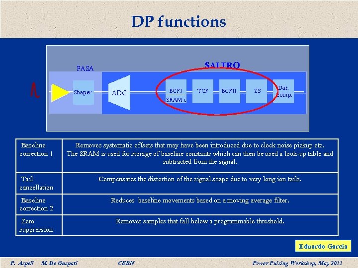 DP functions SALTRO PASA Shaper ADC BCFI SRAM 1 TCF BCFII ZS Dat. comp. Baseline correction 1 Removes systematic offsets that may have been introduced due to clock noise pickup etc. The SRAM is used for storage of baseline constants which can then be used a look-up table and subtracted from the signal. Tail cancellation Compensates the distortion of the signal shape due to very long ion tails. Baseline correction 2 Reduces baseline movements based on a moving average filter. Zero suppression Removes samples that fall below a programmable threshold. Eduardo Garcia P. Aspell M. De Gaspari CERN Power Pulsing Workshop, May 2011
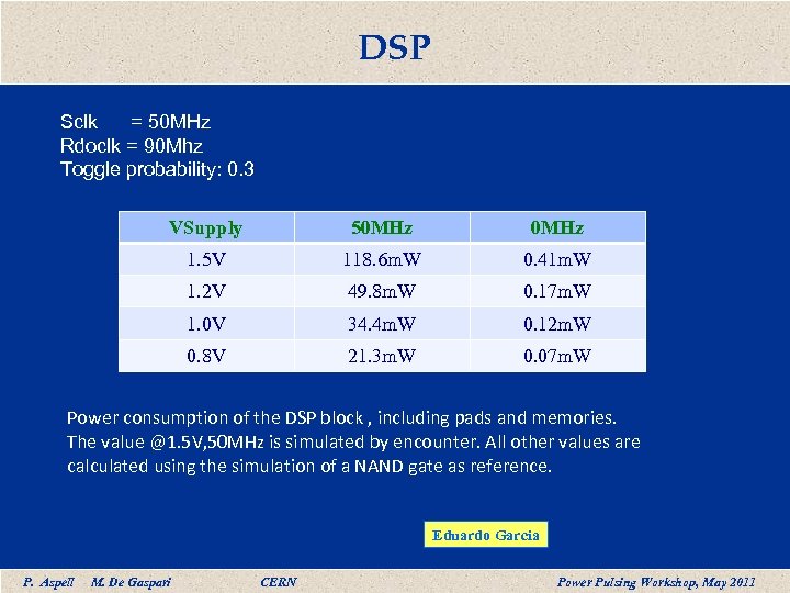 DSP Sclk = 50 MHz Rdoclk = 90 Mhz Toggle probability: 0. 3 VSupply 50 MHz 1. 5 V 118. 6 m. W 0. 41 m. W 1. 2 V 49. 8 m. W 0. 17 m. W 1. 0 V 34. 4 m. W 0. 12 m. W 0. 8 V 21. 3 m. W 0. 07 m. W Power consumption of the DSP block , including pads and memories. The value @1. 5 V, 50 MHz is simulated by encounter. All other values are calculated using the simulation of a NAND gate as reference. Eduardo Garcia P. Aspell M. De Gaspari CERN Power Pulsing Workshop, May 2011
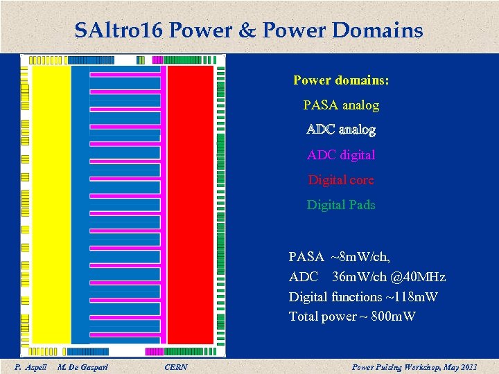 SAltro 16 Power & Power Domains Power domains: PASA analog ADC digital Digital core Digital Pads PASA ~8 m. W/ch, ADC 36 m. W/ch @40 MHz Digital functions ~118 m. W Total power ~ 800 m. W P. Aspell M. De Gaspari CERN Power Pulsing Workshop, May 2011
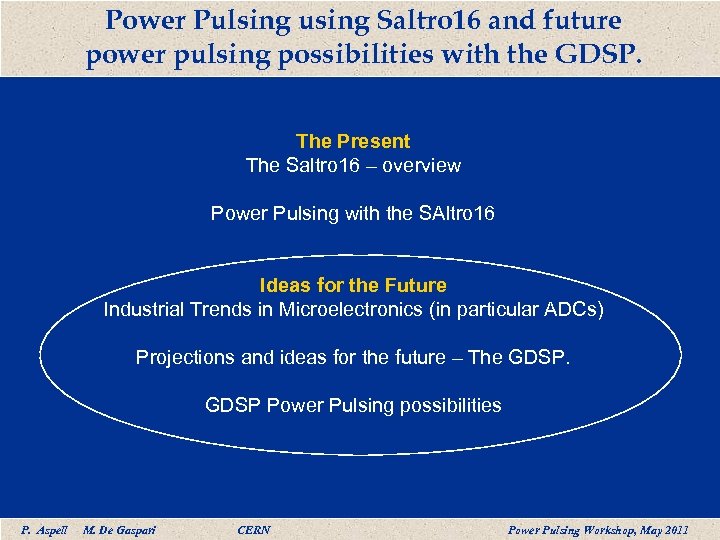 Power Pulsing using Saltro 16 and future power pulsing possibilities with the GDSP. The Present The Saltro 16 – overview Power Pulsing with the SAltro 16 Ideas for the Future Industrial Trends in Microelectronics (in particular ADCs) Projections and ideas for the future – The GDSP Power Pulsing possibilities P. Aspell M. De Gaspari CERN Power Pulsing Workshop, May 2011
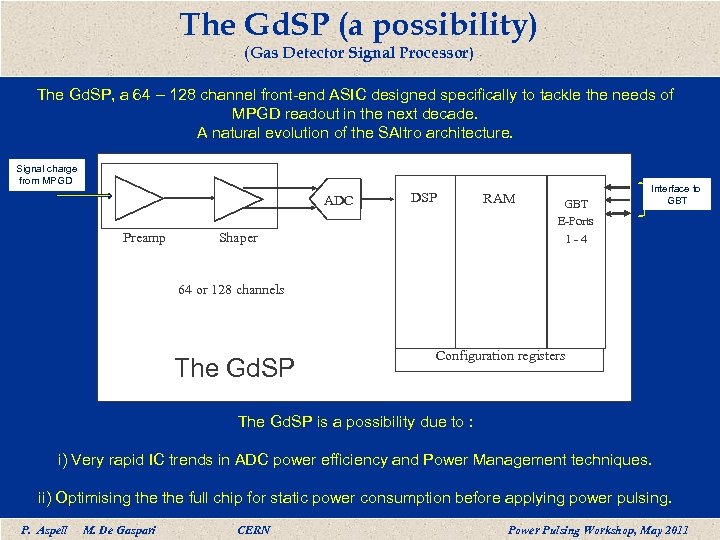 The Gd. SP (a possibility) (Gas Detector Signal Processor) The Gd. SP, a 64 – 128 channel front-end ASIC designed specifically to tackle the needs of MPGD readout in the next decade. A natural evolution of the SAltro architecture. Signal charge from MPGD ADC Preamp DSP Shaper RAM GBT E-Ports 1 -4 Interface to GBT 64 or 128 channels The Gd. SP Configuration registers The Gd. SP is a possibility due to : i) Very rapid IC trends in ADC power efficiency and Power Management techniques. ii) Optimising the full chip for static power consumption before applying power pulsing. P. Aspell M. De Gaspari CERN Power Pulsing Workshop, May 2011
 ADC Trends Source : A 550 u. W 10 b 40 MS/s SAR ADC with Multistep Addition-only Digital Error Correction, Sang-Hyun Cho et al. CICC 2010 (FOM = 42 f. J/conversion) designed in 0. 13 um CMOS P. Aspell M. De Gaspari CERN Power Pulsing Workshop, May 2011
 ADC Trends Source : A 550 u. W 10 b 40 MS/s SAR ADC with Multistep Addition-only Digital Error Correction, Sang-Hyun Cho et al. CICC 2010 (FOM = 42 f. J/conversion) designed in 0. 13 um CMOS P. Aspell M. De Gaspari CERN Power Pulsing Workshop, May 2011
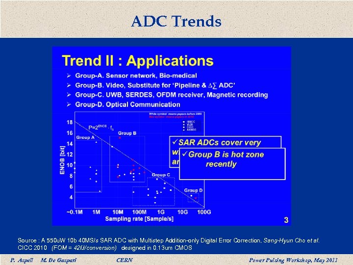
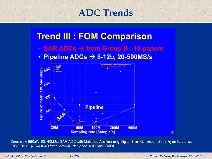
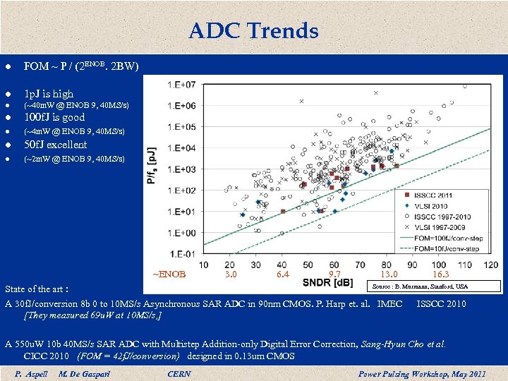 ADC Trends l FOM ~ P / (2 ENOB. 2 BW) l 1 p. J is high l (~40 m. W @ ENOB 9, 40 MS/s) l 100 f. J is good l (~4 m. W @ ENOB 9, 40 MS/s) l 50 f. J excellent l (~2 m. W @ ENOB 9, 40 MS/s) ~ENOB 3. 0 6. 4 9. 7 13. 0 16. 3 Source : B. Murmann, Stanford, USA State of the art : A 30 f. J/conversion 8 b 0 to 10 MS/s Asynchronous SAR ADC in 90 nm CMOS. P. Harp et. al. IMEC ISSCC 2010 [They measured 69 u. W at 10 MS/s, ] A 550 u. W 10 b 40 MS/s SAR ADC with Multistep Addition-only Digital Error Correction, Sang-Hyun Cho et al. CICC 2010 (FOM = 42 f. J/conversion) designed in 0. 13 um CMOS P. Aspell M. De Gaspari CERN Power Pulsing Workshop, May 2011
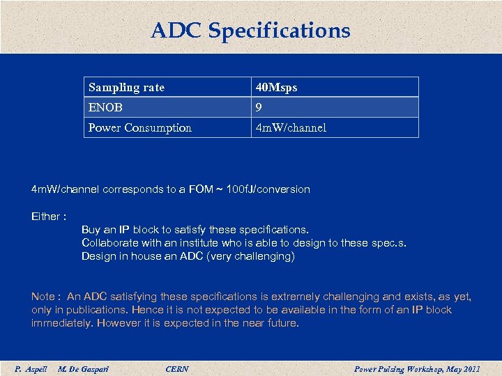 ADC Specifications Sampling rate 40 Msps ENOB 9 Power Consumption 4 m. W/channel corresponds to a FOM ~ 100 f. J/conversion Either : Buy an IP block to satisfy these specifications. Collaborate with an institute who is able to design to these spec. s. Design in house an ADC (very challenging) Note : An ADC satisfying these specifications is extremely challenging and exists, as yet, only in publications. Hence it is not expected to be available in the form of an IP block immediately. However it is expected in the near future. P. Aspell M. De Gaspari CERN Power Pulsing Workshop, May 2011
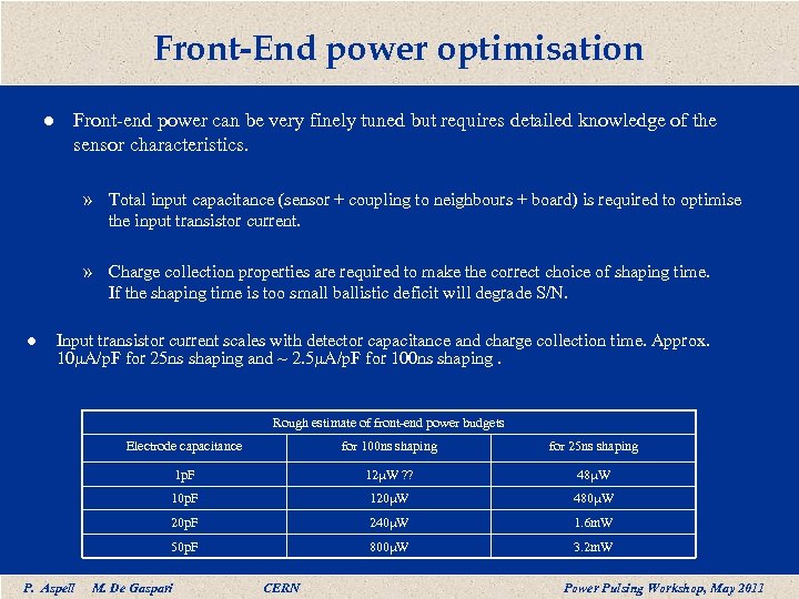 Front-End power optimisation l Front-end power can be very finely tuned but requires detailed knowledge of the sensor characteristics. » Total input capacitance (sensor + coupling to neighbours + board) is required to optimise the input transistor current. » Charge collection properties are required to make the correct choice of shaping time. If the shaping time is too small ballistic deficit will degrade S/N. l Input transistor current scales with detector capacitance and charge collection time. Approx. 10 m. A/p. F for 25 ns shaping and ~ 2. 5 m. A/p. F for 100 ns shaping. Rough estimate of front-end power budgets Electrode capacitance for 25 ns shaping 1 p. F 12 m. W ? ? 48 m. W 10 p. F 120 m. W 480 m. W 20 p. F 240 m. W 1. 6 m. W 50 p. F P. Aspell for 100 ns shaping 800 m. W 3. 2 m. W M. De Gaspari CERN Power Pulsing Workshop, May 2011
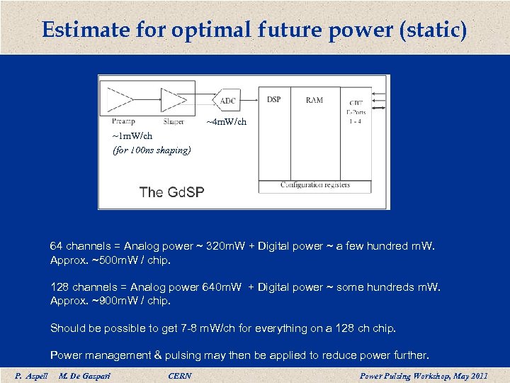 Estimate for optimal future power (static) ~4 m. W/ch ~1 m. W/ch (for 100 ns shaping) 64 channels = Analog power ~ 320 m. W + Digital power ~ a few hundred m. W. Approx. ~500 m. W / chip. 128 channels = Analog power 640 m. W + Digital power ~ some hundreds m. W. Approx. ~900 m. W / chip. Should be possible to get 7 -8 m. W/ch for everything on a 128 ch chip. Power management & pulsing may then be applied to reduce power further. P. Aspell M. De Gaspari CERN Power Pulsing Workshop, May 2011
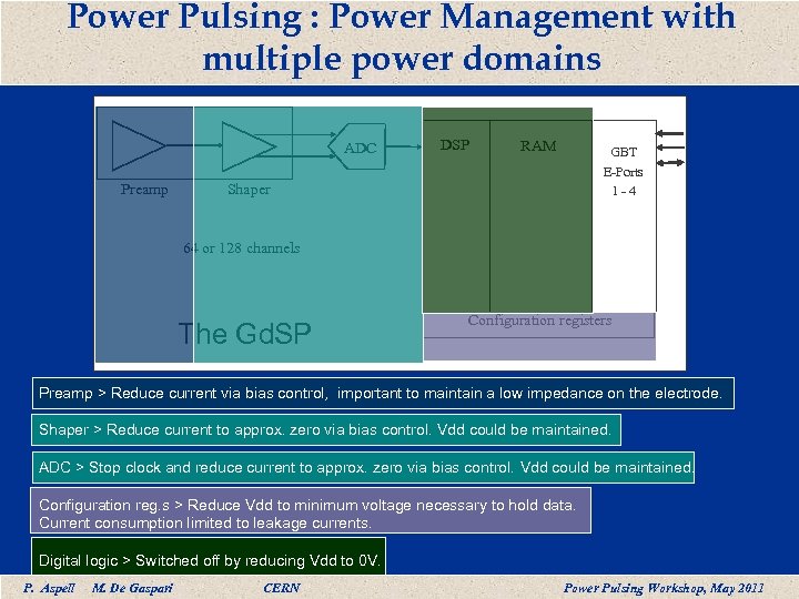 Power Pulsing : Power Management with multiple power domains ADC Preamp DSP RAM GBT E-Ports 1 -4 Shaper 64 or 128 channels The Gd. SP Configuration registers Preamp > Reduce current via bias control, important to maintain a low impedance on the electrode. Shaper > Reduce current to approx. zero via bias control. Vdd could be maintained. ADC > Stop clock and reduce current to approx. zero via bias control. Vdd could be maintained. Configuration reg. s > Reduce Vdd to minimum voltage necessary to hold data. Current consumption limited to leakage currents. Digital logic > Switched off by reducing Vdd to 0 V. P. Aspell M. De Gaspari CERN Power Pulsing Workshop, May 2011
 Power Pulsing Phases “Sampling”, “Read” and “Sleep” phases controlled by fast synchronous commands through the E-port. ADC Preamp DSP RAM Shaper GBT E-Ports 1 -4 64 or 128 channels The Gd. SP Configuration registers “Sampling” Phase = All modules “Up”. “Non Sampling” Phase = Preamp, Shaper and ADC “Down”, “Read” Phase = Preamp, Shaper and ADC “Down”, DSP RAM Configuration Reg. s and E-ports “Up” “Sleep” Phase = Preamp, Shaper, ADC, DSP, RAM “Down”, Configuration Registers and E-port “Up”. “Sampling” “Non Sampling” “Read” P. Aspell M. De Gaspari “Sleep” CERN Power Pulsing Workshop, May 2011
 Summary The SAltro 16 demonstrator chip exists and is awaiting test. . l » Comprises 16 channels of Front-end + ADC + DSP on the same chip. » Chip return back from foundry for beginning of 2011. » Many things can be studied using the SAltro demonstrator : – Internal power pulsing on front-end and ADC via clock and bias control. – The power consumption of the present 16 channel chip is about the same absolute value as future chips with more channels. This makes the demonstrator useful for groups studying external power pulsing. – GEM properties : capacitance, charge collection time, optimal shaping, channel to channel coupling etc. l The future looks favourably on the SAltro architecture, see GDSP. » The industrial trend is with us continually looking for ways to reduce power. » The ADC remains the critical element w. r. t. power, however state of the art ADCs are becoming more and more power efficient. » Power management within a chip is now common place in modern industrial chips and could be a useful tool for power pulsing. P. Aspell M. De Gaspari CERN Power Pulsing Workshop, May 2011
 Summary The SAltro 16 demonstrator chip exists and is awaiting test. . l » Comprises 16 channels of Front-end + ADC + DSP on the same chip. » Chip return back from foundry for beginning of 2011. » Many things can be studied using the SAltro demonstrator : – Internal power pulsing on front-end and ADC via clock and bias control. – The power consumption of the present 16 channel chip is about the same absolute value as future chips with more channels. This makes the demonstrator useful for groups studying external power pulsing. – GEM properties : capacitance, charge collection time, optimal shaping, channel to channel coupling etc. l The future looks favourably on the SAltro architecture, see GDSP. » The industrial trend is with us continually looking for ways to reduce power. » The ADC remains the critical element w. r. t. power, however state of the art ADCs are becoming more and more power efficient. » Power management within a chip is now common place in modern industrial chips and could be a useful tool for power pulsing. Both the SAltro 16 and the GDSP will be presented in more detail as 2 separate talks in the Saltro meeting this afternoon. P. Aspell M. De Gaspari CERN Power Pulsing Workshop, May 2011


